INSTRUCTION
MANUAL
REGULATED
POWER
SUPPLI
"
ES
MODEL LM
A PACKAGEINSTRUCTION MANUAL
FOR
REGULATED POWER SUPPLIES
MODEL LM
A PACKAGE
THIS MANUAL APPLIES TO UNITS
BEARING SERIAL NO. PREFIXES A-C
This manual provides instructions intended for
the operation of Lambda power supplies, and is
not to be reproduced without the written consent
of Lambda Electronics Corp.
LAMBDA ELECTRONICS CORP.
MELVILLE, L.1., N. Y.
MAIN PLANT TELEPHONE: 516 MYrtle 4-4200
SECTION
SPECIFICATIONS AND FEATURES Mounting
Accessories Model Options THEORY OF OPERATION
General
Functional Description OPERATING INSTRUCTIONS
Basic Mode of Operation Mounting
Connections for Operation MAINTENANCE
General
Trouble Analysis
TAB LE OF CONTENTS
Checking Transistors and Capacitors
SERVICE
Printed Circuit Board Maintenance Techniques Trouble Chart
Performance Check
Adjustment of Calibration Control R17
PARTS ORDERING
PARTS LIST
~
1
2
2 3 4 4 4 5 5 5 5
7 7 7 7 7 8 9
9
10 10
SPECIFICATIONS AND FEATURES
The following specifications apply for all Lambda A package LM power supplies. Speci-fication exceptions noted here relate to models incorporating model option "Y" and/or "T". Per-formance specifications do not change for models with suffix "R", e. g., LM-251R unless the models also include "model options "Y" and/or "T" e. g., LM-251YR; for these models the appro-priate specification exceptions also apply.
NOTE: Specifications in italics apply only for Lambda models with a "Y" suffix, e. g., LM-251Y. AC INPUT specification with an asterisk*, applies only for Lambda models with a "T" or "V" suffix, e. g., LM-251YT.
DC OUTPUT--Voltage regulated for line and load
Voltage Range .••. For voltage range see table I of pertinent model group.
Multi-Current Ratings .... Current ratings specified for each maximum ambient temper-ature apply over entire output voltage range, with input frequency 55-65 cps. For input frequencies 45-55 at 105-132 VAC, 200-250 VAC or 205-265 VAC, derate maxi-mum current ratings 10% at all ambient temperatures.
For input frequencies 360-440 cps, at 105-132 VAC, 200-250 VAC or 205-265 VAC, derate maximum current ratings 10% at all ambient temperatures.
Consult factory for current ratings on models LM-267, LM-268 with input frequencies 360-440 cps.
For maximum current ratings at each ambient temperature see table I of pertinent model group.
REGULATED VOLTAGE OUTPUT
Regulation (line) . . . Less than 0.05 percent plus 4.0 millivolts for input variations from 105-132 or 132-105 volts AC
· .. Less than O. 01 percent plus 1.0 millivolt for input variations from 105-132 or 132-105 volts AC
Regulation (load) ... Less than 0.03 percent plus 3.0 millivolts for load variations from
o
to full load or full load to 0· .. Less than O. 02 percent plus 2. 0 millivolts for load variations from
o
to full load or full load to 0Remote Programming
External Resistor ..• Nominal 200 ohms/volt output
Programming Voltage ..• One-to-one voltage change
Ripple and Noise ... One millivolt rms; 3 millivolts peak-to-peak with 60 cps input · .. O. 5 millivolt rms; 1.5 millivolts peak-to-peak with 60 cps input
· .• 1. 0 millivolt rms; 3 millivolts peak-to-peak with 400 cps input Temperature Coefficient ... Change in output voltage less than 0.03%/0 C
.•. Change in output voltage less than O. 01%/°C
AC INPUT--105-132 volts AC at 45-440 cps; for wattage + rating see table I of pertinent model group.
+ With output loaded to full 400C rating and input voltage 132 volts at 55-65 cps.
* ...
200-250 volts AC at 45-440 cps (nTn option)* ...
205-265 volts AC at 45-440 cps ("V" option)INPUT FUSE--When fusing of input power line is planned, use a 1. 25 ampere type 3AG "SLO-BLO" fuse. Overload of the supply does not cause fuse failure.
OVERLOAD PROTECTION
Thermal. .• On all units with thermostats, the thermostat resets automatically when over-temperature condition is eliminated
Electrical. •• Within rated voltage range, an automatic electronic current-limiting circuit limits output current to approximately 110 percent of 40°C rated current for protection of load and power supply.
OVERSHOOT--No overshoot of output voltage under conditions of power turn-on, power turn-off, or power failure.
INPUT AND OUTPUT CONNECTIONS--Heavy duty terminal block on rear of chassis
OPERATING AMBIENT TEMPERATURE RANGE AND DUTY CYCLE--Continuous duty from _20°C to 710 C ambient with corresponding load current ratings for all modes of operation, and all mounting positions.
STORAGE TEMPERATURE-- -550 C to +85°C
CONTROLS
DC output control. .. Voltage adjust control permits adjustment of DC output voltage via access hole located in nameplate.
REMOTE SENSING--Provision is made for remote sensing to eliminate effect of power output lead resistance on DC regulation.
PHYSICAL DATA
Size ••••••••••••• 3-3/16" H x 3-3/4" W x 6-1/2" D
Weight.. • • •• • . .• 5lbs. net; 6 lbs. shipping wt.
Finish •••••••••.• Grey, FED STD 595 No. 26081
MOUNTING--Three surfaces, each with tapped mounting holes, can be utilized for mounting this unit. Refer to figure 9 for mounting details.
ACCESSORIES
Rack Adapters ..• Rack adapters LRA-4 and LRA-6, used for ruggedized mounting, with or without chassis slides, are available, as well as rack adapters LRA-3 and LRA-5 which are used for simple rack installations where chassis slides are not required.
Metered and Non-Metered Panels .•. Metered panels MP-3, MP-5 and Non-Metered panets P-3, P-5 are available for use with the Lambda rack adapters.
BLANK PANELS
Rack Full Metered/Non
Adapter 1/2 Rack 1/4 Rack Rack Metered Panel
LRA 3 LBP-20 LBP-10 LBP-40 MP-5, P-5
LRA 6 LBP-20 LBP-10 LBP-40 MP-5, P-5
LRA 4 LBP-50 LBP-60 LBP-30 MP-3, P-3
LRA 5 LBP-50 LBP-60 LBP-30 MP-3, P-3
Overvoltage Protector ... Externally mounted, Overvoltage Protectors LMOV -1, LMOV-2 and LMOV -3 are available for use- with Lambda LM Power supplies.
MODEL OPTIONS
IM-LMA
Suffix "T" Input Option •.• Standard LM power supplies are available for operation with 200-250 volt, 45-440 cps input.
Suffix "Y" High Performance Option ... All Lambda LM power supplies are available with high performance specifications. See italicized entries under SPECIFICATIONS AND
FEATURES.
Suffix "R" Fungus Proofing Option .•. Standard LM power supplies can be obtained with fungus proofing treatment with MIL V 173 varnish for all fungi nutrient components. Suffix "V" Input Option ... Standard LM power supplies are available for operation with
205-265 volt, 45-440 cps input.
THEORY OF OPERATI ON
GENERAL
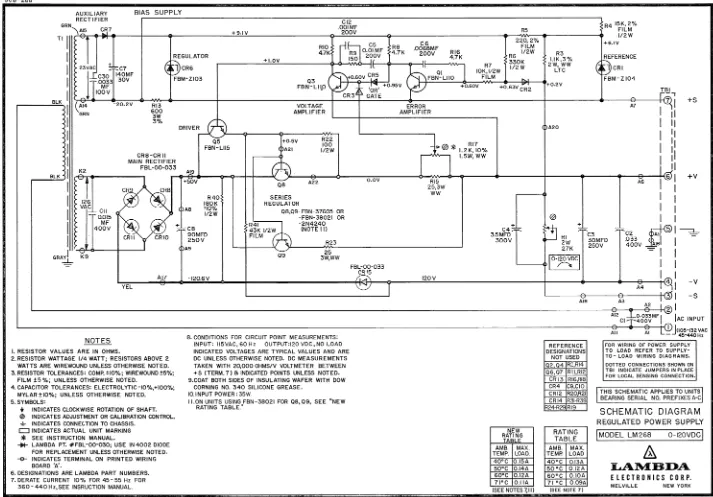
The Lambda power supply circuitry consists of an AC input circuit and transformer; a bias supply consisting of an auxiliary rectifier, filter, and a zener diode regulator; and a main regulator circuit consisting of the main rectifier and filter, a series regulator, emitter follower driver, an error amplifier, a voltage amplifier, an "OR" gate, and an output voltage sensing circuit.
The circuit arrangement is shown in block diagram form in figure 7. The circuitry is discussed with reference to the block diagram and the schematic diagram.
FUNCTIONAL DESCRIPTION
Single phase input power is applied to transformer T1 through the input circuit containing thermostat S1 *, which protects the supply against overheating.
The main rectifier, a full-wave rectifier (or half-wave rectifier, as applicable), provides the power which is filtered by capacitor C8 and then regulated via a series regulator and delivered to the output. Bias supply, half-wave, auxiliary rectifier CR7, provides voltage filtered by capa-citor C7 and regulated by zener diode CR6 for voltage amplifier Q3 and error amplifier Q1. Zener diode CR1 and resistor R5, across the bias supply, provide a regulated temperature compensated reference voltage. Resistor R4 compensates for input voltage variations.
Operation of the voltage regulator circuit is determined by changes in the output voltage. A change in the output voltage is sensed by sensing divider R1, R3 which compares output voltage with the +S reference voltage. This provides an error voltage at junction of Rl and R3 which is amplified by error amplifier Ql, and is current amplified by emitter follower driver Q5. The ampli-fied signal from Q5 controls the voltage across series regulator Q8 (and, as applicable Q9), which functions as the active regulating element, restoring output voltage to the proper level.
Current limit circuit operation is determined by changes in the load. When load current increases above the rated current value, the voltage drop across current sensing resistor R14* (or R15, as applicable) increases, driving OR gate diode CR3 on, and OR gate diode CR5 toward cut-off. The resulting base current supplied to voltage amplifier Q3, drives Q3 toward turn-on. With Q3 conducting, the current to driver Q5 decreases, limiting the base current to series regu-lator Q8 (and, as applicable Q9), which results in an increase of voltage across the series regula-tor and a decrease of the output voltage, effectively limiting the output current to a safe value. The current limit value is determined by the factory setting of current limit potentiometer R17*,
When operating conditions reach short circuit, the output voltage value decreases to zero and the current decreases to a predetermined current limit value and remains unchanged.
*S1 not used on models LM-251, LM-257, LM-259, LM-263, LM-265 and R17 used as current 'sensing resistor on these models; S1 not used on model'.'! LM-20l, LM-203, LM-260, LM-205
OPERATI NG INSTRUCTIONS
BASIC MODE OF OPERATION
This power supply operates as a constant voltage source provided the load current does not exceed the rated value at 400C. For continuous operation, load current must not exceed the
rating for each ambient temperature. When load current exceeds 110% of 400 C rating, both voltage
and current decrease until voltage reaches zero and the current decreases to a predetermined value.
MOUNTING
When using this unit as a mounted component, a cutout must be provided to permit free-flow of air through the unit. See figure 9 for cutout sizes and specific mounting details.
CONNECTIONS FOR OPERATION
NOTE: Make all connections to the unit before applying AC input power.
Ground Connections. The Lambda power supply can be operated either with negative or positive output terminal grounded. Both positive and negative ground connections are shown in the diagrams for all suggested output connections illustrated in this manual.
Connection Terminals. Make all connections to the supply at the terminal block on the rear of the supply. Apply input power to terminals 1 and 2; always connect the ungrounded (hot) lead to terminal 1.
The supply positive terminal is brought out to terminal 6; the negative terminal to ter-mina14.
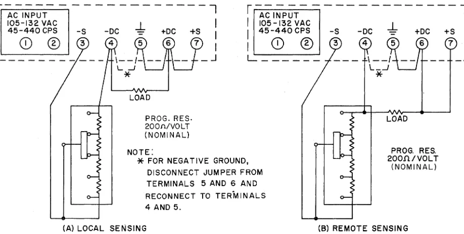
NOTE: When shipped from the factory, the supply is ready for use as a local-sensing constant voltage source. Jumpers are connected at the factory as shown in figure 3. Take care to remove the appropriate jumpers for load requirements that need different supply-load connections. Refer to the ap-propriate connection diagram.
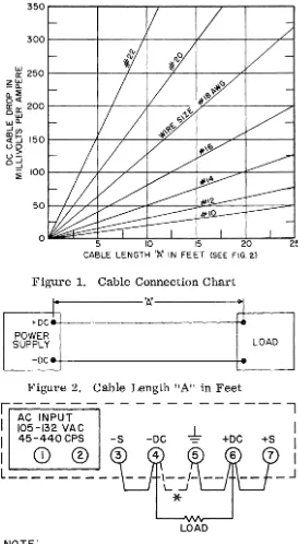
Supply-Load Connections. The regulation of the supply at the load may change when connecting leads of practical length are used. To minimize the effect of the output load leads, remote sensing is used. Refer to figure 1 to determine voltage drop for particular cable lenghts, wire size and current conditions. Lead lengths must be measured from supply terminals to load terminals as shown in figure 2.
Local-Sensing Connection, See Figure 3.
Remote-Sensing Connection, See Figure 4.
Programmed Voltage Connection Using External Resistor, See Figure 5. Discrete voltage steps can be programmed with a resistance voltage divider valued at nominal 200 ohms/volt output and a shorting-type switch. For continuous voltage variations, use a variable resistor with the same ohms/volt ratio in place of the voltage divider and shorting-type switch. Use low temperature co-efficient resistor(s) to assure most stable operation.
Programmed Voltage Connection Using Programming Voltage, See Figure 6. The power supply voltage output can be programmed with an externally connected programming power supply. The output voltage of the programmed supply will maintain a one-to-one ratio with the voltage of the programming supply.
The programming supply must have a reverse current capability of 6 mao minimum.
Alternatively, when supplies with less than 6 rna. reverse current capability are used, a resistor capable of drawing 6 rna. at the minimum programming voltage must be connected across the output terminals of the supply. This programming supply must be rated to handle all excess resistor current at the maximum programming voltage.
MA I NTENANCE
GENERAL
This section describes trouble analysis routine, calibration and test procedures that are useful for servicing the Lambda power supply. A trouble chart is provided as an aid for the troubleshooter. Refer to the section on SPECIFICATIONS AND FEATURES for the minimum per-formance standards.
TROUBLE ANALYSIS
Whenever trouble occurs, systematically check all fuses, primary power lines, external circuit elements, and external wiring for malfunction before trouble shooting the equipment. Failures and malfunctions often can be traced to simple causes such as improper jumpers and supply-load connections or fuse failure due to metal fatigue.
Use the electrical schematic diagram and block diagram, figure 7, as an aid to locating trouble causes. The schematic diagram contains various circuit voltages that are averages for normal no load operation. Measure these voltages using the conditions for measurement specified on the schematic diagram. Use measuring probes carefully to avoid causing short circuits and damaging circuit components.
CHECKING TRANSISTORS AND CAPACITORS
Check transistor with an in-circuit transistor checker. If no checker is available, transistors can be checked with an ohmmeter that has a highly limited current capability. Observe proper polarity for PNP or NPN to avoid error in measurement. The forward transistor resist-ance is low but never ZERO; backward resistresist-ance is always higher than the forward resistresist-ance. Do not assume trouble is eliminated when only one part is replaced. This is especially true when one transistor fails, causing other transistors to fail. Replacing only one transistor and turning power on, before checking for additional faulty components could damage the replaced component.
When soldering semi-conductor devices, hold the lead being soldered with a pair of pliers or a commercial heat sink device placed between the component and the solder joint.
NOTE: The leakage resistance obtained from a simple resistance check of a capacitor is not always an indication of a faulty capacitor. In all cases the capacitors are shunted with resistances, some of which have low values. Only a dead short is a true indication of a shorted capacitor.
PRINTED CIRCUIT BOARD MAINTENANCE TECHNIQUES
1. If foil is intact but not covered with solder it is a good contact. Do not attempt to cover with solder.
2. Voltage measurements can be made from either side of the board. Use a needle-point probe to penetrate to the wiring whenever a protective coating is used on the wiring. A brass probe can be soldered to an alligator clip adapted to measuring instrument. 3. Always use a heat sink when soldering transistors; a transistor pad with mounting feet
is an effective heat sink.
4. Broken or damaged printed wiring is usually the result of an imperfection, strain or careless soldering. To repair small breaks, tin a short piece of hook-up wire to bridge
the break, and holding the wire in place, flow solder along the length of wire so that it becomes part of the circuitry.
5. When unsoldering components from the board never pryor force loose the part; unsolder the component by using the wicking process described below:
(a) Select a 3/16 inch tinned copper braid for use as a wick; if braid is not available, select AWG No. 14 or No. 16 stranded wire with 1/2 inch insulation removed.
(b) Dip the wick in liquid rosin flux.
(c) Place the wick onto the soldered connection and apply soldering iron onto the wick.
(d) When sufficient amount of solder flows onto the wick, freeing the component, simul-taneously remove iron and wick.
TROUBLE CHART
The trouble chart is intended as a guide for locating trouble causes, and is used along with the schematic diagram.
The operating conditions assumed for the trouble chart are as follows:
(a) AC power of proper voltage and frequency is present at input terminals.
(b) Either positive or negative terminal is connected to chassis ground.
(c) The power supply is connected for constant voltage with local sensing. See schematic; dotted lines indicate jumpers connected for local sensing operation.
Symptom
1. No output volt-age
2. Unable to ad-just output voltage
TROUBLE CHART
Probable Cause
No power input, thermostat Sl open (as applicable)
Improper output terminal connec-tion
Faulty Q3, CR1, CR6
Remedy
Check power source, Sl, line cord and line cord plug; shut off unit, allow to cool and check ambient tempera-ture
Refer to appropriate connec-tion diagram, and check for correct connections
Check Q3, CR1, CR6 for short and replace as required
Damaged VOLTAGE ADJUST control Check Rl for shorts and/or open; replace as required
Supply operating as constant current source at current limit value
Symptom 3. Output voltage too high
4. Output voltage too low
5. High ripple and unregulated DC output·
6. High ripple
PERFORMANCE CHECK
TROUBLE CHART (Cont'd)
Probable Cause
Improper output terminal connec-tion
Faulty Ql, Rl, Q8 (and Q9, as applicable), Q5, or CRl
Load resistance improper for unit ratings
Faulty Q3, Rl4 or Rl5 or Rl7 (as applicable)
Load resistance improper for unit ratings
Improper ground
Remedy
Refer to appropriate connec-tion diagram, and check for correct connections
Check Rl for open; Q8 (Q9), Q5, Ql for short; CRl for open and replace as required.
Check load resistance value
Check Q3 for short, R14 or R15 or R17 for open, replace as required
Check load resistance value
Connect terminal 6 or termi-nal 4 to ground termitermi-nal 5
Check the ripple and regulation of the power supply using the test connection diagram shown in figure 8. Use suggested test equipment or equivalent to obtain accurate results. Refer to SPECIFICATIONS AND FEATURES for minimum performance standards.
Set the differential meter, DC VTVM (John Fluke Model 825A or equivalent) to the select-ed power supply operating voltage. Check the power supply load regulation accuracy while switch-ing from the full-load to no-load condition. Long load leads should be a twisted pair to minimize AC pick-up.
Use a Variac to vary the line voltage from 105-132 or 132-105 volts AC and check the power supply line regulation accuracy on the VTVM differential meter.
Use a VTVM Ballantine 320 or equivalent, to measure rms ripple voltage of the power supply DC output. Use oscilloscope to measure peak-to-peak ripple voltage of the power supply DC output.
ADJUSTMENT OF CALIBRATION CONTROL R17
Whenever Q3, Rl5 or Rl4 or Rl7 are replaced, and voltage and current indications do not re-flect maximum ratings, adjust R17 as follows:
NOTE: The following procedure requires that the power supply is removed from associated equipment, is on the bench at an ambient temperature of 25-300C, and is cold from not operating.
1. Remove AC power input to the supply.
2. Unsolder the wiper of R17 from resistor housing and turn to full CW position.
Adjustment of Calibration Control R17 (Cont'd)
3. Operate power supply for constant voltage with local sensing, connected as shown in Figure 3, with no external load.
4. Turn voltage adjust control until maximum non-derated output voltage is obtained.
5. Apply load so that output current is 130% of 400 C rating for the unit.
6. Using an oscilloscope, Tektronix 503 or equivalent, observe unit output voltage while adjusting R17 in a CCW direction. Adjust R17 until output ripple increases sharply and oscilloscope pattern changes.
7. Place a DC ammeter of appropriate scale across output terminals 4 and 6 of the supply. The meter indication shall be a maximum of 133% of 40°C rating for the unit.
8. After adjustment is completed, remove AC power input to the supply and solder wiper of R17 to resistor housing.
9. After soldering, check setting and repeat adjustment procedure if required.
SERVICE
When additional instructions are required or repair service is desired, contact the nearest office of the Lambda Electronics Corp. where trained personnel and complete facilities are ready to assist you.
Please include the power supply model and serial number together with complete details of the problem. On receipt of this information, Lambda will supply service data or advise shipping for factory repair service.
All repairs not covered by the warranty will be billed at cost and an estimate forwarded for approval before work is started.
PARTS ORDER I NG
Standard Components and special components used in Lambda power supply can be ob-tained from the factory. In case of emergency, critical spare parts are available through any Lambda office.
The following information must be included when ordering parts:
1. Model number and serial number of power supply and purchase date.
2. Lambda part number.
3. Description of part together with circuit designation.
PARTS LI ST
The electrical parts located on all LM-A package models are listed here. Parts common
to a group of LM-A models are listed first. Unique parts of individual models within the group
are listed separately, by model, immediately following the group common-parts listing. In
addition there are separate listings of parts for the metered panel (MP) option, the Y option,
the "T" option, "V" option, "R" option and the overvoltage protection (OV) option, as applicable
for all LM-A models.
ALL "A" PACKAGE MODELS EXCEPT LM-267, LM-268 ALL "A" PACKAGE MODELS EXCEPT LM-267, LM-268 (Cant)
COMMON PARTS COMMON PARTS (Cant)
CIRC. LAMBDA UNIT CIRC. LAMBDA UNIT
DESIG. DESCRIPTION NO. PRICE DESIG. DESCRIPTION NO. PRICE
C1 Cap., mylar, 0.033 mfd CGL-33-006 $ .27 Rll, Not asSigned $
±1O%, 400 vdc R12
C2 Cap., mylar, 0.22 mfd CGM-22-003 .33 R13* Res., ww, 600 ohms DFR-60-005 .89
±1O%, 100 vdc ±3%, 3w
C4 Cap., elect., 3.0 mfd CBN-30-015 1. 58 *This part not used on units with "Y" option -10 +75%, 100 vdc
C5 Cap., mylar, 0.01 mfd CGL-10-002 .36 UNlQUE PARTS
± 10%, 200 vdc
C7* Cap., elect., 140 mfd CBR-14-030 2.25 MODEL LM-201
-10 + 100%, 30 vdc
C3 Cap., elect., 400 mfd CBR-40-034 2.38
C12 Cap., mylar, 0.001 mfd CGK-10-004 .46
±10%, 200 vdc -10 + 100%, 30 vdc
CR1* Rectifier, zener diode FBM-Z104 4.35 C6 Cap., mylar, 0.001 mfd CGK-10-004 .21
CR2, Rectifier FBL-00-030 1. 40 ± 10%, 200 vdc
CR3 C8 Cap., elect., 1,700 mfd CBS-17-035 2.73
CR4 Not assigned -10 + 100%, 20 vdc
CR5 Same as CR2 C9, Cap., mylar, 0.018 mfd CGL-18-005 .24
CR6 Rectifier, zener diode FBM-Z103 4.87 C10 ±10%, 200 vdc
CR7 Same as CR2 Cll Not asSigned
Q1 Transistor, NPN FBN-LllO 3.25 CR8 Rectifier FBL-00-036 .60
Q2 Not asSigned CR9 Not asSigned
Q3 Same as Q1 CR10 Same as CR8
Q4 Not asSigned CRll Not assigned
Q6, Not assigned CR12 Rectifier FBL-00-030 1.40
Q7 Q5 Transistor, NPN FBN-L109 2.75
R2 Not assigned Q8 Transistor, NPN FBN-36603 3.25
R3 Res., ww, 1,100 ohms DFS-ll-061 .60 R1 Res., var., ww, 2,200 DNS-22-023 or 1. 75
±3%, 2w ohms ±5%, 5w DNS-22-053 2.50
R4* Res., film, 15,000 ohms DCT-15-013 .70 R14 Not assigned
±2%, 1/2w R15 Res., ww, 1. 5 ohms DFN-15-042 .60
R5 Res., film, 220 ohms DCR-22-005 .30 ±3%, 3w
±2%, 1/2w R16 Res., comp., 2,700 DCB-2721 .10
R6 Res., camp., 180,000 DCB-1841 .10 ohms ± 10%, 1/4w
ohms ± 10%, 1/4w R17 Res., var., ww, 1,200 DNS-12-026 1.25
R7 Res., film, 3, 900 ohms DCS-39-014 .25 ohms ±10%, 1-1/2w
±5%, 1/2w R18 Res., comp., 820 ohms DGB-82ll .08
R8 Res., camp., 4,700 DCB-4721 .10 ±10%, 1w
ohms ±10%, 1/4w R19 Res., camp., 1800 ohms DGB-1821 .08
R9 Res., camp., 150 ohms DCB-15ll .10 ±10%, 1w
±1O%, 1/4w R20, Not assigned
R10 Res., comp., 3,900 DCB-3921 .10 R21
ohms ±1O%, 1/4w R22 Res., camp., 100 ohms DEB-lOll .12
±10%, 1/2w
T1 Transformer ABA-201 16.00
UNIQUE PARTS (Cant) UNIQUE PARTS (Cant)
MODEL LM-202 MODEL ~ (Cant)
CIRC. LAMBDA UNIT CIRC. LAMBDA UNIT
DESIG. DESCRIPTION NO. PRICE DESIG. DESCRIPTION NO. PRICE
C3 Cap., elect., 400 mfd CBR-40-034 $ 2.38 C9, Cap., mylar, 0.018 mfd CGL-18-005
$ .24
-10 + 100%, 30 vdc CI0 ±10%, 200 vdc
C6 Cap., mylar, 0.001 mfd CGK-10-004 .21 Cll Not assigned
± 10%, 200 vdc CR8 Rectifier FBL-00-036 .60
C8 Cap., elect., 1,700 mfd CBS-17 -035 2.73 CR9 Not assigned
-10 + 100%, 20 vdc CRI0 Same as CR8
C9, Cap., mylar, 0.018 mfd CGL-18-005 .24 CRll Not assigned
C10 ±10%, 200 vdc CR12 Rectifier FBL-00-030 1.40
Cll Not assigned Q5 Transistor, NPN FBN-L109 2.75
CR8 Rectifier FBL-00-063 1.10 Q8 TranSistor, NPN FBN-36485 4.13
CR9 Not assigned R1 Res., var., WW, 4, 500 DNS-45-024 or 1. 75
CRI0 Same as CR8 ohms ±5%, 5w DNS-45-059 2.50
Q5 TransIstor, NPN FBN-L109 2.75 R14 Not assigned
Q8 Transistor, NPN FBN-36485 4.13 R15 Res., WW, 1. 5 ohms DFN-15-042 .60
R1 Res., var., ww, 2,200 DNS-22-023. or 1. 75 ±3%, 3w
ohms ±5%, 5w DNS-22-053 2.50 R16 Res., camp., 4,700 DCB-4721 .10
R14 Res., WW, 0.75 ohm DFM-75-044 .82 ohms ±10%, 1/4w
±5%, 5w R17 Res., var., WW, 1,200 DNS-12-026 1.25
R15 Not assigned ohms ±10%, 1-1/2w
R16 Res., camp., 2,700 DCB-2721 .10 R18 Not assigned
ohms ±10%, 1/4w R19 Res., camp., 3, 900 DGB-3921 .08
R17 Res., var., WW, 1,200 DNS-12-026 1. 25 ohms ±10%, 1w
ohms ±10%, 1-1/2w R20, Res., comp., 1, 800 DGB-1841 .08
R18 Res., film, 680 ohms DCR-68-009 1. 63 R21 ohms ±10%, 1w
±5%, 1/2w R22 Res., camp., 100 ohms DEB-lOll .12
R19 Not assigned ±10%, 1/2w
Thru T1 Transformer ABA-204 16.00
R21
R22 Res., camp., 100 ohms DEB-lOll .12 MODEL~
±1O%, 1/2w C3 Cap., elect., 70 mfd CBP-70-012 2.38
T1 Transformer ABA-202 16.00 -10 + 100%, 90 vdc
MODEL LM-203
C6 Cap., mylar, 0.001 mfd CGK-10-004 .21
C3 Cap., elect., 400 mfd CBR-40-034 2.38 ±10%, 200 vdc
-10 + 100%, 30 vdc C8 Cap., elect., 530 mfd CBR-53-035 2.75
C6 Cap., mylar, 0.001 mfd CGK-10-004 .21 -10 + 100%, 60 vdc
± 10%, 200 vdc C9, Cap., mylar, 0.018 mfd CGL-18-005 .24
C8 Cap., elect., 1, 000 mfd CBS-10-025 3.01 C10 ±10%, 200 vdc
-10 + 100%, 28 vdc Cll Not assigned
C9, Cap., mylar, 0.018 mfd CGL-18-005 .24 CR8 Rectifier FBL-00-036 .60
C10 ± 10%, 200 vdc CR9 Not assigned
Cll Not assigned CRlO Same as CR8
CR8 Rectifier FBL-00-036 .60 CRll Not assigned
CR9 Not assigned CR12 Rectifier FBL-00-030 1. 40
CR10 Same as CR8 Q5 Transistor, NPN FBN-L109 2.25
CRll Not assigned Q8 Transistor, NPN FBN-36605 5.00
CR12 Rectifier FBL-00-030 1. 40 R1 Res., var., WW, 9,000 DNS-90-025 or 2.00
Q5 TranSistor, NPN FBN-L109 2.75 ohms ±5%, 5w DNS-90-051 2.50
Q8 Transistor, NPN FBN-36603 3.25 R14 Not assigned
R1 Res., var., WW, 4,500 DNS-45-024 or 1. 75 R15 Res., WW, 6. 0 ohms DFN-60-054 .83
ohms ±5%, 5w DNS-45-059 2.50 ±3%, 3w
R14 Not asSigned R16 Not assigned
R15 Res., WW, 3.0 ohms DFN-30-023 .59 R17 Res., var., WW, 1,200 DNS-12-026 1.25
±3%, 3w ±10%, 1-1/2w
R16 Res., camp., 4,700 DCB-4721 .10 R18 Res., WW, 1,500 ohms DFS-15-045 .70
ohms ±10%, 1/4w ±3%, 3w
R17 Res., var., WW, 1, 200 DNS-12-026 1. 25 R19 Res., camp., 27,000 DEB-273l .12
ohms ±1O%, 1-1/2w ohms ±10%, 1/2w
R18 Res., camp., 1, 800 DGB-1821 .08 R20, Not assigned
ohms ±1O%, 1w R21
R19 Res., comp., 3,900 DGB-3921 .08 R22 Res., comp., 100 ohms DEB-lOll .12
ohms ±10%, 1w ±10%, 1/2w
R20, Not assigned T1 Transformer ABA-205 16.00
R21
R22 Res., camp., 100 ohms DEB-lOll .12 MODEL~
±10%, 1/2w C3 Cap., elect., 70 mfd CBP-70-012 2.38
T1 Transformer ABA-203 16.00 -10 + 100%, 90 vdc
MODEL LM-204 C6 Cap., mylar, 0.001 mfd CGK-1O-004 .21
C3 Cap., elect., 400 mfd CBR-40-034 2.38 ±lO%, 200 vdc
-10 + 100%, 30 vdc C8 Cap., elect., 530 mfd CBR-53-035 2.75
UNIQUE PARTS (Cont) UNIQUE PARTS (Cont)
MODEL LM-206 (Cont) MODEL ~ (Cont)
CIRC. LAMBDA UNIT CIRC. LAMBDA UNIT
DESIG. DESCRIPTION NO. PRICE DESIG. DESCRIPTION NO. PRICE
CR8 Rectifier FBL-00-036 $ .60 CRll Not assigned
CR9 Not assigned CR12 Rectifier FBL-00-030 $ 1. 40
CRI0 Same as CR8 Thru
CRll Not assigned CR15
CR2 Rectifier FBL-00-030 1. 40 Q5 Transistor, NPN FBN-L108 2.52
Q5 Transistor, NPN FBN-L108 2.52 Q8 Transistor, NPN FBN-35902 9.90
Q8 Transistor, NPN FBN-36487 5.63 R1 Res., var., WW, 13,000 DNT-13-008 or 2.48
Rl Res., var., ww, 9,000 DNS-90-025 or 2.00 ohms ±5%, 5w DNT-13-031 2.50
ohms ±5%, 5w DNS-90-051 2.50 R14 Not assigned
R14 Not assigned R15 Res., ww, 6.0 ohms DFN-60-054 .83
R15 Res., ww, 3.0 ohms DFN-30-023 .59 ±3%, 3w
±3%, 3w R16 Not assigned
R16 Not assigned R17 Res., var., WW, 1,200 DNS-12-026 1. 25
R17 Res., var., WW, 1,200 DNS-12-026 1. 25 ohms ±10%, 1-1/2w
ohms ±10%, 1-1/2w R18 Not assigned
R18 Not assigned R19 Res., comp., 47,000 DEB-4731 .12
R19 Res., comp., 27,000 DEB-2731 .12 ohms ±10%, 1/2w
ohms ±10%, 1/2w R20, Res., WW, 4,500 ohms DFS-45-044 .87
R20, Res., WW, 2,000 ohms DFS-20-032 .87 R21 ±3%, 3w
R21 ±3%, 3w R22 Res., comp., 100 ohms DEB-lOll .12
R22 Res., comp., 100 ohms DEB-lOll .12 ±10%, 1/2w
±1O%, 1/2w T1 Transformer ABA-208 20.50
T1 Transformer ABA-206 16.00
MODEL LM-251 MODEL LM-207
C3 Cap., elect., 400 mfd CBR-40-034 2.38
C3 Cap., elect., 70 mfd CBP-70-012 2.38 -10 + 100%, 30 vdc
-10 + 100%, 90 vdc C6 Cap., mylar, 0.0068 mfd CGK-68-001 .34
C6 Cap., mylar, 0.001 mfd CGK-10-004 .46 ±10%, 200 vdc
±10%, 200 vdc C8 Cap., elect., 1, 700 mfd CBS-17-035 2.73
C8 Cap., elect., 250 mfd CBR-25-024 1. 73 -10 + 100%, 20 vdc
-10 + 100%, 100 vdc C9 Cap., mylar, 0.018 mfd CGL-18-005 .24
C9, Cap., mylar, 0.015 mfd CGL-15-007 .31 ±10%, 200 vdc
CI0 ±10%, 400 vdc C10, Not assigned
Cll Not asSigned Cll
CR8 Rectifier FBL-00-033 1.65 CR8 Rectifier FBL-00-036 .60
CR9 Not asSigned Q5 TranSistor, NPN FBN-L109 2.75
CR10 Same as CR8 Q8 Transistor, NPN FBN-36486 2.75
CRll Not assigned R1 Res., var., WW, 2,200 DNS-22-023 or 1. 75
CR12 Rectifier FBL-00-030 1. 40 ohms ±5%, 5w DNS-22-053 2.50
Thru R14, Not assigned
CR15 R15
Q5 Transistor, NPN FBN-L108 2.52 R16 Res., comp., 2, 700 DCB-2721 .10
Q8 Transistor, NPN FBN-36606 5.00 ohms ±10%, 1/4w
R1 Res., var., ww, 13,000 DNT-13-008 or 2.48 R17 Res., var., WW, 10 ohms DNP-1O-004 .60
ohms ±5%, 5w DNT-13-031 2.50 ±10%, 3w
R14 Not asSigned R18 Res., film, 680 ohms DCR-68-009 1. 63
R15 Res., WW, 6.0 ohms DFN-60-054 .83 ±5%, 1/2w
±3%, 3w R19 Not assigned
R16 Not asSigned Thru
R17 Res., var., ww, 1,200 DNS-12-026 1. 25 R21
ohms ±1O%, 1-1/2w R22 Res., comp., 680 ohms DEB-68ll .12
R18 Res., ww, 4,500 ohms DFS-45-044 .87 ±10%, 1/2w
±3%, 3w Tl Transformer ABA-251 16.00
R19 Res., comp., 47,000 DEB-4731 .12
ohms ±10%, 1/2w MODEL LM-252
R20, Not asSigned
R21 C3 Cap., elect., 400 mfd CBR-40-034 2.38
R22 Res., comp., 100 ohms DEB-lOll .12 -10 + 100%, 30 vdc
±1O%, 1/2w C6 Cap., mylar, 0.0068 mfd CGK-68-001 .34
T1 Transformer ABA-207 16.00 ±10%, 200 vdc
C8 Cap., elect., 1, 700 mfd CBS-17 -035 2.73
MODEL LM-208 -10 + 100%, 20 vdc
C3 Cap., elect., 70 mfd CBP-70-012 2.38 C9, C10 Not assigned
-10 + 100%, 90 vdc Cll Cap., mylar, 0.018 mfd CGL-18-005 .24
C6 Cap., mylar, 0.001 mfd CGK-1O-004 .46 ±10%, 200 vdc
± 10%, 200 vdc CR8 Rectifier FBL-00-047 .88
C8 Cap., elect., 250 mfd CBR-25-024 1.73 Thru
-10 + 100%, 100 vdc CRll
C9, Cap., mylar, 0.015 mfd CGL-15-007 .31 Q5 TranSistor, NPN FBN-L109 2.75
C10 ± 10%, 400 vdc Q8 TranSistor, NPN FBN-36485 4.13
Cll Not assigned Rl Res., var., 2,200 ohms DNS-22-023 or 1. 75
CR8 Rectifier FBL-00-033 1. 65 ±5%, 5w DNS-22-053 2.50
CR9 Not assigned R14 Res., ww, 0.75 ohm DFM-75-044 .82
CRlO Same as CR8 ±5%, 5w
UNIQUE PARTS (Cont) UNIQUE PARTS (Cont)
MODEL ~ (Cont) MODEL ~ (Cont)
CIRC. LAMBDA UNIT
crnc.
LAMBDA UNITDESIG. DESCRIPTION NO. PRICE DESIG. DESCRIPTION NO. PRICE
RI5 Not assigned RI5 Not assigned
RI6 Res., comp., 2, 700 ohms DCB-2721 $ .10 RI6 Res., comp., 4, 700 DCB-4721 $ .10
±1O%, 1/4w ohms ±IO%, 1/4w
RI7 Res., var., ww,. 1,200 DNS-12-026 1.25 R17 Res., var., ww, 1,200 DNS-12-026 1. 25 ohms ±1O%, 1-1/2w ohms ±IO%, 1-1/2w
R18, Not assigned R18 Not assigned
R19 R19 Res., comp., 3, 900 DGB-3921 .08
R20 Res., film, 680 ohms DCR-68-009 1.63 ohms ±10%, Iw
±5%, 1/2w R20, Res., comp., I, 800 DGB-1821 .08 R2I Not assigned R21 ohms ±10%, 1w
R22 Res., comp., 100 ohms DEB-lOll .12 R22 Res., comp., 100 ohms DEB-lOll .12
±1O%, 1/2w ±1O%, 1/2w
T1 Transformer ABA-252 16.00 TI Transformer ABA-258 16.00
MODEL LM-257 MODEL LM-259
C3 Cap, elect., 400 mfd CBR-40-034 2.38 C3 Cap, elect., 70 mfd CBP-70-012 2.38 -10 + 100%, 30 vdc -10 + 100%, 90 vdc
C6 Cap., mylar, 0.001 mfd CGK-IO-004 .21 C6 Cap., mylar, 0.001 mfd CGK-10-004 .21 ± 10%, 200 vdc ±1O%, 200 vdc
C8 Cap., elect., I, 000 mfd CBS-IO-025 3.01 C8 Cap., elect., 500 mfd CBR-50-041 2.27 -10 + 100%, 28 vdc -10 + 100%, 60 vdc
C9 Cap., mylar, 0.018 mfd CGL-18-005 .24 C9 Cap., mylar, 0.018 mfd CGL-18-005 .24 ±10%, 200 vdc ±IO%, 200 vdc
CIO, Not assigned ClO, Not assigned
Cll Cll
CR8 Rectifier FBL-00-036 .60 CR8 Rectifier FBL-00-036 .60 CR9 Not assigned CR9 Not assigned
Thru Thru
CRll CRll
CRI2 Rectifier FBL-00-030 1. 40 CRI2 Rectifier FBL-00-030 1. 40 Q5 Transistor, NPN FBN-L109 2.75 Q5 Transistor, NPN FBN-LI09 2.75 Q8 Transistor, NPN FBN-36486 2.75 Q8 Transistor, NPN FBN-36488 3.75 RI Res., var., WW, 4,500 DNS-45-059 2.50 RI Res., var., ww, 9, 000 DNS-90-025 or 2.00 ohms ±5%, 5w ohms ±5o/o, 5w DNS-90-051 2.50 R14, Not assigned R14, Not assigned
RI5 RI5
RI6 Res., comp., 4,700 DCB-4721 .10 ohms ±1O%, 1/4w
RI6 Res., comp., 4,700 DCB-4721 .10 ohms ±IO%, 1/4w
RI7 Res., var., ww, 10 ohms DNP-IO-004 .60 RI7 Res., var., ww, 10 ohms DNP-1O-004 .60
±IO%, 3w ±IO%, 3w
RI8 Res., comp., I, 800 DGB-1821 .08 RI8 Res., ww, I, 500 ohms DFS-15-045 .70
ohms ±IO%, lw ±3%, 3w
RI9 Res., comp., 3, 900 DGB-3921 .08 RI9 Res., comp., 27,000 DEB-2731 .12 ohms ±1O%, Iw ohms ±1O%, 1/2w
R20, Not asSigned R20, Not assigned
R21 R2I
R22 Res., comp., 680 ohms DEB-6811 .12 R22 Res., comp., 680 ohms DEB-68ll .12
±10%, 1/2w ±1O%, 1/2w
TI Transformer ABA-257 16.00 TI Transformer ABA-259 16.00
MODEL LM-258 MODEL LM-260
C3 Cap, elect., 400 mfd CBR-40-034 2.38 C3 Cap, elect., 70 mfd CBP-70-012 2.38 -10 + 100%, 30 vdc -10 + 100%, 90 vdc
C6 Cap., mylar, 0.001 mfd CGK-IO-004 .21 C6 Cap., mylar, 0.001 mfd CGK-IO-004 .21 ± 10%, 200 vdc ±1O%, 200 vdc
C8 Cap., elect., 900 mfd CBR-90-040 2.27 C8 Cap., elect., 500 mfd CBR-50-041 2.27 -10 + 100%, 35 vdc -10 + 100%, 60 vdc
C9, Not assigned C9, Cap., mylar, 0.018 mfd CGL-18-005 .24
CIO CIO ± 10%, 200 vdc
Cll Cap., mylar, 0.018 mfd CGL-18-005 .24 Cll Not assigned
± 10%, 200 vdc CR8 Rectifier FBL-00-036 .60 CR8 Rectifier FBL-00-047 .88 CR9 Not assigned
Thru CRIO Same as CR8
CRll CRll Not assigned
CRI2 Rectifier FBL-00-030 1. 40 CRI2 Rectifier FBL-00-030 1. 40 CRI3 Not assigned Q5 Transistor, NPN FBN-L109 2.75
Thru Q8 Transistor, NPN FBN-36603 3.25
CR15 RI Res., var., WW, 9,000 DNS-90-025 or 2.00 CRI6 Same as CRP ohms ±5%, 5w DNS-90-051 2.50 Q5 Transistor, NPN FBN-LI09 2.75 R14 Not assigned
UNIQUE PARTS (Cont) UNIQUE PARTS (Cont)
MODEL ~ (Cont) MODEL LM-262 (Cont)
CIRC. LAMBDA UNIT CIRC. LAMBDA UNIT
DESIG. DESCRIPTION NO. PRICE DESIG. DESCRIPTION NO. PRICE
R17 Res., var., WW, 1,200 DNS-12-026 $ 1. 25 R15 Res., WW, 1. 5 ohms DFN-15-042 $ .60
ohms ±10%, 1-1/2w ±30/0, 3w
R18 Res., WW, 1, 500 ohms DFS-15-045 .70 R16 Res., comp., 4,700 ohms DCB-4721 .10
±3%, 3w ± 100/0, 1/4w
R19 Res., comp., 27,000 DEB-2731 .12 R17 Res., var., WW, 1,200 DNS-12-026 1. 25
ohms ±1O%, 1/2w ohms ±10%, 1-1/2w
R20 Not assigned R18 Not assigned
R21 R19 Res., comp., 3,900 ohms DGB-3921 .08
R22 Res., comp., 100 ohms DEB-lOll .12 ±10%, 1w
±1O%, 1/2w R20, Res., comp., 1,800 ohms DGB-1821 .08
T1 Transformer ABA-260 16.00 ±10%, 1w
R21 Same as R20
MODEL LM·261 R22 Res., comp., 100 ohms DEB-lOll .12
C3 Cap., elect., 400 mfd CBR-40-034 2.38 ±10%, 1/2w
-10 + 100%, 30 vdc T1 Transformer ABA-262 16.00
C6 Cap., mylar, 0.001 mfd CGK-10-004 .21 MODEL LM-263
± 10%, 200 vdc
C8 Cap., elect., 500 mfd CBR-50-041 2.27 C3 Cap., elect., 70 mfd CBP-70-012 2.38
-10 + 100%, 60 vdc -10 + 100%, 90 vdc
C9 Cap., mylar, 0.018 mfd CGL-18-005 .24 C6 Not assigned
±1O%, 200 vdc C8 Cap., elect., 500 mfd CBR-50-041 2.27
C10 Same as C9 -10 + 100%, 60 vdc
Cll Not assigned C9 Cap., mylar, 0.018 mfd CGL-18-005 .24
CR8 Rectifier FBL-00-036 .60 ±10%, 200 vdc
CR9 Not assigned ClO, Not aSSigned
CR10 Same as CR8 Cll
CRll Not asSigned CR8 Rectifier FBL-00-036 .60
CR12 Rectifier FBL-00-030 1. 40 CR9 Not assigned
Q5 TranSistor, NPN FBN-L109 2.75 Thru
Q8 Transistor, NPN FBN-36487 5.63 CRll
R1 Res., var., ww, 9,000 DNS-90-025 or 2.00 CR12 Rectifier FBL-00-030 1. 40
ohms ±5%, 5w DNS-90-051 2.50 Q5 TranSistor, NPN FBN-L108 2.52
R14 Not asSigned Q8 Transistor, NPN FBN-36488 3.75
R15 Res., ww, 3.0 ohms DFN-30-023 .59 R1 Res., var., WW, 9,000 DNS-90-025 or 2.00
±3%, 3w ohms ±5%, 5w DNS-90-051 2.50
R16 Res., comp., 4,700 ohms DCB-4721 .10 R14 Not aSSigned
±1O%, 1/4w Thru
R17 Res., var., ww, 1,200 DNS-12-026 1. 25 R16
ohms ±10%, 1-1/2w R17 Res., var., ww, 10 ohms D:~P-10-004 .60
R18 Not assigned ±10%, 3w
R19 Res., comp., 3,900 ohms DGB-3921 .08 R18 Res., WW, 1, 500 ohms DFS-15-045 .70
±1O%, 1w ±3%, 3w
R20 Res., comp., 1,800 ohms DGB-1821 .08 R19 Res., comp., 27, 000 DEB-2731 .12
±10%, 1w ohms ±10%, 1/2w
R21 Same as R20 R20, Not assigned
R22 Res., comp., 100 ohms DEB-lOll .12 R21
±10%, 1/2w R22 Res., comp., 680 ohms DEB-68ll .12
T1 Transformer ABA-261 16.00 ±10%, 1/2w
T1 Transformer ABA-263 16.00
MODEL LM-262
C3 Cap., elect., 400 mfd CBR-40-034 2.38 MODEL LM-264
-10 + 100%, 30 vdc C3 Cap., elect., 70 mfd CBP-70-012 2.38
C6 Cap., mylar, 0.001 mfd CGK-1O-004 .21 -10 + 100%, 90 vdc
±10%, 200 vdc C6 Not asSigned
C8 Cap" elect., 500 mfd CBR-50-041 2.27 C8 Cap., elect., 500 mfd CBR-50-041 2.27
-10 + 100%, 60 vdc -10 + 100%, 60 vdc
C9, Not assigned C9, Not assigned
C10 C10
Cll Cap., mylar, 0.018 mfd CGL-18-005 .24 Cll Cap., mylar, 0.018 mfd CGL-18-005 .24
±10%, 200 vdc ±10%, 200 vdc
CR8 Rectifier FBL-00-036 .60 CRa Rectifier FBL-00-036 .60
Thru Thru
CRll CRll
CR12 Rectifier FBL-00-030 1. 40 CR12 Rectifier FBL-00-030 1. 40
CR13 Not assigned Q5 TranSistor, NPN FBN-L109 2.75
Thru Q8 Transistor, NPN FBN-36487 5.63
CR15 R1 Res., var.,ww, 9,000 ohms DNS-90-025 or 2.00
CR16 Same as CR12 ±5%, 5w DNS-90-051 2.50
Q5 TranSistor, NPN FBN-L109 2.25 R14 Not ASSigned
Q8 TranSistor, NPN FBN-36487 5.63 R15 Res., WW, 3.0 ohms DFN-30-023 .59
R1 Res., var., ww, 9,000 DNS-90-025 or 2.00 ±3%, 3w
ohms ±5%, 5w DNS-90-051 2.50 R16 Not assigned
R14 Not assigned
UNIQUE PARTS (Cont) UNIQUE PARTS (Cont)
MODEL LM-264
- - -
MODEL LM-266 (Cont)crnc. LAMBDA UNIT CIRC. LAMBDA UNIT
DESIG. DESCRIPTION NO. PRICE DESIG. DESCRIPTION NO. PRICE
R17 Res., var., ww, 1,2'i19 DNS-12-026 $ 1. 25 R16 Res., comp., 4,700 ohms DCB-4721 $ .10 ohms ±10%, 1-1/2w ±10%, 1/4w
R18 Not assigned R17 Res., var., WW, 1,200 DNS-12-026 1.25 R19 Res., comp., 27,000 DEB-2731 .12 ohms ±10%, 1-1/2w
ohms ±1O%, 1/2w R18 Not assigned
R20 Res., WW, 2,000 ohms DFS-20-032 .87 R19 Res., comp., 47,000 ohms DEB-4731 .12
±3%, 3w ±10%, 1/2w
R21 Same as R20 R20 Res., WW, 4,500 ohms DFS-45-044 .87 R22 Res., comp., 100 ohms DEB-lOll .12 ±3%, 3w
±10%, 1/2w R21 Same as R20
T1 Transformer ABA-264 16.00 R22 Res., comp., 100 ohms DEB-lOll .12 ±10%, 1/2w
T1 Transformer ABA-266 16.00
MODEL LM-265 C3 Cap., elect., 70 mfd
-10 + 100%, 90 vdc
CBP-70-012 2.38 COMMON PARTS
C6 Not assigned MODELS~,~
C8 Cap., elect., 200 mfd CBR-20-043 2.38
-10 +100% 100 vdc C1 Cap., mylar, 0.033 mfd CGL-33-006 .27 C9 Cap., mylar, 0.015 mfd CGL-15-007 .31 ±IO%, 400 vdc
± 10%, 400 vdc C2 Same as C1
CIO, Not assigned C3 Cap., elect., 30 mfd CBP-30-017 1. 68
Cll -10 +100%, 250 vdc
CRa Rectifier FBL-00-033 1.65 C4 Cap., elect., 3.5 mfd CBN-35-018 1.12 CR9 Not assigned -10 +100%, 300 vdc
Thru C5 C,ap., mylar, 0.01 mfd CGL-1O-002 .36
CRll ±10%, 200 vdc
CR12 Rectifier FBL-00-030 1.40 C6 Cap., mylar, 0.0068 mfd CGK-68-001 .34
Thru ±10%, 200 vdc
CR15 C7* Cap., elect., 140 mfd CBR-14-030 2.25 Q5 Transistor, NPN FBN-L108 2.52 -10 +100%, 30 vdc
Q8 Transistor, NPN FBN-35903 5.17 C8 Cap., elect., 90 mfd CBP-90-015 1.70 R1 Res., var., WW, DNT-13-008 or 2.48 -10 +100%, 250 vdc
13,000 ohms ±5%, 5w DNT-13-031 2.50 C9, Not assigned
R14 Not assigned C10
R15 Not assigned Cll Cap., mylar, 0.015 mfd CGL-15-007 .31 R16 Not assigned ±10%, 400 vdc
R17 Res., var., WW, 20 ohms DNP-20-005 1.25 C12 Cap., mylar, 0.001 mfd CGK-10-004 .46
±10%, 3w ±10%, 200 vdc
R18 Res., WW, 4,500 ohms DFS-45-044 .87 C13 Not assigned
±3%, 3w Thru
R19 Res., comp., 47,000 DEB-4731 .12 C29
ohms ±10%, 1/2w C30 Cap., mylar, 0.0033 mfd CGK-33-007 .18 R20, Not assigned ±10%, 100 vdc
R21 CR1* Rectifier, zener diode FBM-Z104 4.35 R22 Res., comp., 680 ohms DEB-68ll .12 CR2, Rectifier FBL-00-030 1.40
±10%, 1/2w CR3
T1 Transformer ABA-265 16.00 CR4 Not assigned
MODEL~ CR5 CR6 Same as CR2 Rectifier, zener diode FBM-Z103 4.87
C3 Cap., elect., 70 mfd CBP-70-012 2.38 CR7 Same as CR2
-10 + 100%, 90 vdc CR8 Rectifier FBL-00-033 1. 65 C6 Cap., mylar, 0.001 mfd CGK-IO-004 .46 Thru
CRll ± 10%, 200 vdc
CR12 Not assigned C8 Cap., elect., 200 mfd CBR-20-043 2.38
-10+ 100%, 100 vdc Thru CR14 C9, Not assigned
CR15 Same as CR8
C10 Q1 Transistor, NPN FBN-LllO 3.25
Cll Cap., mylar, O. 015 mfd CGL-15-007 .31
±10%, 400 vdc Q2 Not assigned CR8 Rectifier FBL-00-036 .60 Q3 Same as Q1
Thru Q4 Not assigned
CRll Q5 Transistor, NPN FBN-Lll5 2.25
CRl2 Rectifier FBL-00-030 1. 40 Q6, Not assigned
Thru Q7 Q8 Transistor, NPN FBN-38021 4.75
CRl5 R1 Res., var., cermet, DRT-27-001 6.00 Q5 Transistor, NPN FBN-L108 2.52
COMMON PARTS (Cont) PARTS FOR "MP" OPTION (Cont)
MODELS LM-267, ~(Cont) MODEL MP-3, MP-5, P-3, P-5 FOR AL'E""A=PACKAGE UNITS (Cont)
CIRC. LAMBDA UNIT CIRC. LAMBDA UNIT
DESIO. DESCRIPTION NO. PRICE DESIO. DESCRIPTION NO. PRICE
R4* Res., film 15,000 ohms DCT-15-013 $ .70 XFl Fuseholder (All Models) HRK-00-005 $ .50 ±2%, 1/2w Ml* Meter, volts, DC, 0-10 EBP-lO-016 lS.OO R5 Res., film.. 220 ohms DCR-22-005 .30 vdc (LM201, 202, 252,
±2%, 1/2w 251)
R6 Res., comp., 330,000 DEB-3341 .12 Ml* Meter, volts, DC, 0-20 EPB-20-014 lS.00 ohms ±1O%, 1/2w vdc (LM203, 204, 257,
R7 Res., film, 10,000 ohms DCT-lO-OOS .25 25S)
±5%, 1/2w Ml* Meter, volts, DC, 0-120 EBR-12-075 lS.00 RS Res., comp., 4,700 ohms DCB-4721 .10 vdc (LM267, 26S)
±10%, 1/4w Ml* Meter, volts, DC, 0-40 EBP-40-013
lS.00 R9 Res., comp., 150 ohms DCB-1511 .10
vdc (LM 205, 206, 263,
±10%, 1/4w 264)
RIO Same as RS Ml* Meter, volts, DC, 0-25 EBP-25-01S lS.00 Rll, Not assigned vdc (LM259-261)
R12 Ml* Meter, volts, DC, 0-60 EBP-60-0l5 lS.00 R13* Res., WW, 600 ohms DFR-60-005 • S9
vdc (LM207, 20S, 265,
±3%, 3w 266)
R14 Not assigned M2* Meter, amperes, DC, 0-2 EDN-20-022
lS.00 R16 Same as RS amperes (LM202, 252)
RlS Not assigned M2* Meter, amperes, DC, 0-1 EDN-lO-014 lS.00
Thru ampere (LM201, 204, 261,
R21 262, 264)
R22 Res., comp., 100 ohms DEB-lOll .12 M2*
Meter, amperes, DC, EDM-15-036 17.40 ±10%, 1/2w 0-0.15 ampere (LM207,
R24 Not assigned 263, 265, 267, 26S)
Thru M2* Meter, amperes, DC, EDM-50-034 lS.00
R39 0-0.5 ampere (LM203,
R40 Res., comp., lS0,000ohms DEB-1S41 .12
206, 266, 260, 251) ±10%, 1/2w
.30 M2* Meter, amperes, DC, EDN-15-020 lS.00 R41 Res., film, 43, 000 ohms DCT-43-016
0-1. 5 amperes (LM25S) ±5%, 1/2w
16.00 M2* Meter, amperes, DC, EDM-30-035 17.40 Tl Transformer ABA-26S
0-0.3 ampere (LM20S, * This component not used on units with "Y" option 205, 257, 259)
Rl Res., var., ww, 2,200 DNS-22-023 or 1.75 ohms ±5%, 5w (LM202 DNS-22-053 2.50 251, 252, 201)
R1 Res., var., cerm., 27K DRT-27-001 6.00 UNIQUE PARTS ±10%, 2w (LM267, 26S)
R1 Res., var., ww, 4,500 DNS-45-024 or 1.75 MODEL LM-267 ohms ±5%, 5w (LM203, DNS-45-059 2.50
204)
Rl Res., var., ww, 9,000 DNS-90-025 2.00
R15 Not assigned ohms ±5%, 5w (LM205, 206, 259-264)
R17 Res., var., ww, 20 ohms DNP-20-005 1.25 Rl Res., var., WW, 13,000 DNT-13-00S or 2.4S ±1O%, 3w ohms ±5%, 5w (LM207 DNT-13-031 2.50 R23 Not assigned 20S, 265, 266)
MODEL~ R1 Res., var., WW, 3,300 DNS-33-035 or 2.00
ohms ±5%, 5w (LM257, DNS-33-054 2.50 Q9 Transistor, NPN FBN-3S021 4.75 25S)
R15 Res., ww, 25 ohms ±5%, DFP-25-023 .62 Sl** SWitch, SPST (All) FDA-ll-001 .94 3w Sl+ Switch, SPST (All) FDA-ll-017 2.50 R17 Res., var., ww, 1,200 DNS-12-026 1.25 or
ohms ±10%, 1-1/2w FDA-ll-022 2.50
R23 Same as R15
*This part only used on MP-3, MP-5
PARTS FOR "MP" OPTION **This part only used on MP-3, P-3 + This part only used on MP-5, P-5
MODELS~, ME.:§, ~, P-5 FOR
ALL A-PACKAGE UNITS PARTS FOR "OV" OPTION
COMMON PARTS
DS1 Pilot light assembly HRD-00-007 .S3
MODELS LMOV-l, ~, LMOV-3 (All Models)
Fl Fuse, 3AG, "SLO-BLO", FFC-01-250 .23 Cl Cap., mylar, 0.01 mfd CGL-IO-OOS .25 1-1/4 amperes (LM252, ±20%, SO vdc
25S, 261, 264, 266) Ql Transistor, NPN FBN-LI02 2.40 Fl Fuse, 3 AG, "SLO-BLO", FFC-Ol-OOO .25 R3 Res., film, 200 ohms DCR-20-010 .20
1.0 ampere (LM201-20S, ±5%, 1/2w
251, 257, 259, 260, 262, R4 Res., 425 ohms ±5%, DKR-43-001 1. 52 263, 265, 267, 26S) 1-1/4w
CIRC. DESIG. R5 R6 R8 IUo SCRl Q2 Rl R2 R7 R9 Q2 Rl R2 R7 R9 Q2 Rl R2 R7 R9 CI07 CRl CRI0l Q101 R4 RI0l RI02
PARTS FOR "OV" OPTION
COMMON PARTS (Cant)
MODELS LMOV-l, ~, ~ (Cant)
LAMBDA UNIT
DESCRIPTION NO. PRICE
Res., camp., 1,200 ±10%, 1/2w Same as R5
DEB-1221
Res., camp., 15,000 DEB-1531
ohms ±10%, 1/2w Same as R5
Rectifier, silicon, controlled FBP-00-009
UNIQUE PARTS
MODEL LMOV-l
Transistor, PNP Res., var., ww, 2,000 ohms ±10%, 1w
Res., film, 560 ohms ±2%, 1/2w
FBN-L103 DNS-20-034
DCR-56-002
Res., comp., 33 ohms DCB-3305
±5%, 1/4w Not used
MODEL LMOV-2
Transistor, PNP FBN -LI03
Res., var., ww, 5,000 DNS-50-036
ohms ±10%, lw
Res., film, 1,470 ohms DCS-15-031 ±1%, 1/2w
Res., comp., 33 ohms DCB-3305
±5%, 1/4w Not used
MODEL LMOV-3
Transistor, PNP Res., var., ww, 20,000 ohms ±10%, 1w
Res., film, 4,700 ohms ±2%, 1/2w
Res., comp., 39 ohms ±5%, 1/4w
Res., comp., 22 ohms ±10%, 1/2w
FBN-L114 DNT-20-010
DCS-47-028
DCB-3905
DEB-2201
PARTS FOR "Y" OPTION
Cap., elect., 40 mfd, CBP-40-014
35vdc
Rectifier, zener diode FBM-ZI07
Rectifier, zener diode FBM-ZI04
Transistor, NPN FBN-L109
Res., comp., 220,000 DEB-2241
ohms ±10%; 1/2w
Res., film, 6,800 ohms DCS-68-032 ±2%, 1/4w
Res., film, 220 ohms DCR-22-014
±2%, 1/4w
$ .12 .12
5.50
1. 76 3.00 .65 .15 1.76 3.15 .30 .15 3.50 3.25 .30 .15 .12 1.68 3.75 4.35 2.75 .12 .30 .30 CIRC. DESIG.
P ARTS FOR "T" OPTION
DESCRIPTION
LAMBDA NO.
UNIT PRICE
All "A" Package Models, ExceptF1Changes on LM-202, 204 206, 261, 262 and 264.
The following parts change and a resistor is added in series to DS -1 of "MP" option
C1
F1
Cap., mylar, 0.033 mfd ±10%, 600 vdc
CGL-33-014 $ .35
FFG-00-500 .25
Tl
Fuse, "SLO-BLO", 0.50 amp., 250V
Transformer Add Suffix "T" Same as
to Reg. Tl No. Reg. Tl DSI-Res Res., comp., 120K
±10%, 1/2w
DEB-1241 .12
On following models Fl has different value
Fl
MODELS LM-202, 204, ~, 261, 262, and 264
Fuse, "sLO-BLO", 0.75 amp. 250V
FFG-00-750
PARTS FOR "R" OPTION
.25
Variable resistor Rl and Transformer Tl change on all "A" package models with suffix "R". Part no. changes for Rl are listed here for all models except LM-267 and LM-268; Rl part no. is not changed on these models. For transformer Tl used on these models see standard "A" model parts lists for the standard transformer part no. and add suffix "R" to the part no. Price for Tl does not change.
CIRC. DESIG. Rl Rl R1 Rl Rl DESCRIPTION
Res., var., ww, 2200 ohms
t5%, 5w
Res., var., ww, 3300 ohms
t5%, 5w
MODELS 203, 204
Res., var., ww, 4500 ohms ±5%, 5w
Res., var., ww, 9000 ohms ±5%, 5w
MODELS 207, 208, 265, 266
LAMBDA NO. DNS-22-070 DNS-33-071 DNS-45-072 DNS-90-073
Res., Var., ww, 13,000 ohms DNT-13-035 +5%. 5w
PARTS FOR "V" OPTION
UNIT PRICE
$ 6.25
6.25
6.25
6.25
6.35
A package models with the "V" option have the same part changes as listed for the "T" option except for transformer listed below.
CIRC. LAMBDA UNIT
DESIG. DESCRIPTION NO. PRICE
350~----~---T~----r-~--~---'
[image:22.620.194.467.28.526.2]300~----4---~---¥---4---~~
Figure
1.
Cable Connection Chart
I
I'P,.I ~I+DC l
POWER
LOAD
SUPPLY
-DC'"Figure 2. Cable Length "A" in Feet
rr---
---,
AC INPUT
I
105 -132 VAC..L
I
I
45-440 CPS -S -DC _ +SI
I
CD
®
4 7I
L_________ __
_J
LOAD
NOTE:
*
FOR NEGATIVE GROUND ,DISCONNECT JUMPERFROM TERM INALS 5 AND 6 AND RECONNECT TO TERM INALS 4 AND 5.
Figure 3. Local Sensing Connections
r--- - - -- - ---- ---,
ACINPUT
I
I
105-1"32VAC..L
I
I
45-440 CPS -S -DC-=
+5I
I
CD
®
3
4
5
7
I
L _________ -_
l.--+-
- - - - I
L_J
*
NQ24 NO.IB NQ IB NO.24
LOAD NOTE:
*
FOR NEGATIVE GROUND,DISCONNECT JUMPERFROM TERMINALS 5 AND 6 AND RECONNECT TO TERMINALS 4 AND 5.
rr---l
AC INPUT
r---·
AC INPUT II
105-132 VAC..L
I
I
45-440 CPS -S -DC=
+DC +S ,I
105-132 VAC
..L
II
45 -440 CPS -S -DC=
+DC +S I, CD
®
3 6 7 ,I
CD
®
4 6 7 ,_...J
L.:______
_ __
...1LOAD
PROG. RES. 200nIVOLT (NOMINAL)
NOTE:
*
FOR NEGATIVE GROUND, DISCONNECT JUMPER FROM TERMINALS 5 AND 6 AND RECONNECT TO TERMINALS 4 AND 5.(A) LOCAL SENSING
LOAD
PROG. RES. 200il/VOLT
(NOMINAL)
(B) REMOTE SENSING
Figure 5. Programmed Voltage, with External Resistor
~---l
AC INPUT
r -- - - -,
AC INPUT I
I
105-132 VAC..L
I
I
45 -440 CPS -S -DC=
+DC +S II
105-132VAC
..L
II
45-440 CPS -S -DC=
+DC +SI
, CD
®
3 4 6 7I
I
CD
®
4 5 6 7 ,L_ _ _ _ _ _ _ _ _ J L - - - . \ - - - . f - - - _ _ _ ...J
PROGRAMMING VOLTAGE
LOAD
(A) LOCAL SENSING
NOTE
*
FOR NEGATIVE GROUND, DISCONNECT JUMPER FROM TERMINALS 5 AND 6 AND RECONNECT TO TERMINALS 4 AND 5.L_.J
:*
PROGRAMMING VOLTAGE
(B) REMOTE SENSING
Figure 6. Programmed Voltage, with External
Programming Voltage Source
l.
~ REFERENCE
REGULATOR
..
..
CRICR6
VOLTAGE
~
ERROR.... ,... AMPLIFIER AMPLIFIER
~
Q3 QI
VOLTAGE
1
NETWORK SENSINGAUXILIARY RI,R3
RECTIFIER CR7
FIL TER C7 DRIVER
.... ~ 05
1
[image:23.617.58.517.32.264.2] [image:23.617.48.530.298.754.2]4-0::: W
3:
°
0...
t-::J
a. ~
u d.
~c:
g
6+
~E
o 4I
'?
3UCfl 40... 2 > U NO o<)<:t
-<:I" , ,
I
1010
Q<:t
-OSCILLOSCOPE
1
RIPPLE METER
(")
SWITCH
I
LOAD
VARIAC O} lI5y' AC
LINE GND. NOTES:
I. REGULATION AND RIPPLE CHECK METERS MUST NOT BE GROUNDED THROUGH THREE-WIRE LINE CORD TO GROUND. 2. PERFORM CHECKS WITH LOCAL SENSING CONNECTIONS ONLY.
Figure 8. Test Connections for Performance Checks
FRONT VIEW SIDE VIEW
rE~
__
3~~~
_ __31
25164DIFFERENTIAL METER (VTVM)
rT -
CUSTOMERS -i
I
;/J~F5~~~-=;l;
I
: I
I
:
t
02-15/64
!
I' CUSTOMERS I'!
1-27/32I
,!
cumUT!,
J
2-3/8\ , .J
. ' - ± - - - L - - - - k - O "
L
c-~ 37'/64 CUTOUT
L J '
3-11/64 : ' I , I . :
rt--(@)-
-'2--1--3/16'
-t---t- '
~
~u-~
-
'
;5
--+~~ -I§I_-~_--'
~-h =-~--r---i
---/'
3/16L
2-27/32--J 23/6429/64
3-23/32---1
29/64 r-2-27/32---j
, , 23/64
7116 ~r~~"·~n~~'Ln~~n~.JLl't~
n
Y1---
r
n
!
i
I'!
5-5/165-9/16: 'CUSTOMERS
i
I CUTOUT I
I I
I I
I I
j
i
i
':L -I QI - "
3/161'l~~5~;;j-~J
BOTTOM VIEW
Figure 9.
31/64 " 9 / 3 2 I
23/64 5-1/16---1
1\61/2
-TO MOUNT ON THIS SURFACE PROVIDE 5/16 DIA. CLEARANCE HOLES FOR (2) SCREW HEADS ON UNIT.
NO. 8-32 TAPPED HOLES FOR MOUNTING, - - - ' 4 MOUNTING HOLES AVAILABLE ON
EACH SURFACE. NOTES:
I. RECOMMENDED LENGTH OF ALL NO. 8-32 MOUNTING SCREWS IS 3/8 INCH PLUS THICKNESS OF MOUNTING SURFACE.
2. USE NO.7(0201 DIA.) DRILL FOR DRILLING MOUNTING HOLES IN MOUNTING SURFACE.
3. DOTTED OUTLINE SHOWS UNIT AS SEEN THROUGH MOUNTING SURFACE.
[image:24.629.65.555.322.727.2]SCB-260A
AUXILIARY RECTIFIER
BIAS SUPPLY
SI
(NOTE 15)
GRN" AI5 CR7
"11
: 1
I (
A14 GRNI
I
I
I
(REO20.7V
C9 (NOTE 10)
BLK
I
AI3,..---"='---'
I
~
I
(NOTE II)~ MAIN
I
~t
REC~~~IERI
@] (NOTE 10)I
(NrEII ) ~GRAy--1-
RAJ~
~~
(NOTE 10)
+9.1 V HOV RIO 3.9K Q3 FBN-LIIO VOLTAGE AMPLIFIER
CI2 (NOTE 13) 0.001 MF
200V
~
;
C5R9 0.01 MF
150 200V
R8 4.7K
R5
220,2% FILM R6 1!2W R3
180K 1.1 K,3%
k::::i\+0.9V CR5
~
H_F.:..B_(1_~.:..LI,-IO--,.,.-i..,..._~
1
....I·",CM~K
___ .... _ ."1----.
LTCR7 2W,WW
~_ 'OR' +o.6V +0.6 V 1/2W +0.6V ~2 +0.17V
CR3~~ GATE
ERROR AMPLIFIER
DRIVER
+c.5V ( A20
AI9
AB 05 (NOTE 10)
!:i=;C8
(NOTE 10) RI9 (NOTES
10,12)
A9
A21
QB A22
(NOTES 9,10) SERIES REGULATOR R21 R22 100 112W
R20 OR RIB
(NOTE 10) (NOTE 10,16)
CRI2 CRI3 CRI4 CRI5
(N~)
(NO~ 12) (NOlJ 14) (NOlJ 141 (NO::; 14) ((~OTE ~ II)
AI7
NOTES
I. RESISTOR VALUES ARE IN OHMS.
2. RESISTOR WATTAGE 1/4 WATT; RESISTORS ABOVE 2 WATTS ARE WIREWOUND UNLESS OTHERWISE NOTED. 3. RESISTOR TOLERANCES: COMPo tIO%; WIREWOUND ±5%;
FILM ±5%; UNLESS OTHERWISE NOTED.
4. CAPACITOR TOLERANCES: ELECTROLYTIC-IO%,+IOO%; MYLAR ± 10%; UNLESS OTHERWISE NOTED. 5. SYMBOLS:
+
INDICATES CLOCKWISE ROTATION OF SHAFT.@ INDICATES ADJUSTMENT OR CALIBRATION CONTROL.
... INDICATES CONNECTION TO CHASSIS.
c:::J INDICATES ACTUAL UNIT MARKING
*
SEE INSTRUCTION MANUAL.8. CONDITIONS FOR CIRCUIT POINT MEASUREMENTS: INPUT: 115VAC,60CPS; OUTPUT: RATED MAX. VDC,NO LOAD. INDICATED VOLTAGES ARE TYPICAL VALUES AND ARE DC UNLESS OTHERWISE NOTED. DC MEASUREMENTS TAKEN WITH 20,000 OHMSIV VOLTMETER BETWEEN +S (TERM.71 a INDICATED POINTS UNLESS NOTED. 9.COAT BOTH SIDES OF INSULATING WAFER WITH DOW
CORNING NO. 340 SILICONE GREASE.
10. SEE TABLE I FOR COMPONENT VALUES.
II. SEE TABLE I FOR VOLTAGE VALUES.
12.FOR MODEL LM202: ONLY USED ON UNITS WITH SERIAL NO. PREFI X 'A'.
13. NOT USED ON UN I TS WITH SERI AL NO. PREFI XES A a B 14. THIS PART ONLY USED ON LM·207, LM-208
15.51 NOT USED ON MODELS LM-201, LM-203, LM-205, LM-207,a LM-260.
16.THIS PART ONLY USED ON LM204,LM261.
AlB MODELS LM-260 LM-261 LM-201 LM-202 LM-203 LM-204 LM 205 LM-206 LM-207 LM-208
R4 1~~L~Olo
1/2W +6.1 V REFERENCE
~~.CRI
FBM-ZI04 A3 AI2 CI AUA7 +S
+v
-v
-S
lAC INPUT
FOR WIRING OF POWER SUPPLY TO LOAD REFER TO SUPPLY-TO- LOAD WIRING DIAGRAMS. DOTTED CONNECTiONS SHOWN ON TBI INDICATE JUMPERS IN PLACE FOR LOCAL SENSING CONNECTION.
THIS SCHEMATIC APPLIES TO UNITS BEARING SERIAL NO. PREFIXES A-C
SCHEMATIC DIAGRAM
REGULATED POWER SUPPLY
'*"
LAMBDA PT. #FBL -00-030; USE IN 4002 DIODE FOR REPLACEMENT UNLESS OTHERWISETABLE I
DATA REFERENCES FOR MODELS LM-201-LM-208, LM-260, LM-261
Schematic Voltage Voltage Max. Current (Amps) Measurement
Range A B C D
Model** (VDC) 40'C 50'C 60'C 71°el (VDC) (VDC) (VDC) (VAC) C3
LM-201 0-7 0.85 0.75 0.70 0.55 - 7.0 +17.5 - 7.6 16.0 400MF,30V 60V SURGE
LM-202 0-7 1.7 1.5 1.4 1.1 - 7.0 + 18.1 - 7.0 16.0 400MF, 30V 60V SURGE
LM-203 0-14 0.45 0.40 0.38 0.28 -14.0 +18.5 -14.7 25.0 400MF, 30V 60V SURGE LM-204 0-14 0.90 0.80 0.75 0.55 -14.0 +18.5 -14.7 25.0 400MF, 30V
60V SURGE LM-205 0-32 0.25 0.23 0.20 0.15 -32.0 +31. 5 -32.8 46.0 70MF, 90V 150V SURGE
LM-206 0-32 0.50 0.45 0.40 0.30 -32.0 +31.5 -32.8 46.0 70MF, 90V 150V SURGE
LM-207 0-60 0.13 0.12 0.11 0.08 -60.0 +41.0 -62.4 76.0 70MF, 90V 150V SURGE
LM-208 0-60 0.25 0.23 0.21 0.16 -60.0 +41.0 -62.4 76.0 70MF, 90V 150V SURGE
LM-260 0-24 0.35 0.30 0.25 0.20 -24.0 +27.9 -24.6 38.8 70MF, 90V 150V SURGE
LM-261 0-24 0.70 0.65 0.60 0.45 -24.0 +27.9 -24.6 38.8 400MF, 30V 60V SURGE
*R18 was 820 ohms on LM-202 units with Serial No. Prefix A.
**Input power for LM-201, LM-203, LM-260, LM-205 and LM-207 is 30 watts. Input power for LM-202, LM-204, LM-261, LM-206 and LM-208 is 60 watts. tR21 only used on Model LM261, LM-204.
Schematic Components
CR8, CRlO Q5 Q8 Rl C6 C8 C9, C10 (FBLOO-) (FBN-) (FBN-) ±5%, 5W
0.0068MF l700MF, 20V 0.018MF 036 Ll09 36603 2,200 ±lO%, 200V 35V SURGE ±10%.200V
0.0068MF 1700MF, 20V 0.018MF 063 L109 36485 2,200 ±10%,200V 35V SURGE ±10%,200V
O.OOlMF 1000MF, 28V 0.018MF 036 L109 36603 4,500 ±10%,200V 60V SURGE ±10%,200V
O.OOlMF 1000MF, 28V 0.018MF 036 L109 36485 4,500 ±10%,200V 60V SURGE ±10%,200V
Not Used 530MF, 60V 0.018MF 036 L109 36605 9,000 100V SURGE ±10%,200V
Not Used 530MF, 60V 0.018MF 036 L108 36487 9,000 100V SURGE ±10%,200V
Not Used 250MF, 100V 0.015MF 033 L108 36606 13,000 150V SURGE ±10%,400V
Not Used 250MF, 100V 0.015MF 033 L108 35902 13,000 150V SURGE ±10%,400V
O.OOlMF 500MF, 60V 0.018MF 036 L109 36603 9,000 ±10%,200V 100V SURGE ±10%,200V
O.OOlMF 500MF, 60V 0.018MF 036 L109 36487 9,000 ±10%,200V 100V SURGE ±10%,200V
R16 R18 or R20, R19 R14 or R15 1O%,1!4W R21 t 10%
1. 5 ±3%, 2,700 820 ±1O%, 1,800
3W lW lW
0.75 ±5%, 2,700 *680 ±5%, Not
5W 1!2W Used
3.0 ±3%, 4,700 1800 ±10%, 3,900
3W 1W 1W
1. 5 ±3%, 4,700 1800 ±10%, 3,900
3W lW 1W
6.0 ±3%, Not Used 1500 ±3%, 27,000
3W 3W 1!2W
3.0 ±3%, Not Used 2000 ±3%, 27,000
3W 3W 1!2W
6.0 ±3%, Not Used 4500 ±3%, 47,000
3W 3W 1!2W
6.0 ±3%, Not Used 4500 ±3%, 47,000
3W 3W 1!2W
6.0 ±3%, 4,700 1500 ±3%, 27,000
3W 3W 1!2W
3.0 ±3%, 4,700 1800 ±10%, 3,900
SCB-252A
AUXILIARY BIAS SUPPLY
RECTIFIER CI2
GRN"AI5 ~7 H.IV O.~g~~F
t.~~
R9 0.815MF~.h
RI6(NO~~
10)Til
1''''
r~~
I REGULATOR + I.OV 150 2J2V (NOTE 10) ~!l
R7 3.9K FILM R5 220,2"10 FILM 1/2W R6 180K
..
R3 1.1 K,3"1o2W, WW LTC
+O.17V
R4 I~~L~% 1L2W
.+6.IV
~~ERENCE
~~.CRI
FBM-ZI04
I
22VAC 1: C7 ht-rCR6 1\~
l'I
1
~ l~g~F
~I;;M-ZI03
Q3~+~9V c~
FB~LIIO
FBN-LIIO ...l } .~... +0.6V +0.60V 112W+0.60V CR2
~
BLK II~A~14~--~-.2-0-.7-V--~~RVI3--~---+---V-O-L-T-A-G-E--r~--C_"R_3-+~~~~~~~~~~----~