University of Pennsylvania
ScholarlyCommons
Publicly Accessible Penn Dissertations
1-1-2016
Modeling and Simulation of Compositional
Engineering in Sige Films Using Patterned Stress
Fields
Daniel Kaiser
University of Pennsylvania, [email protected]
Follow this and additional works at:http://repository.upenn.edu/edissertations
Part of theChemical Engineering Commons
This paper is posted at ScholarlyCommons.http://repository.upenn.edu/edissertations/1796 For more information, please [email protected].
Recommended Citation
Kaiser, Daniel, "Modeling and Simulation of Compositional Engineering in Sige Films Using Patterned Stress Fields" (2016).Publicly Accessible Penn Dissertations. 1796.
Modeling and Simulation of Compositional Engineering in Sige Films
Using Patterned Stress Fields
Abstract
Semiconductor alloys such as silicon-germanium (SiGe) offer attractive environments for engineering quantum-confined structures that are the basis for a host of current and future optoelectronic devices. Although vertical stacking of such structures is routinely achieved via heteroepitaxy, lateral manipulation has proven much more challenging. I describe a new approach that suggests that a patterned elastic stress field generated with an array of nanoscale indenters in an initially compositionally uniform SiGe substrate will drive atomic interdiffusion, leading to compositional patterns in the near-surface region of the substrate. While this approach may offer a potentially efficient and robust pathway to producing laterally ordered arrays of quantum-confined structures, there is a large set of parameters important to the process. Thus, it is difficult to consider this approach using only costly experiments, which necessitates detailed computational analysis. First, I review computational approaches to simulating the long length and time scales required for this process, and I develop and present a mesoscopic model based on coarse-grained lattice kinetic Monte Carlo that quantitatively describes the atomic interdiffusion processes in SiGe alloy film subjected to applied stress. I show that the model provides predictions that are quantitatively consistent with experimental measurements, and I examine the impact of basic indenter geometries on the patterning process. Second, I extend the model to investigate the impact of several process parameters, such as more complicated indenter shapes and pitches. I find that certain indenter configurations produce compositional patterns that are favorable for use as lateral arrays of quantum-confined structures. Finally, I measure a set of important physical parameters, the so-called “activation volumes” that describes the impact of stress on diffusion. The values of these parameters are not well established in the literature. I make quantitative connections to the range of values found in the literature and characterize the effects of different stress states on the overall patterning process. Finally, I conclude with ideas about alternative pathways to quantum confined structure generation and possible extensions of the framework developed.
Degree Type
Dissertation
Degree Name
Doctor of Philosophy (PhD)
Graduate Group
Chemical and Biomolecular Engineering
First Advisor
Talid Sinno
Subject Categories
MODELING AND SIMULATION OF COMPOSITIONAL ENGINEERING IN SIGE
FILMS USING PATTERNED STRESS FIELDS
Daniel Kaiser
A DISSERTATION
in
Chemical and Biomolecular Engineering
Presented to the Faculties of the University of Pennsylvania
in
Partial Fulfillment of the Requirements for the
Degree of Doctor of Philosophy
2016
Supervisor of Dissertation
____________________________________
Talid Sinno, Professor of Chemical and Biomolecular Engineering
Graduate Group Chairperson
____________________________________
Talid Sinno, Professor of Chemical and Biomolecular Engineering
Dissertation Committee:
ACKNOWLEDGMENTS
I would first and foremost like to thank my advisor, Prof. Talid Sinno, who spent
countless hours helping me to analyze every aspect of what I present in this thesis and,
most importantly, to grow as both a student and future independent researcher. I would
also like to thank my thesis committee, Prof. Robert Riggleman, Prof. Amish Patel, and
Prof. John Bassani, for the extremely helpful discussions as my research progressed, and
for helping me to understand the core engineering principles through my coursework. On
a personal note, I would like to thank my parents, Steven Kaiser and Phyllis Jacobs, and
my brother, William Kaiser, without whom I would never have had the courage to go
back to graduate school after years in the workforce, and who have supported me
throughout every endeavor my entire life. Finally, last but certainly not least, I would
like to thank my girlfriend, and love of my life, Jennifer Horne, who has made the
stressful times during my PhD studies bearable, and who has kept me going every day as
ABSTRACT
MODELING AND SIMULATION OF COMPOSITIONAL ENGINEERING IN SIGE
FILMS USING PATTERNED STRESS FIELDS
Daniel Kaiser
Prof. Talid Sinno
Semiconductor alloys such as silicon-germanium (SiGe) offer attractive
environments for engineering quantum-confined structures that are the basis for a host of
current and future optoelectronic devices. Although vertical stacking of such structures is
routinely achieved via heteroepitaxy, lateral manipulation has proven much more
challenging. I describe a new approach that suggests that a patterned elastic stress field
generated with an array of nanoscale indenters in an initially compositionally uniform
SiGe substrate will drive atomic interdiffusion, leading to compositional patterns in the
near-surface region of the substrate. While this approach may offer a potentially efficient
and robust pathway to producing laterally ordered arrays of quantum-confined structures,
there is a large set of parameters important to the process. Thus, it is difficult to consider
this approach using only costly experiments, which necessitates detailed computational
analysis.
First, I review computational approaches to simulating the long length and time
scales required for this process, and I develop and present a mesoscopic model based on
coarse-grained lattice kinetic Monte Carlo that quantitatively describes the atomic
interdiffusion processes in SiGe alloy film subjected to applied stress. I show that the
model provides predictions that are quantitatively consistent with experimental
process. Second, I extend the model to investigate the impact of several process
parameters, such as more complicated indenter shapes and pitches. I find that certain
indenter configurations produce compositional patterns that are favorable for use as
lateral arrays of quantum-confined structures. Finally, I measure a set of important
physical parameters, the so-called “activation volumes” that describes the impact of stress
on diffusion. The values of these parameters are not well established in the literature. I
make quantitative connections to the range of values found in the literature and
characterize the effects of different stress states on the overall patterning process. Finally,
I conclude with ideas about alternative pathways to quantum confined structure
TABLE OF CONTENTS
ACKNOWLEDGMENTS ... ii
ABSTRACT ... iii
TABLE OF CONTENTS ... v
LIST OF TABLES ... ix
LIST OF FIGURES ... x
Introduction ... 1
Chapter 1. 1.1 Surface Stress Mediated Patterning of Compositional Rearrangement ... 10
Demonstration of Stress-Directed Patterning in SiGe ... 15
Chapter 2. 2.1 Introduction ... 15
2.2 Experimental Findings ... 17
2.3 Conclusions ... 22
Review of Computational Approaches ... 24
Chapter 3. 3.1 Metropolis Monte Carlo ... 29
3.2 Kinetic Monte Carlo Method ... 30
3.3 Continuum Methods... 38
3.4 Conclusions ... 42
Computational Analysis of Interdiffusion in Silicon-Germanium Chapter 4. Heterosystem for Axisymmetric and Two-Dimensional Geometries ... 43
4.1 Introduction ... 43
4.2 Model for Atomic Diffusion in SiGe ... 45
4.3 Simulation Details ... 53
4.3.1 Lattice Kinetic Monte Carlo (LKMC) Simulation Framework ...53
4.3.2 Rate Modifications Due to Stress and Compositional Gradients...58
4.3.3 Continuum Stress Field Calculation Framework ...62
4.3.4 Atomistic Stress Field Comparison ...65
4.4 Simulation Results ... 71
4.5 Conclusions ... 89
Generating Ge Quantum Dots Using Complex Nanoindenter Chapter 5. Geometries and Annealing Schedules ... 92
5.1 Introduction ... 92
5.2 Lattice Kinetic Monte Carlo (LKMC) Model ... 93
5.2.1 “Net event” LKMC Framework...94
5.2.2 Multiresolution LKMC ...96
5.3 Continuum Stress Calculation... 99
5.3.1 Analysis of Mesh Used During Stress Computation ...101
5.4 Results and Discussion ... 105
5.4.1 Indenter Size ...107
5.4.2 Indenter Spacing (Pitch) ...109
5.4.3 Indenter Array Patterns ...110
5.4.4 Indenter Shape ...111
5.4.5 Film Ge Concentration ...115
Analysis of Point Defect Diffusion In Stressed Si and Ge ... 121
Chapter 6. 6.1 Introduction ... 121
6.2 Theoretical Formalism for Stress Impact on Point Defect Thermophysical Properties ... 123
6.2.1 Point Defect Formation in a Stress Field ...125
6.2.2 Point Defect Diffusion in a Stress Field ...128
6.3 Computational Details ... 131
6.4 Results ... 132
6.4.1 Quantitative Analysis of Formation Volume Tensor ...132
6.4.2 Quantitative Analysis of Migration Volume Tensor ...137
6.4.3 Impact of Different Stress States on Atomic Diffusion ...145
6.5 Conclusions ... 150
Conclusions and Future Work ... 151
Chapter 7. 7.1 Summary ... 151
7.2 Future Work ... 154
7.2.1 Optimization of Vast Parametric Space Relevant to Compositional Redistribtution...154
7.2.2 Alternative Pathways to Ge Quantum Confined Structure Generation ...155
7.2.3 Compositional Redistribution in Semiconductor Heterosystems Other Than SiGe ...158
LIST OF TABLES
Table 4.1. Parameters used for point defect and self-diffusion in Si, Ge and Si1-xGex. A denotes the defect type. Taken from ref. [38]. ... 48
Table 4.2. Elastic constants for Si, Ge and Si0.8Ge0.2. Taken from ref. [91]. ... 64
Table 4.3. Elastic constants for Si0.8Ge0.2. Tersoff potential values for film and Poisson’s ratio of indenter taken from ref. [94] ... 70
Table 5.1. Parametric space considered in this Chapter, with relevant subsection considered. ... 105
Table 6.1. Defect concentration stress dependence, computed via molecular statics
simulations. The equation model is , with σ in GPa. Note that e
always is zero. See text for details on computation. ... 133
Table 6.2. Traces of relaxation volume tensor for Si as previously reported in the literature. All values correspond to zero hydrostatic pressure. ... 135
Table 6.3. Temperatures considered when conducting molecular dynamics, along with the melting temperatures for the potentials used in the calculation. The melting temperature found experimentally is 1683 K for silicon and 1210 K for germanium, as stated in ref. [129]. ... 138
Table 6.4. Defect diffusivity stress dependence, computed via molecular dynamics
simulations. The equation model is , with σ in GPa. Note that e
always is zero. See text for details on computation. ... 139
3 2
4
a b c d e
3 2
4
LIST OF FIGURES
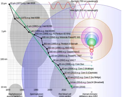
Figure 1.1. Shrinking of computer chip length scales with time. Perfect exponential shrinking law, as predicted by Moore, is shown with green line. Adapted from ref. [9]. .. 2
Figure 1.2. Schematic representation of three epitaxial growth pathways, starting from one monolayer of coverage to increasing coverage. Taken from ref. [10]. ... 4
Figure 1.3. (a) InAs dots on GaAs (scale 100 nm). Taken from ref. [11] (b) Pyramid/hut (P) and dome (D) nanoclusters of Ge/Si (30% Ge) on Si (scale ~10 nm). Taken from ref. [12] (c) Ge hut cluster on Si (scan area is 40 nm × 40 nm and island height is 2.8nm). Taken from ref. [13]. ... 4
Figure 1.4. (a) Bulk material with no quantum confinement and a continuous density of energy states (b) Quantum well, a material with one-dimensional quantum confinement, and a reduced energy density of states (c) Quantum wire, a material with two-dimensional quantum confinement, and a further reduced energy density of states (d) Quantum dot (QD), or three dimensionally quantum confined material, with delta function for energy density of states. Taken from ref. [21]. ... 6
Figure 1.5. (a) Si0.50Ge0.50/Si superlattice with ATG undulations. Taken from ref. [27] (b) Ge dots aligning with undulations in Si/SiGe superlattice. Taken from ref. [28] (c) Bright Ge islands grown on vicinal Si (001). Taken from ref. [23] (d) Lithography/RIE (Reactive Ion Etching)-created pits lead to patterned Ge dots. Taken from ref. [24] (e) Atomic Force Microscopy scan and schematic of Ge dots on Si surface with patterned oxide. Taken from ref. [25] (f) Patterned Ga ion implanted seen to guide nucleation sites for Ge islands on Si. Taken from ref. [26]. ... 9
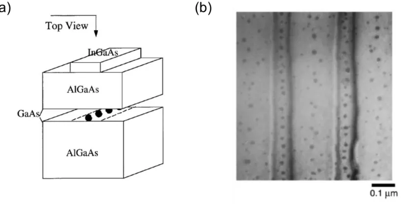
Figure 1.6. (a) Schematic of InGaAs lines on the surface of the AlGaAs/GaAs heterostructure (b) Plan view transmission electron microscopy micrograph of an array of As particles below stressor lines. Taken from ref. [29]. ... 11
Figure 1.7. A nanopillar template is applied to a SiGe wafer (a,b). During annealing, larger Ge atoms preferentially diffuse away from areas of compression, creating patches of enhanced Si content (c). ... 12
Figure 2.1. (a) Schematic representation of assembly used to create patterned stress fields in a SiGe substrate. (b) SEM image of Si nanopillar array used to apply a patterned stress field to the SiGe substrate. (c) Steps in the stress transfer process: (i) place Si nanopillar indenter array on top of SiGe substrate, (ii) press the indenters against the substrate, and (iii) thermally anneal the stack under patterned stress field. ... 16
Figure 2.3. Atomic percentage of Si and Ge near the surface of indented SiGe substrate. Case (a): T = 1000 ºC, P = 35 GPa. Case (b): T = 1000 ºC, P = 45 GPa. Case (c): T = 1000 ºC, P = 40 GPa. Inset TEM images show (a) complete Ge depletion with elastic deformation, (b) no discernable compositional change with plastic deformation, and (c) intermediate case with highly localized Ge depletion. ... 21
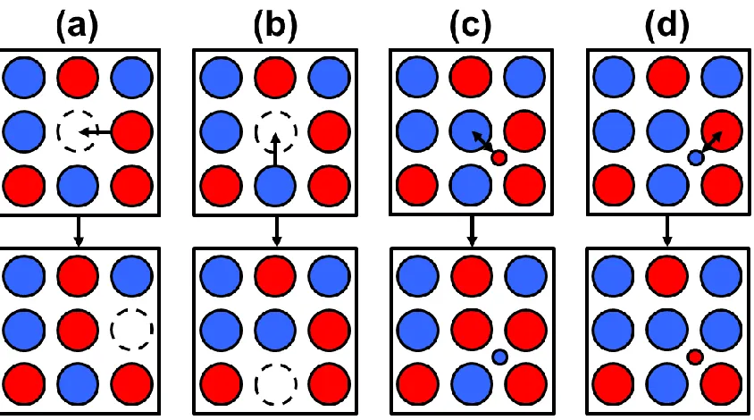
Figure 3.1. Schematic of defect mediated atomic diffusion. Red atoms represent Si and blue atoms represent Ge: (a) vacancy-enabled Si motion, (b) vacancy-enabled Ge motion, (c) Si interstitial ‘kicks out’ a Ge atom creating a Ge interstitial, and (d) a Ge interstitial kicks out an Si atom creating an Si interstitial. ... 24
Figure 3.2. Concentration (a), diffusivity (b), and transport capacity (c) of neutral vacancies in silicon as a function of temperature. ... 26
Figure 3.3. Schematic of different computational techniques and accessible length and time scales. ... 28
Figure 3.4. (a) Schematic of applied surface strain field to generate stresses in substrate (b) xz-cross section of film showing compositional evolution as a function of sweeps. Smaller B atoms (light gray) preferentially aggregate in regions of high stress. Taken from ref. [30]. ... 30
Figure 3.5. Schematic of KMC algorithm ... 32
Figure 3.6. (a) Snapshot of vacancy clusters in silicon. Taken from ref. [44] (b) Single atom-thick island distribution (squares) during deposition on a patterned surface predicted by KMC. Here, the binding energy between substrate and adatom varies sinusoidally in x and y. Left – configuration at coverage 0.15 (T=400K); right – configuration after coarsening at T=800K. Taken from ref. [45] (c) Dewetting and islanding seen after three monolayers of growth. Taken from ref. [48] (d) Ripening of islands of Al on Al surface. Taken from ref. [50]. ... 35
Figure 3.7. (a) Domain decomposition into nine regions, with shaded “ghost” regions and solid “skin” regions for the central domain. The ghost region of one domain is the skin region of its neighbor (b) Parallel efficiency, versus number of CPU cores (PEs), defined as the ratio of CPU time on one core for N rates divided by the CPU time on PE cores for PE×N rates., for some model diffusion systems. Taken from ref. [51]. ... 36
Figure 3.8. Temporal evolution of phase aggregation in the presence of periodic applied strain. The red regions are negatively (tensile) strained precipitates, which is equivalent to smaller atoms aggregating in regions of imposed compression. Taken from ref. [69]. 41
Figure 4.2. (a) Schematic of LKMC domain comprised of cubic cells measuring Lcell in length and containing ntot Si and/or Ge atoms (b) Schematic of coarse-graining atomic configurations in cells. Red atoms represent Si and blue atoms represent Ge (c) Schematic of LKMC switch move. In the depicted exchange, a Ge atom is moving from the lower left to the lower right and an Si atom is moving from the lower right to the lower left. ... 55
Figure 4.3. Energy change for an SiGe identity flip in a 64-atom cubic SixGe1-x cell at different combinations of stress state and composition. (a) Uniaxial stress, (b) biaxial stress, and (c) hydrostatic stress. GeSi identity flips lead to equal and opposite energy changes. ... 61
Figure 4.4. Schematic of simulator algorithm using stress field computed from molecular statics. See text for details. ... 67
Figure 4.5. Binned atomistic pressure (circles) and quadratic fit (line, R2 > 0.999) as a function of distance normal to the contact point between the 50-nm-diameter cylindrical indenter and substrate, predicted by quasi-static indentation of a Si0.8Ge0.2 slab. The annular segments used to bin the pressures are 3 nm wide (centered below the indenter)
and 0.5 nm thick. The profile shown here corresponds to an indenter applied with a
force per length of 6.57 x 10⁻⁸ N/nm. ... 69
Figure 4.6. Maximum contact pressure obtained from energy minimization of an atomistic model (red line), along with the continuum analysis fit to the data (green line), for the indentation of a Si0.8Ge0.2 film using a 25 nm (radius) cylindrical indenter. See text for details. ... 71
Figure 4.7. (a) Stress (σzz) in the xz-plane generated by an infinite (in y) cylindrical wire indenter of diameter 80 nm, corresponding to a maximum contact pressure of 15 GPa, mapped onto the undeformed domain. Result from plane strain calculation assuming isotropic elasticity. (b) FEM mesh used to generate the stress field in (a) (c) Indenter force versus maximum contact pressure for 80 nm-diameter, infinitely long, cylindrical indenter against Si0.8Ge0.2. Blue line – anistropic elasticity, green line – isotropic elasticity, black dashed line – Hertz contact model. ... 74
Figure 4.8. Simulated Ge concentration profiles (a,b) in an initially uniform Si0.8Ge0.2 film following 3 hours of thermal annealing at 1000 °C under stresses (c,d) induced by contact with an 80 nm-diameter spherical indenter with maximum contact pressure of 9 GPa (a,c) and 35 GPa (b,d). Note that (a)-(d) show an xz-plane of the three-dimensional simulation domain taken at the center of contact in y; this convention is used throughout the Chapter. (e) Scanning electron microscopy (SEM) image of the Si nanopillar indenter array used in the experiments reported in Chapter 2. (f) Near-surface (see text) Ge concentration as a function of x-position. Black line—experimental EDS measurement with maximum contact pressure ~35 GPa (based on Hertz contact model), blue line— LKMC with maximum contact pressure 9 GPa, red line—LKMC simulation with
35 GPa. All LKMC simulations performed with coarse cell size Lcell=6.56 nm. Note that the simulation profiles in (f) represent two copies of the actual simulation domain. ... 78
Figure 4.9. Ge concentration profiles in the top layer of coarse cells of a Si0.8Ge0.2 substrate subjected to a 80 nm-diameter cylindrical wire indenter following 3 hours of annealing at 1000 °C. The maximum contact pressure was 18 GPa. Individual profiles obtained with different LKMC coarse cell sizes: Gray—Lcell=2.19 nm (512 atoms/cell), blue—Lcell=3.28 nm (1,728 atoms/cell), orange—Lcell=4.37 nm (4,096 atoms/cell), pink—
Lcell=6.56 nm (13,824 atoms/cell). Note that all wire indenter simulations are based on
two-dimensional LKMC domains that are a single cell thick in the y-direction. ... 80
Figure 4.10. Steady-state Ge concentration profiles in top layer of LKMC cells of an initially uniform Si0.8Ge0.2 film subjected to an 80 nm-diameter wire indenter (maximum contact pressure of 18 GPa) and annealed at 1000 °C. Red line—elastic constants corresponding to initial (uniform) composition, blue line—with lattice mismatch and elastic constants corresponding to spatially-varying steady-state compositional profile. 81
Figure 4.11. Simulated Ge concentration profiles (a,b) in an initially uniform Si0.8Ge0.2 film following 3 hours of thermal annealing at 1000 °C under stresses (c,d) induced by contact with (a) an 80 nm-diameter spherical indenter, and (b) an 80 nm-diameter wire indenter, both with maximum contact pressure of 18 GPa. (e) Compositional profiles in the top layer of cells; orange line—wire indenter, blue line—spherical indenter. As noted earlier, the spherical indenter LKMC simulation results represent an xz-slice taken from a three-dimensional domain, while the wire indenter simulations are two-dimensional. ... 83
Figure 4.12. Ge concentration profiles (a,b) in an initially uniform Si0.8Ge0.2 film following 3 hours of thermal annealing at 1000 °C under stresses (c,d) induced by contact with an 80 nm-diameter wire indenter (maximum contact pressure 18 GPa) with inter-wire spacing of (a,c) 105 nm, and (b,d) 210 nm. (e) Compositional profiles in the top layer of cells; orange line—105 nm pitch, blue line—210 nm pitch. ... 85
Figure 4.13. (a)-(d) Sequence of snapshots of Ge concentration fields in SiGe film during annealing at 1000 °C under a spherical indenter of diameter 80 nm and maximum contact pressure 21 GPa, (e) Ge concentration profile in top layer of LKMC cells after 0s (grey), 14s (blue), 74s (orange), 1 hour (pink) and 3 hours (red). ... 88
Figure 4.14. (a) Ge concentration in the top layer of LKMC cells in an initially uniform Si0.8Ge0.2 film following annealing for variable times under the action of a 80 nm-diameter wire indenter (maximum contact pressures 18 GPa). Annealing times are 30 min at 1050˚C (pink), 180 min at 1000˚C (blue), 700 min at 950˚C, and 3300 min at 900˚C. (b) Arrhenius plot of annealing time to reach set patterning extent versus inverse temperature; circles are simulation data, dashed line is the Arrhenius fit. ... 89
nm and maximum contact pressure 21 GPa (See Chapter 4). Green is net event LKMC and red is full LKMC. ... 96
Figure 5.2. (a) schematic of changing entirely high resolution region of LKMC domain to variable resolution (b) schematic of exchanges between regions comprised of two different cell sizes (c) schematic of exchanges between equally size cells (d) sample LKMC grid. See text for details. ... 98
Figure 5.3. Example mesh and geometry used to solve stress problems in this Chapter. ... 100
Figure 5.4. Meshes used in mesh refinement study (left), along with σzz in xy-plane at top substrate surface in z (right)for (a) coarsest mesh (b) intermediate mesh (c) finest mesh. ... 103
Figure 5.5. (a) Composition and (b) standard deviation in top layer of LKMC cells after 3 hours of annealing at 1000 °C after solving stress problem using mesh in Figure 5.4(a) (red), mesh in Figure 5.4(b) (blue), mesh in Figure 5.4(c) (green). ... 104
Figure 5.6. (a) Sample indenter geometries, ranging from a spherical cap (radius of curvature of cap (Rcap) = indenter radius (R)) to an indenter with Rcap >> R (b) Two indenters separated by pitch, p. ... 106
Figure 5.7. Compositional profiles after thermal annealing of a Si0.8Ge0.2 substrate under the action using a spherical indenter tip measuring (in Rcapand R) (a) 25 nm (b) 100 nm (c) 125 nm (d) 150 nm (e) 175 nm (f) 200 nm, at a cubic p of 210.3 nm. ... 108
Figure 5.8. Compositional (a-b) and stress (c-d) profiles after thermal annealing of a Si0.8Ge0.2 substrate at 1000 °C using a spherical indenter tip with Rcap = R = 125 nm at a cubic p of (a,c) 105.2 nm (b,d) 210.3 nm. ... 110
Figure 5.9. Compositional (a-b) and stress (c-d) profiles after thermal annealing of a Si0.8Ge0.2 substrate at 1000 °C using a spherical indenter tip with Rcap = R = 125 nm at a p of 210.3 nm with an (a,c) cubic indenter array (b,d) hexagonal indenter array. ... 111
Figure 5.10. Stress field during thermal annealing of a Si0.8Ge0.2 substrate under the action of an indenter with R = 125 nm at a cubic p of 210.3 nm for 3 hours at 1000 °C for (a) Rcap= 125 nm (b) Rcap = 500 nm (c) Rcap= 1000 nm (d) Rcap= 2000 nm. ... 113
Figure 5.11. Compositional profile after thermal annealing of a Si0.8Ge0.2 substrate under the action an indenter with R = 125 nm at a cubic p of 210.3 nm for 3 hours at 1000 °C for (a) Rcap = 125 nm (b) Rcap = 500 nm (c) Rcap= 1000 nm (d) Rcap= 2000 nm. ... 114
Figure 5.13. Compositional profiles after thermal annealing of a Si1-xGex substrate under the action of a spherical indenter tip with Rcap= R = 125 nm at a cubic p of 210.3 nm, with the substrate compositions of (a) 20% Ge (b) 40% Ge (c) 60% Ge (d) 80% Ge. .. 116
Figure 5.14. (a) Stress before (left) and after (right) rotation of cylindrical indenter after 3 hours of thermal annealing of a Si0.8Ge0.2 substrate annealed at 1000 °C (b) compositional profile at time of rotation. ... 118
Figure 5.15. Compositional profiles after rotating indenter field and continuing the thermal anneal at 1000 °C for (a) 1 minute (b) 10 minutes (c) 1 hour (d) 3 hours. ... 119
Figure 6.1. (a) Film dimension changes upon formation of vacancy (b) Film dimension changes upon formation of interstitial (c) Film dimension changes upon migration of vacancy (d) Film dimension changes upon migration of interstitial. See text for details125
Figure 6.2.
tr
(
V
f)
V
r
(positive for vacancies) for (a) Si vacancies and (b) Si interstitials. Red = T3, yellow = EDIP, green = SW, light blue = T-EA, dark blue = MEAM, black dashed line = average of literature values, black solid line = fit to data from ref. [78]. ... 136Figure 6.3.
tr
(
V
m)
for (a) vacancies and (b) interstitials. Red = T3 (Si), yellow = EDIP, green = SW, light blue = T-EA, dark blue = MEAM, purple = T3 (Ge). ... 142Figure 6.4. ( ( m)) /
d tr V dTfor (a) vacancies and (b) interstitials. Red = T3 (Si), yellow = EDIP, green = SW, light blue = T-EA, purple = T3 (Ge). ... 144
Figure 6.5. Values of DC P( ) /DC(0) under hydrostatic stress for (a) vacancies and (b) interstitials, for silicon and germanium as computed in this work. Red = T3(Si), purple = T3(Ge), yellow = EDIP, green = SW, light blue = T-EA, dark blue = MEAM. Diffusion is isotropic under hydrostatic stress [32]. ... 147
Figure 6.6. Values of DC001(σ)/DC(0) under biaxial stress, 1122 , 33 0, for
(a) vacancies and (b) interstitials, and values of DC100(σ) /DC(0)DC010(σ) /DC(0) for (c) vacancies and (d) interstitials, for Si and Ge as computed in this work. Red = T3(Si), purple = T3(Ge), yellow = EDIP, green = SW, light blue = T-EA, dark blue = MEAM. ... 148
Figure 6.7. Values of DC001(σ)/DC(0) under uniaxial stress, 33 , 11220 , for
(a) vacancies and (b) interstitials, and values of DC100(σ) /DC(0)DC010(σ) /DC(0) for (c) vacancies and (d) interstitials, for Si and Ge as computed in this work. Red = T3(Si), purple is T3(Ge), yellow = EDIP, green = SW, light blue = T-EA, dark blue = MEAM. ... 149
contact pressure of 18 GPa) and annealed at 1000 °C in Chapter 4: red line – , blue
line – , and green line – . ... 156 zz
xx
Introduction
Chapter 1.
At the heart of all electronic and optoelectronic devices fabricated on
semiconductor substrates are abrupt compositional transitions. Such transitions may be
the result of the joining of two dissimilar materials [1], the growth of one material onto a
substrate of another [2], or be created in a single material that is compositionally altered
in a spatially varying manner. An example of the latter case is the ubiquitous silicon p-n
junction which is formed by doping adjacent regions in a pure silicon wafer with
electron-deficient (e.g., boron) and electron-rich (e.g., arsenic) chemical species [3].
The creation of compositional transitions at very small length scales may be
regarded as the essential goal of conventional microelectronic device processing. Here,
lithographic patterning, in which a masking material is used to create highly structured
apertures for introducing dopants [4], is combined with some means of introducing the
various dopant species into the semiconductor substrate, typically by diffusion [5] or ion
implantation [6] followed by thermal annealing. This sequence of steps is often combined
with deposition of multiple layers of material on the base substrate in order to build
increasingly complex structures [7]. This overall strategy is a classic example of so-called
‘top-down’ processing whereby the device features are built using (lithographic) patterns
at the same scale as the features.
The robustness of this approach in the face of continuously shrinking device
feature lengths, as originally predicted by Gordon Moore [8], has been truly
remarkable—as shown in Figure 1.1, todays devices are fabricated with features
prematurely predicted for a number of years, it is inevitable that the current materials
and/or approaches to semiconductor device fabrication will have to evolve. In this regard,
much research emphasis has been placed on the notion of ‘bottom-up’ fabrication,
whereby spontaneous self-organization or self-assembly is driven and guided to produce
structures that are otherwise inaccessible with traditional top-down techniques. The
realization of this goal will not only extend the life of Moore’s law scaling, but is
expected to make feasible the fabrication of a host of new electronic and optoelectronic
devices.
A well-studied example of this type of process is the spontaneous formation of
well-defined, three-dimensional islands observed during heteroepitaxial deposition (by
any technique, such as molecular beam epitaxy (MBE), chemical vapor deposition
(CVD), or physical vapor deposition (PVD)) of structurally similar, but lattice
mismatched materials, such as semiconductors (e.g., Ge on Si or InAs on GaAs) and
metals (e.g., Au on Ag). Generally, the atomistic details of the heteroepitaxial deposition
process are strongly influenced by the degree of lattice mismatch, which creates misfit
strain and increases the energy of the system. At low levels of mismatch, the deposited
adatoms fully wet the surface and lead to layer-by-layer, or Frank van der Merwe, growth
(Figure 1.2(a)); an example of this type of growth is observed in the Ag/Au heterosystem.
At high degrees of mismatch, no wetting is possible and the deposited species
immediately forms three-dimensional islands directly on the substrate with a very wide
size distribution; this is the so-called Volmer-Weber growth mode (Figure 1.2(b)). In
between these extremes, at moderate levels of lattice mismatch, a wetting layer is formed,
upon which further deposition leads to the formation of three-dimensional islands with
relatively good size and spatial distribution uniformity—this is known as the
Stranski-Krastanov (SK) growth mode (Figure 1.2(c)). It has been observed and studied in a
Figure 1.2. Schematic representation of three epitaxial growth pathways, starting from one monolayer of coverage to increasing coverage. Taken from ref. [10].
Figure 1.3. (a) InAs dots on GaAs (scale 100 nm). Taken from ref. [11] (b) Pyramid/hut (P) and dome (D) nanoclusters of Ge/Si (30% Ge) on Si (scale ~10 nm). Taken from ref. [12] (c) Ge hut cluster on Si (scan area is 40 nm × 40 nm and island height is 2.8nm). Taken from ref. [13].
Scientific interest in the semiconductor islands formed by SK heteroepitaxial
growth stems from their potential use as three-dimensionally quantum confined
which determines the available electron energy states, is altered such that electrons can
only occupy certain energy levels, restricting the energetic density of states (See Figure
1.4). The restriction increases as the dimensionality of confinement increases: quantum
wells (Figure 1.4(b)) exhibit one dimension of confinement, quantum wires (Figure 1.4
(c)) exhibit two dimensions of confinement, and quantum dots (Figure 1.4(d)), exhibit
confinement in all three dimensions. While confinement in each dimension leads to some
discretization of the bulk material density-of-states, three-dimensional confinement is
particularly exciting because the electronic density of states of QDs are fully discrete and
open up the possibility for creating devices with new capabilities, such as quantum
encryption and quantum computing [14-17]. Although a robust way to produce large
arrays of highly uniform and addressable quantum dots has not yet been demonstrated,
quantum wells are in routine use in a variety of optoelectonic devices such as lasers [18],
infrared photodetectors [19], and solar cells [20]. This is because while, it is quite
straightforward to modulate the composition of deposited layers in the direction of
growth to produce a sequence of thin layers of material with differing electronic band
structures, it is much more difficult to achieve this modulation in the lateral directions
Figure 1.4. (a) Bulk material with no quantum confinement and a continuous density of energy states (b) Quantum well, a material with one-dimensional quantum confinement, and a reduced energy density of states (c) Quantum wire, a material with two-dimensional quantum confinement, and a further reduced energy density of states (d) Quantum dot (QD), or three dimensionally quantum confined material, with delta function for energy density of states. Taken from ref. [21].
The fundamental challenge of creating highly uniform arrays of QDs on
semiconductor substrates has attracted a large amount of attention. In general, approaches
to increase size and spatial uniformity have been aimed at overcoming the inherently
random or stochastic nature of island nucleation by prepatterning the surface in some
manner to create preferential island nucleation sites. Selected examples are shown in
Figure 1.5. In (a), it is observed that an Si1-xGex layer grown on Si roughens, leading to
undulations in the adlayer, due to the Asaro-Tiller-Grinfeld (ATG) instability in the
system [22]. The ATG instability arises from a competition between surface energy and
elastic (mismatch) energy. Ge atoms in Si1-xGex migrate toward the peaks of the
undulations to reside in regions with a lattice parameter closest resembling Si1-xGex [22].
These “stacked” undulations are seen to guide the nucleation of Ge SK growth on the
surface of the superlattice (e.g., Figure 1.5(b)). A second approach to directing Ge SK
growth deposited Ge on a Si surface that contained steps, as islands are seen to
preferentially nucleate at the step locations [22]. In one example of this approach, miscut
Si (001) is used as a substrate [23]. A Si buffer layer is then grown on the substrate,
leading to a faceted surface with different orientations ((001) and (11x), x=8-10), with the
(001) facets being the preferred island nucleation location. Subsequent deposition of Ge
leads to dots nucleating in an ordered fashion (Figure 1.5(c)).
Another study employed surface “pits” generated in the substrate, which serve as
preferential nucleation sites [24]. Here, a two dimensional array of holes in a (001) Si
substrate was created via lithography and reactive ion etching, followed by a buffer layer
of Si. Upon deposition, Ge islands are seen to nucleate in a two-dimensionally ordered
manner (Figure 1.5(d)). A second lithographic surface prepatterning approach [25]
(Figure 1.5(e)) used patterned lines of oxide on Si (001) as a substrate. In this case, Ge
islands were observed to nucleate preferentially in alignment with the Si stripes.
Finally, altering the surface chemistry of the substrate can yield desirable control
over the dot formation process. One study used Ga ion implantation into an Si(100)
surface to create preferential nucleation sites for Ge island nucleation [26]. The
subsequently nucleated dots are seen to be very well ordered (Figure 1.5(f)).
These surface prepatterning approaches are all at least somewhat successful at
achieving spatial and size uniformity of islands formed during SK growth. However, it is
usually a strongly driven process, making near-perfect uniformity in island size and
distribution virtually impossible to achieve. In addition, given the strong driving force
1.1 Surface Stress Mediated Patterning of Compositional Rearrangement
As discussed in the preceding section, the numerous experimental studies aimed
at controlling Stranski-Krastanov growth of discrete islands on a semiconductor surface
are limited by the highly driven nature of nucleation during the island formation process.
A novel variation on the general theme of stress-mediated compositional evolution to
form structures with potential quantum confinement properties was demonstrated in a
pioneering study by Hung and co-workers [29]. Here, a GaAs-based multilayer structure
was grown via MBE, in which a thin layer of GaAs containing an excess of As atoms was
sandwiched between two AlGaAs layers (see Figure 1.6(a)). Stripes of InGaAs were then
lithographically patterned onto the heterostructure. Since InGaAs has a larger lattice
constant than GaAs (7.1% larger for InAs), localized stress fields were generated within
the sandwiched GaAs layer. Upon annealing, precipitates were found first to nucleate
homogeneously within the sandwiched GaAs layer, but eventually coarsened
preferentially in regions below the stressor stripes (Figure 1.6(b)). Moreover, the size
distribution of the ordered precipitates was found to be reasonably narrow. These
observations are consistent with nature of the nucleation process, discussed in the
preceding section, along with the weaker driving conditions governing the growth and
coarsening processes that are more amenable to the influence of the patterned stress field
Figure 1.6. (a) Schematic of InGaAs lines on the surface of the AlGaAs/GaAs heterostructure (b) Plan view transmission electron microscopy micrograph of an array of As particles below stressor lines. Taken from ref. [29].
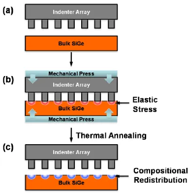
In this thesis, I computationally assess a new robust methodology to generate Ge
QCSs in SiGe, schematically illustrated in Figure 1.7. The approach involves subjecting a
uniform SiGe wafer, at relatively high temperature, to a spatially variable stress field
generated by indentation on the film surface (Figure 1.7(b)). Upon annealing, the larger
Ge atoms preferentially diffuse away from areas of high compression, leaving behind
regions of enhanced Si in the previously compressed patch (Figure 1.7(c)). Regions of
variable composition created by this procedure can serve as QCSs. Given that no
precipitates are nucleated in this approach, we hope to avoid many of the limitations
associated with previous demonstrations. To enable near-perfect scalability of the
procedure proposed here, we perform indentation using a reusable, albeit costly to
lithographically manufacture, indenter template. As far as residual surface modifications
patterning are seen to be well within the elastic regime, which will lead to substrates
containing a minimal amount of surface damage.
Figure 1.7. A nanopillar template is applied to a SiGe wafer (a,b). During annealing, larger Ge atoms preferentially diffuse away from areas of compression, creating patches of enhanced Si content (c).
The remainder of the thesis is structured as follows. Chapter 2 provides
results. Chapter 3 provides a discussion of the fundamental modeling challenges
associated with interdiffusion in the SiGe system and describes the most common
modeling alternatives used to address related problems. In Chapter 4, a coarse-grained
lattice kinetic Monte Carlo model is introduced and discussed in detail; this model serves
as the basis for all the validation and prediction studies carried out in this thesis. The
simulator, which is based on a similar model used to describe interdiffusion in biaxially
strained SiGe films, is parameterized using a large database obtained from numerous
literature studies, both experimental and computational. Chapter 4 also includes a
discussion of the impact of indentation strength and indenter size. Connections to the
experimental results discussed in Chapter 2 also are presented here.
Next, in Chapter 5, a detailed parametric analysis is presented of indenter
geometry, pitch, and annealing schedule, along with substrate composition, to determine
how to best generate compositional patterns that are consistent with quantum
confinement and therefore of greatest technological relevance. While many of the
parameters related to interdiffusion in SiGe are well-known (e.g., point defect diffusivity
in unstressed material as a function of temperature), the impact of stress on diffusion is
not well established at a quantitative level in the literature—this is perhaps the chief
modeling uncertainty in the results presented in Chapters 4 and 5. In Chapter 6, a
comprehensive analysis is presented of point defect diffusion under variable stress. In
particular, molecular dynamics simulations are used to estimate the so-called activation
volumes [32] for point defects using several popular empirical potentials. Finally, in
Chapter 7 conclusions are presented and some directions are proposed for future work
further optimize and extend the stress-patterning approach with the ultimate aim of
Demonstration of Stress-Directed Patterning in SiGe
Chapter 2.
2.1 Introduction
In this chapter, experimental verification of a new approach for creating
microscale compositional patterns in an SiGe wafer is presented. This work was
performed at the University of New Mexico by the experimental research group of
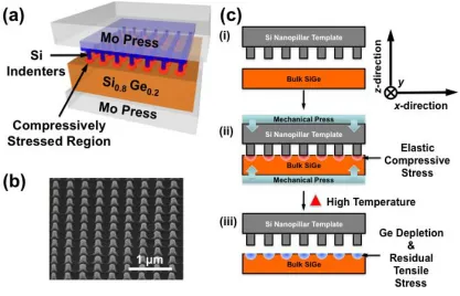
Professor Sang Han [33]. As briefly outlined in Chapter 1, a Si nanopillar indenter array
was used to apply a spatially patterned mechanical load onto the surface of a Si0.8Ge0.2
wafer and then the assembly was subjected to thermal annealing. As a result, the larger
Ge atoms migrated away from areas of compressive stress, leaving well-defined,
Si-enriched areas surrounded by bulk SiGe. The approach is depicted in Figure 2.1. The
various components of the experimental assembly are shown in Figure 2.1(a). A 2D array of Si
nanopillars (Figure 2.1(b)) and the SiGe substrate were pressed against each other in a
mechanical press consisting of top and bottom molybdenum (Mo) plates held together with 10
tungsten(W)-coated stainless steel screws. Each pillar was 80 nm in diameter and placed at a 200
nm pitch. The individual steps in the stress transfer process are shown in Figure 2.1(c). A
torque of 2-20 N-m was applied to each screw. The total applied force (F) was related to
the applied torque (T) according to [34]
s
N
F T
CD
, (2.1)
where Ns = 10, C = 0.2, and D = 0.00417 m represent number of screws, torque
coefficient [35], and nominal screw diameter, respectively. The maximum contact
between a spherical indenter top and a film plane. Details on the Hertzian contact model
are discussed in Chapter 4.
Figure 2.1. (a) Schematic representation of assembly used to create patterned stress fields in a SiGe substrate. (b) SEM image of Si nanopillar array used to apply a patterned stress field to the SiGe substrate. (c) Steps in the stress transfer process: (i) place Si nanopillar indenter array on top of SiGe substrate, (ii) press the indenters against the substrate, and (iii) thermally anneal the stack under patterned stress field.
Following the application of stress, the entire assembly was placed in a furnace at
elevated temperatures (900-1000 °C) for 3 hours to allow sufficient time for Ge atoms to
diffuse. After annealing, the furnace was brought to room temperature, and the
images were used to identify any material transfer from the Si indenters to the SiGe
substrate and any permanent plastic deformation. The SiGe substrate surface was further
characterized, using cross-sectional and scanning tunneling electron microscopy (XTEM
and STEM) to assess in more detail the crystalline structure below the indented regions.
Nano-probe energy dispersive spectroscopy (EDS) was also applied to map the
compositional redistribution near the SiGe substrate surface.
2.2 Experimental Findings
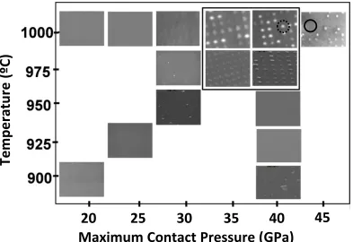
Figure 2.2 shows SEM images of post-annealed Si0.8Ge0.2 substrates as a function
of annealing temperature and maximum indenter contact pressure. Some of the SEM
images reveal visible residual post-anneal features on the Si0.8Ge0.2 substrates; these are
more prominent as the compressive stress and/or the temperature increases. Two different
features are highlighted in Figure 2.2. The dotted circle (T = 1000 °C, P = 40 GPa)
highlights a piece of Si left over from one of the indenter pillars as the indenter array was
separated from the Si0.8Ge0.2 substrate. The Si is likely to be evidence of bonding between
the Si nanopillars and Si0.8Ge0.2 substrate. The solid circle (T = 1000 °C, P = 45 GPa), by
contrast, appears to show a permanently indented area and is evidence of plastic
Figure 2.2. SEM images of Si0.8Ge0.2 substrates subjected to patterned stress fields and annealed for 3 hours, as a function of annealing temperature and maximum contact pressure. Each panel represents a region with dimension 1200 nm × 1200 nm.
A subset of the Si0.8Ge0.2 substrates was subjected to further analysis with XTEM
and EDS. Three different maximum contact pressures for constant annealing temperature
at 1000 ºC were considered: P = 35 GPa [Figure 2.3(a)], P = 45 GPa [Figure 2.3(b)], and
P = 40 GPa [Figure 2.3(c)]. For each case, EDS was used to sample a total of 45
uniformly spaced locations separated by 10 nm and sequentially denoted as (P1 to P45)
[see left-side inset XTEM images for each case] to infer a compositional profile near the
substrate surface. Each EDS measurement (P1 to P45) corresponded to a compositional
average over a 3×3×3 nm3 cuboidal region based on the electron beam diameter and
probing depth of EDS. Note that the irregularly-shaped objects present on the surface of
20
25
30
35
40
45
Maximum Contact Pressure (GPa)
Temperature
by EDS as being pure Si in composition, confirming that they were residual pieces of Si
nanopillars that became bonded to the SiGe substrate. Fortuitously, these residual Si
pieces were immensely useful as “markers” to precisely locate the regions where the
compressive stress is applied. For this reason, the high-stress cases were selected for EDS
analysis.
Case (a) in Figure 2.3 shows almost complete segregation of the larger Ge atoms
away from the compressively stressed areas below two distinct nanopillar contact regions
centered at locations P13 and P33. The width of the Ge-depleted regions is approximately
30 nm, although some Ge depletion is observed over a total distance of ~100 nm. No
visible defects or dislocations are found underneath the indented regions [see right-side
inset XTEM image of Figure 2.3(a)]. By contrast, the Ge segregation effect is almost
entirely absent for case (b), which, unlike case (a), exhibits a high density of line defects
up to a depth of about 30 nm from the surface [see right-side inset XTEM image of
Figure 2.3(b)]. These results suggest that only elastic deformation can induce Ge
diffusion and subsequent compositional variation, whereas plastic deformation actually
inhibits it. The intermediate indentation case (c) further supports this hypothesis. Here, a
low density of line defects (right-side inset) is shown to correspond to a microscopically
complex segregation pattern in the regions immediately below the indenter contact areas.
While it is very difficult to align the compositional fluctuations with specific microscopic
defect features, the highly localized nature of Ge segregation below the indenter contact
areas [e.g., note the absence of Ge depletion at P12 and P15, highlighted with rectangles
in (c)] strongly suggests that the segregation effect is controlled by the local
measurements were able to resolve the compositional profile down to length scales of at
Figure 2.3. Atomic percentage of Si and Ge near the surface of indented SiGe substrate. Case (a): T = 1000 ºC, P = 35 GPa. Case (b): T = 1000 ºC, P = 45 GPa. Case (c): T = 1000 ºC, P = 40 GPa. Inset TEM images show (a) complete Ge depletion with elastic deformation, (b) no discernable compositional change with plastic deformation, and (c) intermediate case with highly localized Ge depletion.
(a)
(b)
While elastic compression is required to drive the segregation effect, the results in
Figure 2.3 suggest that plastic deformation resulted in a near-complete relaxation of the
local elastic compression presumably by creep. This hypothesis is supported by the
permanent indentations observed on the substrate surface when both the temperature and
applied pressure were high (Figure 2.2). However, additional mechanisms may be
operational and cannot be ruled out. For example, line defects may locally impact the
concentration of the point defect diffusion mediators for Si-Ge exchange (e.g., by acting
as strong point defect sinks), thus inhibiting the stress-driven segregation process.
Moreover, plastic deformation of the nanopillars may be responsible for the reduced
elastic stress in the substrate during annealing. Note that for all cases considered here,
both Si and Si0.8Ge0.2 were well above their brittle-to-ductile transition temperatures (
~ 550
Si BDT
T °C [37]) where dislocation mobility is high. There also is the possibility of
surface melting; the low Ge concentrations used in this work suggest that surface melting
was not a factor, although higher Ge concentration substrates will likely limit the
annealing temperatures that can be applied.
2.3 Conclusions
In summary, we have described experiments examining a new approach for
establishing sharp lateral compositional profiles in the near-surface region of SiGe
substrates. Such profiles may provide useful building blocks for a new generation of
devices that take advantage of lateral quantum confinement. The approach relies on a
While these preliminary experimental results clearly demonstrate the feasibility of
mechano-patterning in the SiGe system, it will be difficult to evaluate and optimize the
process because of the costs associated with electron microscopy and the need for visible
surface features to locate the indentation sites. Consequently, a computational model is
essential to fully analyze the compositional segregation process. In the next Chapter, I
Review of Computational Approaches
Chapter 3.
Diffusion of Si and Ge atoms in bulk SiGe is entirely mediated by native point
defects (namely vacancies (V) and interstitials (I)). Both types of defects may assume a
variety of charge states, which will be addressed in the context of the model described in
Chapter 4, but the overall diffusional mechanisms they mediate are independent of
charge. Example point defect mediated diffusive processes are shown in Figure 3.1. In (a)
and (b), Si and Ge lattice atoms hop into an adjacent empty site in the lattice (i.e., a
vacancy), while the vacancy moves into the position previously occupied by the lattice
atom. In (c) and (d), an atom between lattice sites (an interstitial), exchanges position
with a lattice atom. In both cases, net motion of Si or Ge atoms has occurred; repetition
of this process leads to long range diffusion.
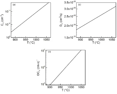
Point defect equilibrium concentrations in Si and Ge are extremely low: For
example, the concentration of neutral vacancies in Si is characterized by an Arrhenius
relationship [38]
0 exp
V
fV V
E
C C
kT
, (3.1)
with C0V = 2.5×1026 cm-3 and EfV = 3.9 eV. Figure 3.2(a) shows the vacancy
concentration over the range of annealing temperatures that are typical for the
stress-mediated compositional patterning process considered here. The corresponding atomic
fraction is in the range 10-11-10-14 (given an atomic density of ~5×1022 cm-3 [38]). The
diffusivities of point defects also are generally characterized by Arrhenius relationships.
For instance, the diffusivity of neutral vacancies in Si is given as [38]
0 exp
mV V V
E
D D
kT
, (3.2)
with D0V = 1×10⁻³ cm2/s and EmV = 0.4 eV. Figure 3.2(b) shows these diffusivities over
the same temperature range as shown for the equilibrium concentration. The product of
concentration and diffusivity, or DVCV in this case, is referred to as the transport capacity
of a defect species and is a direct measure of the ability of a defect to move atoms. For
neutral vacancies in Si, the transport capacity is shown in Figure 3.2(c) (based on the
Figure 3.2. Concentration (a), diffusivity (b), and transport capacity (c) of neutral vacancies in silicon as a function of temperature.
The preceding considerations immediately lead to the conclusion that a direct
molecular dynamics (MD) simulation of SiGe interdiffusion, especially over the length
and timescales that are relevant to the stress transfer process described in Chapters 1 and
2, is simply infeasible. This is the case even if relatively efficient empirical potentials are
employed to describe the interatomic interactions between silicon and germanium atoms.
Consequently, the appropriate simulation strategy must be based on some form of
coarse-grained representation. Shown in Figure 3.3 is an example of a hierarchy of
simulation representations beginning with quantum mechanical simulations (based on
varieties), to continuum simulations (in this context, referring mainly to phase field
simulations). In the ensuing discussion, we provide examples and brief introductions to
ig
u
re
3
.3
.
S
ch
ematic of
diff
ere
nt
comput
ati
ona
l t
ec
hniques a
nd
a
cc
essi
ble
leng
th
and ti
me sc
3.1 Metropolis Monte Carlo
Metropolis Monte Carlo (MMC) [39], while traditionally used to study systems at
the same resolution as MD, was used by Nieves and co-workers in a model of diffusion
under stress in which the individual point defect hops are coarse-grained, while an
overall atomic level description of diffusion in an alloy is maintained [30, 31]. In this
framework, a thin binary (A-B) film is created with imposed displacements in the z
-direction to impose an external stress field on the film (see Figure 3.4(a)). In all cases,
there is lattice misfit between A and B atoms, in order to drive compositional segregation.
Compositional evolution in the film is performed using the MMC algorithm, with
proposed moves comprised of nearest-neighbor atomic identity “switches,” in effect a
compound move of many of the elementary steps depicted in Figure 3.1. However, the
defects driving diffusion are implicitly accounted for in the simulation, thus increasing
the scales achievable via ordinary MD. The studies performed include a range of
potentials, from Lennard-Jones to MEAM, and all produce the same patterning behavior,
from which it is concluded that these types of simulations could be applied to a wide
variety of material systems, ranging from low to high misfit. The main physical limitation
of this approach results from the move basis for system evolution; while there is
qualitative progression of the compositional profile toward equilibrium (see Figure
3.4(b)), the dynamics of the process are not captured quantitatively. Given that there is no
guarantee that an anneal procedure has reached equilibrium for a given protocol, this
limits the predictive ability of the modeling proposed in this thesis. Computationally, this
that accurate energies are used in the MMC acceptance criterion. The ability to only
performing regionally local relaxations, does mitigate this limitation.
Figure 3.4. (a) Schematic of applied surface strain field to generate stresses in substrate (b) xz-cross section of film showing compositional evolution as a function of sweeps. Smaller B atoms (light gray) preferentially aggregate in regions of high stress. Taken from ref. [30].
3.2 Kinetic Monte Carlo Method
Kinetic Monte Carlo (KMC) (also known as dynamical Monte Carlo and in
certain contexts also as the Gillespie method [40]) is a stochastic approach developed to
model dynamics for systems that spend most of their time vibrating around potential
energy minima, only occasionally overcoming the energy barrier between basins [41],
creating a separation of time scales between vibrations and rare, basin-exiting events. For
fully atomically resolved MD simulations of systems in which this time scale separation
exists, e.g., for defects diffusing in a solid, one would integrate the equations of motion
for a system of atoms, most of the computational resources would be spent in one
potential energy minimum, and rarely, if ever, would a transition occur.
events are assumed to be independent Poisson processes. Under these assumptions, the
probability that the system remains in state i, is exponentially distributed [42]
( ) exp
i j ij
p t r t , (3.3)
where rij is the rate of leaving state i to go to state j. The average time to transition
between transitions is1 /rij. The total probability of the system remaining in state i can be written as the product of all of the individual probabilities [43]
( ) exp
i ij
j
p t r t
, (3.4)with the average time between transitions being 1 /
j ij r
. The probability density of thefirst escape time is written as
( ) exp
i ij ij
j j
k t r r t
. (3.5)A traditional KMC algorithm proceeds illustrated in Figure 3.5: All possible events are
enumerated, and a rate table is generated that includes every possibility. The time until
the next event is randomly chosen according to [42]
ln( )
d j ran
ij u t
r
, (3.6)with u being a uniformly distributed random number on [0,1]. Choosing the next event
time in this manner is consistent for a process with the rate constant of
j ij r
, given thedistribution in eq. (3.5) [42]. The identity of the event that takes place is chosen
often. After the chosen event is executed, the rate table is updated, and the algorithm
repeats.
Figure 3.5. Schematic of KMC algorithm
The primary limitation of KMC is that all possible events need to be known (and
specified quantitatively by rates) at all system states. Omission of important events
generally leads to incorrect simulation predictions. In contrast, the single physical input
to direct atomistic simulations such as MD or atomistic Monte Carlo is a potential
function that may be empirical or quantum mechanical. Once this is specified, no other
physical insight into the system behavior is required. In this context, KMC simulations
are conceptually similar to other approaches that require mechanistic input, such as rate
equation models based on ordinary or partial differential equations. However, as will be
available from molecular simulations, providing an advantage over other simulation
methods.
KMC models may be posed at arbitrary length scales. At one end of the spectrum,
the KMC representation may be fully atomically resolved, i.e., every atom in the system
is explicitly represented. Here, there are two broad classes of models: on-lattice and
off-lattice. On-lattice models, in which the atoms are constrained to a fixed set of sites
(usually lattice sites in a crystalline system) are easier to construct because of easier
enumeration of events and their rates. One example of an on-lattice KMC model was
developed by Dai and co-workers [44] to study vacancy aggregation in silicon. Assuming
that vacancies interacted up to the 8th-nearest neighbor shell, an 8 parameter model for
the vacancy hopping rates as a function of local environment was parameterized using
MD simulations. Figure 3.6(a) shows a vacancy aggregation configuration from a
simulation. As will be discussed at the end of this Chapter, the expense of fully
parametrizing a defect-mediated diffusion model was a factor in our choice of simulation
technique.
Other examples of on-lattice KMC models have been applied in atomic surface
morphological evolution studies. To illustrate the impact on surface morphologies of
strained interactions between mismatched adatoms and an underlying substrate, Mattsson
and Metiu [45, 46] imposed a periodic strain field on the surface of a substrate. This
strain field was supposed to mimic the elastic interactions between deposited atoms and
the surface, and the strain field was shown to induce the coalescence of the deposited
layer into islands (Figure 3.6(b)). Notably, and consistent with the discussion about the
![Figure 1.3. (a) InAs dots on GaAs (scale 100 nm). Taken from ref. [11] (b) Pyramid/hut (P) and dome (D) nanoclusters of Ge/Si (30% Ge) on Si (scale ~10 nm)](https://thumb-us.123doks.com/thumbv2/123dok_us/9331665.1467776/22.612.124.538.80.320/figure-inas-gaas-scale-taken-pyramid-nanoclusters-scale.webp)
![Figure 1.5. (a) Si0.50Ge0.50/Si superlattice with ATG undulations. Taken from ref. [27] (b) Ge dots aligning with undulations in Si/SiGe superlattice](https://thumb-us.123doks.com/thumbv2/123dok_us/9331665.1467776/27.612.157.497.70.593/figure-superlattice-undulations-taken-aligning-undulations-sige-superlattice.webp)