Low Potentials High-Performance Current
Mirror Using 32nm CMOS Process
Aman Kumar#1, Gurinder Pal Singh*2
#
*Electronics and communication dept., Chandigarh university , Punjab, India
Abstract- For the upsides of current style courses above the potential genre impediments, this postulation effort offers a different technique for current design’s designs base on substrate driving technology, appropriate for high speed and low power dissemination applications. Although previous technology is based on G-node was driven. In G-node technique signal are passes through the gate node. But, in the case of substrate driving method mass of the device is utilized to process the signal to get the benefit of low power. Adjusted design had been recreated in an exclusive 32nm CMOS prepare, utilizing Synopsis galaxy tool. Current comparator track had awed through current heartbeats going from 10-3A to 10-9A and its
quickness plus influence utilization had been recreated and estimated. At the point when made an examination with the prior detailed designs, our design accomplishes actual extreme rapidity of action as well as less potential utilization. For fast run i/p streams, the potential utilization of the recently enhanced current comparator is particularly inferior to the previously revealed designs. Simulation has performed on a 32nm process and obtained the result under short channel effects. We have considered the short channel effect during simulation so that dimensions are taken carefully for this technique.
Keyword — G-node, substrate driving Technology,
CMs (cm), Synopsis, C Designer Tool, Low energy .
I. INTRODUCTION
Current mode flag handling instigated in CMOS modernism has gotten growing enthusiasm for as long as decades. The course actual in current approach procedure involves very little region, expands a smaller amount of control dissemination besides accomplishes extraordinary action promptness. Additionally, numerous radars in SOC, for example, hotness beams, photograph sensors give current flag. In these requests also rapid information converters, for example, analog to digital converters, where the capacity of examination is a constraining part for exactness, clamor, and influence utilization details, the presentation of current mode arrangements is exceptionally alluring.
CMs completed by exploiting vibrant contraptions have originated to be all around consumed as a bit of directly made designs individually as biasing chunks
and as consignment gadgets for intensifier stages. The CM utilizes the rule that if the G-S results of double MOSFET devices are same, then the current flow across their D nodes ought to be consistent. The use of CMs in biasing can understand favored wantonness of design execution over combinations in authority source and heat [1]. N-type device CMs are utilized as current drives and P-type device CMs are utilized as current suppliers. Unmistakable CM designs [4] [5] [6] were shaped, each of the CM setups has their personal explicit expected utilize and usages in CMOS clear encouraged designs. There is a gathering of CM designs’, each of them developing their particular specific reasons for interest [7] [8].Bulk-driven is very important for the concern of threshold potentials [18]. It is used to reduce the threshold potentials further decrease power consumed by the design [19]. This Paper is dealt with: the brief outline is examined in the part I. The vital process of diverse CMs kind is depicted in section II. The proposed CM is discussed in part III. In region IV, outcomes of designs and association through diverse strategies are considered. Finally, section V has imparted the entire conclusion of this article.
II. DIVERSE CMS ORGANIZATION
A. Elementary CMs:
Figure-1 exhibits the Basic CM using N-type MOSFET devices as dynamic segments. T1 is diode related, obliging its D-Gate potential to null [1]. Therefore, device T1 works in the inundation area, which goes about as an unfaltering CS or allusion CS.
To fill in as a CM, both T1 and T2 are been vague MOSFET device. Slighting the network distance alteration affect, if the entryway wellspring of T2 is being uneven to a settled potential makes a reproduction of i/p current Iref at the D nodes of the
T2 device, implied by means of yield current. The improvement of yield current is particularly relating to the aspect proportion of the devices, point by point in the underneath particular condition.
=
=
1.
Consequences of traditional CM:After simulating the design under synopsis tool using 32nm we have taken dc sweep value between potentials source and the D node of the yield device T1.
Figure 2 Simulation result at the yield node
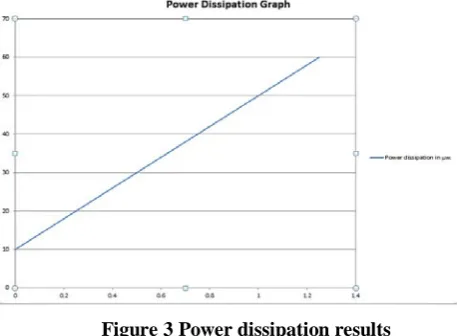
Figure 3 Power dissipation results
potentials are less. As we apply potential 0.8 – 1.2V we get power dissipation according to it.
B. Cascode CMs:
To attain extraordinary return challenge, cascode CM is expended. Outline 4 exhibits the cascode CM which practices N-type device as dynamic segments. The device T1, as well as T2, are organized as diode related, heading to works them in inundation area, which goes about as a relentless CS or references CS.
Figure 4 Cascode CM design
Important upsides of cascode CM are its capability to shield network length adjusts impacts. This is been accomplished by assembly D-S Potentials of T1 and T4 are built identical, so Iout constantly
traces Iref. To employment as a CM, both T1 and
T4 are preferred to be matching MOSFET devices.
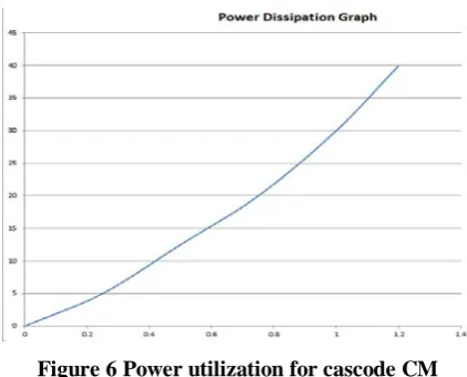
A. Outcomes of Cascode CM:
DC investigation has been performed using synopsis tool under a 32nm process. Figure-5 demonstrates the variety of yield current Iout
contrary to the sweep estimations of D potentials of T4.
Figure 5 Simulation result at the yield node
Figure 6 Power utilization for cascode CM
C. Improved Potential Separator Based CM
Figure-7 demonstrates potentials separator built CM. Enhanced design utilizes both devices to shape a potentials divider. N-channel device and P-channel devices are diode associated, creates the allusion potentials Vgs to inclination the
N-MOSFET device T2, which governor to switches the yield current. The i/p current Iref fashioned
through the overhead strategy is assumed as:
Assume that device T2 works in saturation way and therefore, the yield current develops
Figure 7 New potential separator based CM design
Figure 8 Simulation result at the yield node
Every MOSFET devices having a similar dimension proportion. Comparable Wilson CM, CMOS potentials separator founded CM utilized for small current biasing usages. This CM approaches less control utilization when contrasted with regular CMs.
Figure-8 demonstrates the dissimilarity of yield current Iout contrary to the scope estimations of
D-S potentials of T4, Vds2. As of the diagram,
it's been distinguished this enhanced CM is appropriate for lesser current biasing usages, for example, the dual phases intensifier.
III.PROPOSED WORK
The proposed CM is shown in figure 9 is established on the bulk driven cascode CM. It has used substrate driven approach. Every MOSFET devices having a similar W/L proportion. To reduce the threshold potentials aspect ratio is not a factor. Although to decrease the threshold potentials we can apply the signal on the bulk side and try to lessen the threshold potentials. Further, it will result in less power dissipation. In this we have use flipped potentials follower which has low power dissipation by its property and already have a high impedance. This is used with the cascode form of the device. Gate of the T1-T4 having fixed biasing potentials. And input signal is providing the bulk of the T2. Generally, yield has taken from the T3 but to amplify the yield of the device we have used the amplifier at the end of the yield impedance. It increases the trans conductance.
This method eliminates the threshold potential restraint of device commencing the signal track. Substrate-driving devices can operate at inferior power source potentials Vdd up to 1.2V.
Using less influence resource potentials, scheming equivalent circuit spending conformist G-node MOSFET devices is challenging.
. .
I
ref=
V
dd +Vgs1 – V
gs4/ R
Figure 9 Substrate driving high-performance CM design
Figure 10 Simulation result at the yield node
After simulating the design under synopsis tool using 32nm we have taken dc sweep value between potentials source and the D node of the yield device T5. The current source is having 10uA. We are getting the same current at the yield side with low power dissipation and high yield impedance.
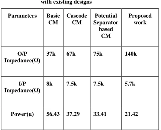
IV.COMPARISON OF CMS
Qualities and constraints of the traditional, Cascode, m o d i f i e d potentials separator based CM are equated with proposed CM design and the reflections are enlightened in the table.
Table I. Comparison between proposed designs with existing designs
Parameters Basic
CM
Cascode CM
Potential Separator
based CM
Proposed work
O/P
Impedance(Ω)
37k 67k 75k 140k
I/P
Impedance(Ω)
8k 7.5k 7.5k 5.7k
Power(µ) 56.43 37.29 33.41 21.42
V. CONCLUSION
The fundamental goal of this paper is to show the straightforward thought of planning substrate driving based CM, also provide correlation with the traditional and Cascode CMs. The proposed fresh CM is appropriate for low current biasing applications. Comparable the Wilson and Wilder CM designs, this planned CM can be utilized as a less current biasing design. On comparing this mirror with existing basic designs, it is found that it has enhanced yield resistance which is 2 times more than cascode CM and has a very less power dissipation. As CM are widely utilized in the operational amplifier as an active load. Due to the enhanced yield resistance, it can be used in Bio-medical applications where high yield impedance is required.
ACKNOWLEDGEMENT
REFERENCES
[1] Paul.R.Gray,Paul.J.Hurst, Stephen.H.Lewis and
Robert.G.Meyer, “Analysis and design of analog integrated designs”, by John Wiley & sons, Inc 1984.
[2] Behzad Razavi, "Design of analog cmosfet integrated
designs " , by Mc-Graw Hill.
[3] Vinamrata Yadav , Nikhil Saxena” A Darlington Pair Based
CMOS Two Stage Operational Amplifier at 32nm Technology”, International Journal of Engineering Trends and Technology 2017
[4] MULDER,J., and ROERMUND,A.H.M., “High swing
cascode MOSFET CM”, Ekec-Iron. Lett., 1996, 32, pp. 1251-1252
[5] Louis-Franc¸ ois Tangµ Ay, Mohamad Sawan, and Yvon
Savaria, "A very-high yield impedance CM for very-low potentials Biomedical Analog Design", IEEE-2008
[6] S. S. Rajput and S. S. lamar, “A high performance CM for
low potentials designs”, Proc. APCCASIIEEE,Tiwjin, China, pp. 170-173, Dec2000.
[7] Nikhita Tripathi, Sonal Soni , “Design of an Amplifier
through Second Generation Current Conveyor”,
International Journal of Engineering Trends and
Technology, 2013
[8] Hongtao Mu, Li Geng and Jun Liu ,“A high precision constant current source applied in LED driver”, IEEE-2011.
[9] H. Traff, "novel approach to high speed cmosfet current
comparators", IEEE Proceedings - Electronic
Letters,vol.28, No.3, 1992.
Chung-Yu Wu, Chih-cheng chen, Ming-Kai Tsai and Chih-Che Cho, “A 0.5µA Offset-Free Current Comparator
[10] For high precision current-mode signal
processing”, IEEE Proceedings – Designs amd Systems, Pages. 1829- 1832, Vol.3, 1991.
[11] Byung-moo Min and Soo-won Kim, “High
performance CMOSFET current comparator using resistive feedback network”, IEEE Proceedings - Electronic Letters, Pages. 2074-2076, vol.34, Issue.22, 1998.
[12] G.Palmisano and S.Pennisi, “Dynamic biasing for
true low-potentials CMOSFET class ab current-mode designs”, IEEE Transactions on Designs and Systems-II: Analog and Digital Signal Processing, Pages.1569-1575, Vol.47, Dec- 2000.
[13] Lu Chen,Bingxue Shi, and Chun Lu, “ A high speed/power
ratio continuous-time cmosfet current comparator”, IEEE Proceedings – Electronics, Designs and Systems, ICECS-2000, Pages. 883-886, Vol.2, Dec- 2000.
[14] D.Banks, and C.Toumazou, “Low-power
high-speed current comparator design”, IEEE Proceedings - Electronic Letters, vol.44, No.3, 2008.
[15] Soheil Ziabakhsh,Hosein Rad, Mohammad
Alavi-Rad and Mohammad Mortazavi, “ The Design of a low- power high-Speed current comparator in 0.35-ȝm CMOSFET Technology ”,IEEE Proceedings, 2009.
[16] C.B.Kushwah, D.Soni, and R.S.Gamad, “New design of CMOSFET current comparator”, IEEE Proceedings – ICETET -2009, Pages.125-129, Dec-2009.
[17] Chun Wei Lin,and Sheng Feng Lin, “ Low input impedance
current comparator using in pulse-width modulation ”, IEEE Proceedings – ICCE-2010,Pages.127-130
[18] Bhawna Aggarwal.et.al “Analysis of low potentials
bulk-driven self-biased high swing cascode CM”
microelectronics journal, 2012.
[19] Bhawna Aggarwal, Meenakshi, A.K. Gupta
![Figure-1 exhibits the Basic CM using N-type MOSFET devices as dynamic segments. T1 is diode related, obliging its D-Gate potential to null [1]](https://thumb-us.123doks.com/thumbv2/123dok_us/8588610.1720498/1.595.339.501.591.738/figure-exhibits-devices-dynamic-segments-related-obliging-potential.webp)