Design Simulation of Low Power Two
Stage CMOS Operational Amplifier
Sweta Km.Verma¹ Dr. Rajesh Mehra² ME Scholar, Associate Professor
Electronics and Communication Department of Electronics and Communication National Institute of Technical Teachers Training National Institute of Technical Teachers Training
And Research, Chandigarh And Research, Chandigarh [email protected] [email protected]
Abstract: This paper presents a comparative analysis of different parameters of general purpose two stage CMOS Operational Amplifier. The results presented are obtained through schematic level simulations using the Cadence virtuoso Design System and a standard 45nm and 90 nm CMOS technology process at operating voltage 1.8v . Simulation result confirms that the performance of the proposed 45nm technology is better and having lesser power dissipation as compared to conventional technology process.
Keywords: CMOS, Gain, Integrated Circuit, Operational Amplifier, Power dissipation.
I. INTRODUCTION
An Operational amplifier is a high gain electronic voltage amplifier with a differential input and usually a single ended output. An Op-amp produces an output voltage that is typically larger than voltage difference between its input terminals [1]. Operational Amplifiers represents one of the most useful and one of the most used building blocks for analog and integrated circuit such as A/D,D/A circuits, switched capacitor filters Instrumentation amplifier, signal generator, voltage regulators and non-linear analog operators[1][3][4].
In VLSI design, main goal is to reduce the power consumption in CMOS logic circuits. Low power and area efficient design are key goals for developer [3]. There are three sources of power dissipation Static Power, Short circuit power and Dynamic Power dissipation [5].
In this paper, the design and schematic level simulation of a two stage Op-amp are performed using common gate current buffer compensation technique. Output voltage, current and power dissipation are achieved using the Cadence Design System tool a standard 45nm and 90nm CMOS Technology process.
Fig.1 Block Diagram of Op-Amp [3][4]
Therefore the block can be removed. The gain provided by the input stages is not sufficient and additional amplification is required in most cases. An intermediate stage is used, which is another differential amplifier, driven by the output of the first stage. As this stage uses differential input unbalanced output differential amplifier, so it provide required extra gain [3]. The bias circuit is provided to establish the proper operating point for each transistor in its saturation region.
Lastly, we have the output Gain stage. It provides the low output impedance and larger output current needed to drive the load of op-amp or improves the slew rate of the op-amp. The purpose of the compensation circuit is lower the gain at high frequencies. It also maintains the stability of the circuit.
This paper composed these Section II Model used define the 2 stage amplifier and design optimization. Section III gives the Design methodology of op-amp and its specifications are briefly clarified, also gives the formula or calculation for designing of two stage CMOS Op-amp. Section IV gives the schematic design of Op-Amp. Section V presents the simulation results of the proposed op-amp, tables and graphs for optimization technique. Section VI results of this work and section VII gives the conclusion.
II. MODEL USED
A. Circuit Operation
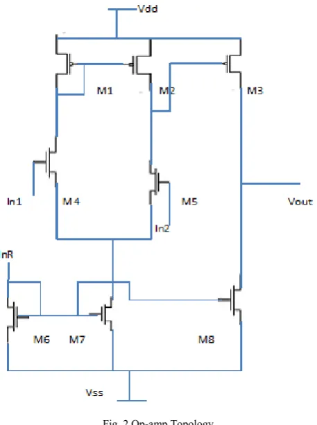
Fig. 2 Op-amp Topology
The topology chosen for this Op-Amp design Circuit, namely differential gain stage, second gain stage and bias strings. It was found that this topology was able to successfully meet all of the design specifications. Most importantly, M5 is biased by the gate to source voltage (VGS) set up by the VGS of the current mirror load as are the transistors M1 and M2 [3],[4].
B. Differential Gain Stage
Transistors M1, M3, M4, and M5 form the first stage of the op amp the differential amplifier with differential to single ended transformation. Transistors M4 and M5 are standard N channel MOSFET (NMOS) transistors which form the basic input stage of the amplifier. The gate of M4 is the inverting input and the gate of M5 is the non-inverting input. A differential input signal applied across the two input terminals will be amplified according to the gain of the differential stage.
The gain of the stage is simply the trans conductance of M5 times the total output resistance seen at the drain of M5. The two main resistances that contribute to the output resistance are that of the input transistors themselves and also the output
Resistance of the active load transistors, M1 and M2. Conversion from differential to single ended is achieved by using a current mirror (M1 and M2). The current from M4 is mirrored by M1 and M2 and subtracted from the current from M5. The differential current from M4 and M5 multiplied by the output resistance of the first stage gives the single-ended output voltage, which constitutes the input of the second gain stage.
C. Second Gain Stage
D. Bias String
The biasing of the operational amplifier is achieved with only four transistors. Transistors M6 and M7 form a simple current mirror bias string that supplies a voltage between the gate and source of M7 and M8. Transistors M8 and M7 sink a certain amount of current based on their gate to source voltage which is controlled by the bias string. M6 and M9 are diode connected to ensure they operate in the saturation region. Proper biasing of the other transistors in the circuit (M4-M3) is controlled by the node voltages present in the circuit itself.
III. DESIGNMETHODOLOGYOFOPAMP
The design methodology is based on common gate current buffer compensation Model [2][6].This model is based on concept of inversion level and the drain current can be split into the forward ( ) and reverse ( ) currents:
= - = ( - ) (1)
Where is the normalization specific current , and
and are inversion levels in forward and reverse direction respectively. These currents depends on the gate to source and gate to drain voltages respectively. If transistor operates in saturation region, we have :
,thus: = (2)
The normalization current is a function of the technology (3)
Where represents the charge mobility, gate-oxide capacitance per area, thermal voltage , n slope factor and transistor aspect ratio. The inversion level value signifies the transistor operation region in the following way: if 1, the transistor operates in weak inversion and if 100 the transistor operates in strong inversion region. If 1 100, the transistor operates in moderate inversion region [3] [5][6][7].
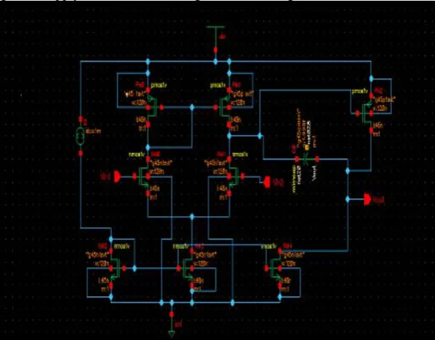
IV. SCHEMATICDESIGN
The design in this model is a two-stage Op-amp , it uses dual –polarity power supply so the signal can swing above and below ground supply. The schematic design is shown in figure 3.
The transistor level schematic is designed in Cadence Virtuoso Schematic editor for 45nm technology.
The PMOS and NMOS transistors used to build the schematic diagram are selected as per the specification given below in Table 1.
Parameter 45nm 90nm
NMOS PMOS NMOS PMOS
Length 45nm 45nm 100nm 100nm
width 120nm 120nm 120nm 120nm
Threshold 800nm 800nm 120nm 120nm S/D Metal 60nm 60nm 120nm 120nm
Table1.Specification of PMOS and NMOS V. SIMULATIONRESULTS
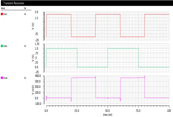
The result shows in Fig 4 is the transient response of the above schematic diagram obtained from fig 3.Transient response gives the idea that how fast Op-Amp will respond to input signal. This response is obtained after simulation and running of CMOS OP-Amp on Cadence Virtuoso design tool of GPDK 45nm technology.
Time is considered on X-axis and voltage is considered on Y-axis. Time is taken as 25ns, 75ns and 100ns. and are input voltages which is indicated with red And green color and their respective values are 1v and 1.8v.Output voltage is represented by magenta color and it varies between 380 mv to 60mv with respect to time.
Fig 4. Input and Output voltage response in 45nm Technology
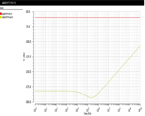
In fig 5 time is considered on X-axis and voltage is considered on Y-axis . and are input voltages which is indicated by green and Magenta color. Purple wave indicates the reference voltage which is 800mv.Both input voltages and is 1.8v .Output voltage is represented by blue line which is equal to 131mv. In Fig 6 Frequency is considered on Y-axis and voltage is considered on X-axis. Red line indicates input voltage which is -60dB.Yellow line indicates output voltage which is -180dB up to 10K Hz, between
Hz to Hz it is -188dB and again it increases and reaches to -110dB.
Fig 6.db20 response in 45nm Technology
Fig 7.db20 response in 90nm Technology
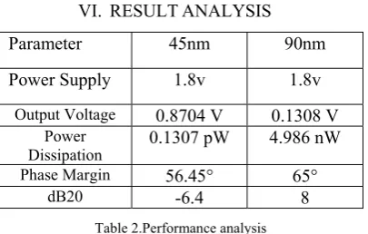
VI. RESULTANALYSIS
Parameter 45nm 90nm
Power Supply 1.8v 1.8v
Output Voltage 0.8704 V 0.1308 V
Power
Dissipation 0.1307 pW 4.986 nW
Phase Margin 56.45° 65°
dB20 -6.4 8
Table 2.Performance analysis
The above table shows the parameters of Op-Amp using GPDK 45nm and 90nm technology. These values are calculated by using calculator function on Cadence analog and digital system design tools. Important parameters of Op-Amp are calculated for a qualitative comparison between 45nm and 90 nm technology process. The output voltages are 0.8704 V and 0.1308 V at GPDK 45nm and 90nm technology. Power Dissipations are 0.1307pW at 45 nm and 4.986nW at 90nm technology process.
VII.CONCLUSION
The performance analysis of proposed model has been done in terms of power dissipation and output voltage. This design is compared with 90nm CMOS technology process. After analysis of the simulated result, it can be concluded that 45nm CMOS technology process is superior to conventional process. The Power dissipation has reduced to 0.1307pW as compared to 4.9860nW of conventional process. The output voltage is found to be increased 0.870V as against 0.1308V which makes the proposed design technology process more efficient.
ACKNOWLEDGEMENT
The authors are grateful to Dr. M. P. PUNIA Director NITTTR, Chandigarh for support throughout this research. The author would also like to thanks to Dr. Maytre, Professor and head, ECE department, NITTTR Chandigarh for helpful suggestions.
REFERENCES
[1] P R Pournima , “Design of Rail-to-rail Opamp in 90nm Technology,” IJSTE-Vol.1,Issue 2,Aug 2014,pp 38-44
[2] Aleksandar Pajkanovic , “ A 130 nm Operational Amplifier: Design and Schematic Level Simulation,”7th International Conference on ComputationalIntelligence, Communication Systems and Networks (CICSYN), 2015, pp.249-254.
[3] Siddharth, Mehul Garg, Aditya Gahlaut,”Comparative study of CMOS Opamp in 45nm and 180 nm Technology,”ISSN-2248-9622,Vol. 4,Issue 7,July 2014,pp 64-67.
[4] Amana Yadav , “Design of Two-stage CMOS Op-Amp and Analyze the effect of scaling,” International Journal of Engineering research and Applications (IJERA), Vol.2, No.5, Oct 2012, pp.647-654.
[5] Priyanka Sharma, Rajesh Mehra ,” True Single Phase Clocking based Flip-Flop design using Different Foundries” , International Journal of Advances in Engineering and Technology(IJAET), May 2014, pp.352-353.
[6] B. Razavi , Design of Analog CMOS Integrated Circuit. McGrow-Hill,2001.
[7] Neil H.E Weste , David Harris, Ayan Banerjee, “CMOS VLSI Design: A Circuits and Systems Perspective” ,Third Edition, 2007
Ms.Sweta Km. Verma: Ms.Sweta Km. Verma is currently pursuing her ME degree from National Institute of Technical Teachers’ Training & Research, Chandigarh, India. She has received her bachelor degree from Dr.K.N.Modi Institute of Engg & Technology Modinagar, India in 2007.Ms.Sweta has 6 years of Industrial and Teaching experience.