RELIABLE DATA SYNCHRONIZATION
IN GALS’ SOC
VIVEK E. KHETADE
Assistant Professor, Department of Electronic Design Technology Shri Ramdeobaba College of Engineering & Management, Rashtrasant Tukdoji Maharaj Nagpur university Nagpur, India
DR. S. S. LIMAYE
Professor, Department of electronics engineering, Jhulelal Institute of Technology
Rashtrasant Tukdoji Maharaj Nagpur university Nagpur, India [email protected]
Abstract
Synchronizer used for data synchronization posses non-zero probability of failure in Globally Asynchronous Locally synchronous System on Chip. It plays very crucial role in determining the reliability of system. Synchronizer is susceptible to metastability if asynchronous data changes in setup and hold time window. The output of synchronizer is indeterminate .This risk must be mitigated. In this paper structure of synchronizer is proposed for improved reliability. It determines change of data in the metastability window with signal setup start (SS) and hold end(HE) . To receive synchronised data, it samples synchronizer which is placed in parallel with operating synchronizer .This parallel placed synchronizer receives delayed data. This proposed architecture is modelled with VHDL and simulated with ModelSim SE6.2C for functional correctness. Asynchronous data rate is generated at varying frequency .MTBF is improved substantially with the increase penalty of one cycle.
KEYWORDS:
Data synchronisation, Globally Asynchronous Locally synchronous synchronizer (GALS), metastability, SOC.
1. Introduction
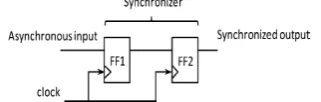
Data synchronization is required for transferring the data from one clock domain into another clock domain or when asynchronous data enters into synchronous clock domain on the same chip .This synchronization is performed by synchronizer. System-on-chip that consists of multiple clock domain connected through asynchronous interconnect are called globally asynchronous and locally synchronous Network-on chip (GALS-NOC). Frequency and phase of each synchronous module (IP core) is independent. Number of synchronizer is proportional to number of clock domain. Synchronizer is the gateway through which asynchronous input enter synchronous domain. Reliability of synchronizer is crucial for the reliability of SOC. When the data violates setup and hold constraints of the synchronizer, then it enters in to Metastable state, where we are unable to determine the state of output i.e. zero or one. Reliability of synchronizer is estimated based on probability that it enter into metastability and time to exit from metastability. Mean time between failures [1] for the two flip-flop synchronizer is expressed as
Failure (t) ≡ the synchronizer that became metastable at time 0 is still metastable at time t.W ≡ Danger window during a clock cycle: If the input data to a synchronizer changes during W, then the synchronizer is assumed to become metastable. FC ≡ sampling clock frequency T ≡ sampling clock cycle time. FD ≡ Frequency of changes in the input data. τ ≡ Resolution time constant of the synchronizer. This synchroniser is proved quite safe under some assumption
But there exist nonzero probability of occurrence of change of data in metastability window. Reliability of synchronizer depends on data rate, frequency of operation of synchronizer and performance parameter of synchronizer such as setup and hold window. These performance parameters are deteriorating with technology scaling, process, and voltage variation.
Various synchronizers are proposed over the decade Two flip-flop synchronizer (conventional), Jamb-Latch synchronizer, cascaded Flip-flop synchronizer, robust latch synchronizer, wagging synchronizer[2][3][4]. Various technique for data synchronization has been implemented which played with clock i.e. Pausible clock, stretchable clock ,data driven clock to make reliable data transfer across clock domain[5][6][7].Here we are suggested mechanism for metastability free data transfer where if data changes in window, then don’t sample the output of synchronizer rather delay the data and then sampled the parallel placed synchronizer. This work is little similar with data delay adaptive synchronizer [4] .This paper proposes the structure for metastability free data synchronization and its analysis. Paper is organised as follows. In section 2 principal of proposed architecture of delayed data synchronisation is explained with help of block representation. In section3 black box representation of synchronizer controller along with its hardware realisation is presented. Simulation and result analysis is discussed in section 4. Conclusion and Reference are given in section 5 and 6 respectively.
2.Proposed Architecture of delayed Data synchronisation
2 .1 Principal of operation with Block Representation
When data changes in the metastability window (sum of setup and hold time) with respect to the clock edge, then asynchronous data is not entered correctly in clock domain through synchronizer .The output of synchronizer may be unpredictable, it can be in the middle of zero and one. The effort is made to delay the data rather than any other parameter in clock domain. If the data changes in the metastability window then the output of synchronizer1a will not be taken in system, rather delayed data and synchronizer 1b will be taken. In this system, clock period is needs to be exactly calculated at input synchronizer. When clock edge is detected, delay of setup time and hold time for next clock cycle can be derived. Metastability window begin with start of setup time and ends with end of hold time shown in fig 2. The signal ‘ss’ is indicating the beginning of metastability window and the signal ‘HE’ indicates the end of metastability window. Whenever signal ‘ss’ becomes high, data change detection block will poll for the data change and continue till signal ‘HE’ is high. If in between the data changes then data change detection block will generate control signal. This control signal is used as select line of mux .Data will gets delayed by delay Tw and then sampled by synchronizer 1b. Data will be appearing correctly at synchronizer1b whereas synchroniser 1a will enter in metastability .It will not be selected by mux.
Data change detection is achieved with simple xoring of data. This pulse of data change is combined with ‘SS’ and ‘HE’ pulse to select the mux input line. Here we have assumed that synchronizer1a‘s output is indeterminate once the data changes in window. Synchronizer 1b received the data with delay of ‘Tw’ and naturally data will not change in the window. It will sample the data at next clock edge and we will get the synchronised data. This representation is shown in more explored way in fig 3 and waveform with their timing relation is given fig 5.
3. Synchronizer controller
The black box representation of the synchroniser controller is shown in fig 4 It is represented with one input i.e.clk and two output setup start (SS) and hold end (HE) with respect to rising edge of clock. With the predetermined delay, we are able to estimate the setup start and hold end for the next clock cycle. Setup time and hold time of the synchronizer is fixed once we selected the technology specific synchronizer.
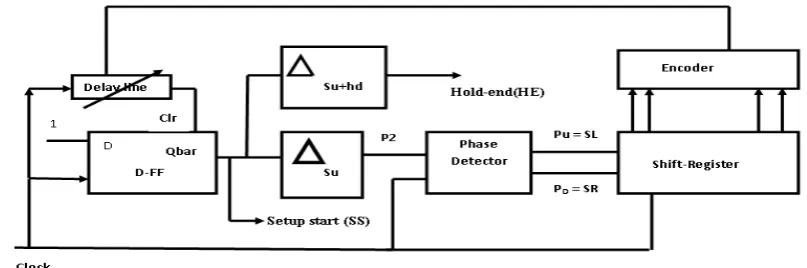
3.1Hardware Realisation of synchronizer controller
Synchronizer selection controller consists of Monoshot, Predetermined delay su and su+he, phase detector, shift register, encoder and delay line as shown in Fig 6. Monoshot is used to extend pulse width of the clock period up to setup start of the next clock edge. Predetermined delay su and su+he will offer the delay equal to delay of setup time and (setup + hold) time of synchronizer. Phase detector compares the phases of reference input clock and delay output. Comparisons yields a signal proportional to phase error i.e. pump up(pu) and pump down(pd) .These signals are connected to shift left(sl) and shift right(sr) of shift register. Shift register is loaded with one bit high. This bit is shifted left or right depending on phase error. Encoder will encode the output of synchronizer. Encoder ouput is used to select the delay from delay line. As long as there phase error, delay is adjusted. Once the phase error becomes zero, delay will get lock.
3.1.1 Monoshot & Delay line
Monoshot is used to increase pulse width of clock signal up to setup time of next clock cycle. This width is set with the help of delay line. This is connected to the clr pin of flip-flop as shown in fig 7. Fig 8 describes the implementation of Delay line [8] using multiplexer and delay element i.e. buffer .It offers the delay of 2nsec to 5nsec. This is implemented as Icells in altera PLD devices which provides delay of 1.5nsec.The minimal delay is achieved by select line of multiplexer i.e. when select lines are “0000”.The maximum delay is achieved when select lines of multiplexer are “1111”.
Fig 4 Black box representation of controller
Fig 6 Circuit diagram for synchronizer controller
3.1.2 Phase detector
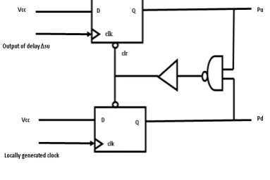
Phase detector received the input from clock and output of predetermined delay su. It compares their phase and generates the phase error signal as shown in Fig 9 and Fig 10. When both signals are aligned then there will not be any error signal. Delay of delay line is adjusted automatically so that there will no phase error. Phase detector is constructed with flipflop and NAND gates as shown in fig the clock of one of the flip-flop is drive through clock of local generator and clock of another flip-flop is derived from signal P2
4. Simulations and Result Analysis
System is model in VHDL and simulated on Modelsim 6.2C .C lock frequency is consider for simulation is 10 MHz. Setup and hold window is considered as 20nsec i.e. 10 ns for setup and 10ns for hold. In the waveform Fig. 11 it has been observed that select line is generating if the data changes in the metastability window and synchronised data appears at next clock cycle.
Data rate faced by synchronizer is depends on application behaviour. One synchronizer may take data from many clock domains with different data rate. Average data rate appearing at the input synchronizer affects the performance. Modelling of data rate gives us clear cut picture of arrival rate at synchronizer. It is as good as modelling of environment for synchronizer. It helps us in estimating constraints on synchronizer.
Here we are modelling the data rate for the conventional synchronizer and proposed architecture of synchronizer. This consists of random number generator, parametric delay of steps of 4ns and counter which is connected to select line of MUX to modulate the data rate. The frequency of Clk1 is set for 25MHz and
Fig 8. Delay Line
Fig.9 Phase Detector
Fig 7. Monoshot Circuit
0 . 0 0 . 1 0 . 2 0 . 3 0 . 4 0 . 5 0 . 6 0 . 7 0 . 8 0 . 9 1 . 0
T im e (u s ) 0 . 0
0 . 5 1 . 0 1 . 5 2 . 0 2 . 5 3 . 0
Vo lt a ge ( V )
v ( N_4 ) pha s e_ det
0 . 0 0 . 1 0 . 2 0 . 3 0 . 4 0 . 5 0 . 6 0 . 7 0 . 8 0 . 9 1 . 0
T im e (u s ) 0 . 0
0 . 5 1 . 0 1 . 5 2 . 0 2 . 5 3 . 0
Vo lta g e ( V )
v ( N_5 )
pha s e_ det
0 . 0 0 . 1 0 . 2 0 . 3 0 . 4 0 . 5 0 . 6 0 . 7 0 . 8 0 . 9 1 . 0
T im e (u s ) 0 . 0
0 . 5 1 . 0 1 . 5 2 . 0 2 . 5 3 . 0
V ol ta ge ( V )
v ( O u t 2)
pha s e_ det
0 . 0 0 . 1 0 . 2 0 . 3 0 . 4 0 . 5 0 . 6 0 . 7 0 . 8 0 . 9 1 . 0
T im e (u s ) 0 . 0
0 . 5 1 . 0 1 . 5 2 . 0 2 . 5 3 . 0
V ol ta ge ( V )
v ( O u t 1)
pha s e_ det
Fig.10 Simulation of phase detector
frequency of the synchroniser block is set at clk3=40MHz.The frequency of Clk2 is varied from 20MHz to 1GHz.
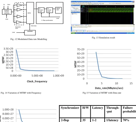
Mean time between failures of synchronizer depends on the data rate of asynchronous input metastability window, and frequency of receiving synchronizer. We are estimated the MTBF for varying the data rate, varying frequency, and metastability window and plotted on the graph shown in fig 14, 15, &16
5 Conclusions
Synchronizer circuit performance is characterised by MTBF .Non zero probability of failure exist for each synchronizer. MTBF is specified in 1028 years. As data rate is increased for the specified synchronizer, MTBF reduces drastically and failure probability increases. Similar is the case for metastability window and frequency of operation of synchronizer. Failure of synchronizer is sure if the data changes in the window .We have demonstrated the improved reliability of data synchronization by detecting data change in the window and provides alternative synchronizer which receives the delayed data for the same clock. The latency of the system is affected .Duplication of synchronizer is required .But it ensures correct data transfer.
Fig .12 Modulated Data rate Modelling Fig .13 Simulation result
Synchronizer H/W Latency Through-
-put
Failure probability
2-flop 35 1-2 1/latency 70%
Proposed scheme
100
0-1 1 10%
Fig .14 Variation of MTBF with Frequency Fig 15 Variation of MTBF with Data rate
6. References
[1] Ginosar Ran,“Metastability and synchronizer: A Tutorial”, IEEE Design &Test of computer,September/October 2011.
[2] Alshaikh M David Kiniment, Alex Yakovlev, “Robust Synchronization using wagging Technique”, Technical Report NCL-EECE – MSD-TR-2010 -165,University of Newcastle upon Tyne, 2010.
[3] Sohini Dasgupta , Alex Yakovlev , “Modelling and Performance analysis of GALS Architecture”, Technical Report NCL-EECE – MSD-TR-2006 -114,University of Newcastle upon Tyne, 2006.
[4] Ran Ginosar,and RKol, “Adaptive synchronisation”,1998 IEEE International Conference on Computer Design(ICCD’98),oct 1998. [5] David J kinniment,Charles E.Dike ,keith Heron,Gordon Russell, Alxander V Yakovlev, “Measuring Deep metastability and its effect
on synchronizer performance”,IEEE transaction on Very Large Scale Integration (VLSI) system, Vol 15,No-9 ,September 2007 . [6] Jun Zhou, David J kinniment,Charles E.Dike , Gordon Russell, Alxander V Yakovlev, “on chip measurement of Deep metastability
in synchronizer” IEEE Journal of Solid State Circuit,Vol 43,No-2 ,February-2008.
[7] Yaron Semiat and Ran Ginosar, “Timing Measurement of synchronization Circuit”, proceeding of Ninth International Symposium on asynchronous circuit and System,( ASYNC’2003).