Virginia Commonwealth University
VCU Scholars Compass
Theses and Dissertations Graduate School
2013
Performance and Reliability Study and Exploration
of NAND Flash-based Solid State Drives
Guanying Wu
Virginia Commonwealth University
Follow this and additional works at:http://scholarscompass.vcu.edu/etd
Part of theEngineering Commons © The Author
This Dissertation is brought to you for free and open access by the Graduate School at VCU Scholars Compass. It has been accepted for inclusion in Theses and Dissertations by an authorized administrator of VCU Scholars Compass. For more information, please [email protected].
Downloaded from
c
by Guanying Wu, 2013 All Rights Reserved.
Performance and Reliability Study and
Exploration of NAND Flash-based Solid State
Drives
A dissertation submitted in partial fulfillment of the requirements for the
degree of Doctor of Philosophy at Virginia Commonwealth University.
by
Guanying Wu
B. S., Zhejiang University, Hangzhou, China. July, 2007.
M. S., Tennessee Technological University, Cookeville, TN, USA.
December, 2009.
Director: Dr. Xubin He, Associate Professor
Department of Electrical and Computer Engineering
Virginia Commonwealth University
Richmond, Virginia
Acknowledgements
I would like to express the deepest appreciation to my committee chair Dr. Xubin He,
for his constant support and guidance at VCU as well as TTU in these years. Thanks to
him, I was able to develop my knowledge and skills in my field of study. In particular, I
am grateful I had his support to pursue the research in Solid State Technologies, which is
interesting, promising, as well as challenging. I also would like to thank Dr. Preetam
Ghosh, Dr. Robert H. Klenke, Dr. Weijun Xiao, and Dr. Meng Yu for serving on
my advisory committee. They were very much kind and thoughtful to me. Meanwhile,
our research group, The Storage Technology and Architecture Research (STAR) Lab, has
provided a joyful and incentive environment, from which I have benefited significantly in
both my study and life.
I would like to say thank you to my parents. I had to sacrifice the time to be around
them in the past five years and I am wishing to make it up as soon as I can. I am especially
grateful to my wife, who had been patient with me in my most miserable days. You could
Contents
List of Tables viii
List of Figures ix
Abstract xii
1 Introduction 1
1.1 Background . . . 1
1.1.1 NAND Flash Memory . . . 2
1.1.2 NAND Flash Program/Erase Algorithm . . . 3
1.1.3 NAND Flash-based SSDs . . . 5
1.2 Related Work: SSD Performance and Reliability . . . 8
1.3 Problem Statement . . . 10
1.4 Research Approaches . . . 10
2 Exploiting Workload Dynamics to Improve SSD Read Latency via Differenti-ated Error Correction Codes 11 2.1 Introduction . . . 11
2.2.1 NAND Flash Error Rate . . . 13
2.2.2 Error Correction Code Schemes . . . 16
2.3 Analysis and Modeling . . . 17
2.3.1 Write Speed vs. Raw Reliability Trade-off . . . 17
2.3.2 Read Access Latency . . . 18
2.3.3 Server Workload Analysis . . . 20
2.4 Architecture and Design of DiffECC . . . 24
2.4.1 System Overview . . . 24
2.4.2 Differentiated ECC Schemes: Trading-off between Write Speed and Read Latency. . . 26
2.4.3 Buffer Queue Scheduling Policy . . . 28
2.5 Evaluation . . . 31
2.5.1 Simulation Methodology . . . 31
2.5.2 The Optimistic Case of DiffECC . . . 32
2.5.3 The Controlled Mode-switching of DiffECC . . . 33
2.6 Summary . . . 37
3 Reducing SSD Access Latency via NAND Flash Program and Erase Suspen-sion 38 3.1 Introduction . . . 38
3.2 Motivation. . . 39
3.2.1 A Simple Demonstration of Contention Effect. . . 39
3.2.2 Configurations and Workloads . . . 40
3.3 Design . . . 43
3.3.1 Erase Suspension and Resumption . . . 43
3.3.2 Program Suspension and Resumption . . . 45
3.4 Further Discussions . . . 49
3.4.1 Scheduling Policy . . . 49
3.4.2 Implementation Issues . . . 51
3.4.3 The Overhead on Power Consumption . . . 52
3.5 Evaluation . . . 52
3.5.1 Read Performance Gain . . . 52
3.5.2 Write Performance . . . 55
3.6 Summary . . . 60
4 Delta-FTL: Improving SSD Lifetime via Exploiting Content Locality 61 4.1 Introduction . . . 61
4.2 Related Work Exploiting the Content Locality . . . 62
4.3 Delta-FTL Design . . . 64
4.3.1 Dispatching Policy: Delta Encode? . . . 65
4.3.2 Write Buffer and Delta-encoding. . . 66
4.3.3 Flash Allocation . . . 71
4.3.4 Mapping Table . . . 72
4.3.5 Garbage Collection . . . 74
4.4 Discussion: SSD Lifetime Extension of∆FTL. . . 75
4.4.1 Foreground Page Writes . . . 76
4.4.3 Summary . . . 79
4.5 Performance Evaluation . . . 79
4.5.1 Simulation Tool and SSD Configurations . . . 80
4.5.2 Workloads . . . 80
4.5.3 Emulating the Content Locality . . . 81
4.5.4 Experimental Results . . . 82 4.6 Summary . . . 89 5 Conclusions 91 List of Publications 94 Bibliography 96 Vita 106
List of Tables
1.1 Values from [3] for a Samsung 4 GB Flash Module. . . 3
1.2 Overhead difference among full merge, partial merge and switch merge.N stands for the number of pages per block; Nc means the number of clean pages in the data block. . . 7
2.1 Disk Traces Information . . . 21
2.2 BCH Parameters for Each Mode . . . 26
2.3 Latency results for different modes . . . 27
2.4 The Baseline Results under 32 MB Buffer (inms) . . . 32
3.1 Flash Parameters . . . 41
3.2 Disk Traces Information . . . 41
3.3 Numerical Latency Values of FIFO (inms) . . . 42
4.1 Delta-encoding Latency . . . 68
4.2 List of Symbols . . . 69
4.3 Flash Access Latency . . . 69
List of Figures
1.1 NAND flash memory structure. . . 2
1.2 Control-gate voltage pulses in program-and-verify operation. . . 4
1.3 Control Logic Block [10] . . . 4
1.4 Typical SSD Architecture [60]. . . 5
2.1 Threshold voltage distribution model NAND flash memory (except the erase state). . . 14
2.2 Simulation of SER under two different program step voltage ∆Vpp and hence different NAND flash memory write speed. . . 18
2.3 Data and ECC storage in the flash page: single segment and single ECC vs. multiple segments and multiple ECC. . . 20
2.4 Read latency reduction: pipelining bus transfer and ECC decoding via page segmentation. . . 20
2.5 The CDF of idle slot time of six traces. . . 23
2.6 Proposed system structure. . . 24
2.7 SER for two different modes. . . 27
2.8 Overview of the I/O queuing system. . . 28
2.9 The read and write performance of the optimistic case: 100%N(vc) = 8 writes. . . 33
2.11 Percentage of writes in each mode. . . 36
2.12 Percentage of reads in each mode. . . 36
3.1 Timing diagram illustrating the read latency under the effect of chip
contention. . . 40
3.2 Read Latency Performance Comparison: FIFO, RPS, PER, and PE0.
Results normalized to FIFO. . . 42
3.3 Read Latency Performance Comparison: RPS, PER, PE0, and PES IPC (P/E
Suspension using IPC). Normalized to RPS. . . 53
3.4 Read Latency Performance Comparison: PE0 and PES IPC (P/E
Suspen-sion using IPC). Normalized to PE0. . . 54
3.5 Read Latency Performance Comparison: PES IPC vs. PES IPS.
Normal-ized to PES IPC. . . 55
3.6 Write Latency Performance Comparison: FIFO, RPS, PES IPC, and
PES IPS. Normalized to FIFO. . . 56
3.7 Compare the original write latency with the effective write latency resulted
from P/E Suspension. Y axis represents the percentage of increased latency
caused by P/E suspension. . . 57
3.8 The percentage of writes that have ever been suspended. . . 58
3.9 The write latency performance of RPS and PES IPC while the maximum
write queue size varies. Normalized to FIFO. . . 59
3.10 Write Latency Performance Comparison: FIFO and PES IPC with
Write-Suspend-Erase enabled. Normalized to FIFO. . . 59
4.2 ∆FTL Temp Buffer . . . 67
4.3 ∆FTL Delta-encoding Timeline . . . 70
4.4 ∆FTL Mapping Entry. . . 72
4.5 ∆FTL Buffered Mapping Entry . . . 74
4.6 Normalized GC #: comparing baseline and∆FTL; smaller # implies longer SSD lifetime. . . 83
4.7 Normalized foreground write #: comparing baseline and∆FTL; smaller # implies: a) largerPcand b) lower consumption speed of clean flash space. . 84
4.8 Ratio of DLA writes (Pc). . . 84
4.9 Average GC gain (number of invalid pages reclaimed): comparing baseline and∆FTL; smaller # implies lower GC efficiency on reclaiming flash space. 85 4.10 Normalized average GC gain (number of invalid pages reclaimed): com-paring baseline and∆FTL. . . 86
4.11 Ratio of GC executed in DLA. . . 87
4.12 Normalized write latency performance: comparing baseline and∆FTL. . . 87
4.13 Normalized average GC overhead. . . 88
Abstract
PERFORMANCE AND RELIABILITY STUDY AND EXPLORATION OF NAND
FLASH-BASED SOLID STATE DRIVES
By Guanying Wu
A Dissertation submitted in partial fulfillment of the requirements for the degree of Doctor
of Philosophy at Virginia Commonwealth University.
Virginia Commonwealth University, 2013
Major Director: Dr. Xubin He, Associate Professor, Department of Electrical and
Computer Engineering
The research that stems from my doctoral dissertation focuses on addressing essential
challenges in developing techniques that utilize solid-state memory technologies (with
em-phasis on NAND flash memory) from device, circuit, architecture, and system perspectives
in order to exploit their true potential for improving I/O performance in high-performance
computing systems. These challenges include not only the performance quirks arising from
read/write performance asymmetry, and slow and constrained erase functionality, but also
the reliability drawbacks that limits solid state drives (SSDs) from widely deployed.
To address these challenges, I have proposed, analyzed, and evaluated the I/O
schedul-ing schemes, strategies for storage space virtualization, and data protection methods, to
boost the performance and reliability of SSDs.
Key Words: Solid state devices; NAND flash memory; Data Storage; Performance;
Chapter 1
Introduction
Solid State Drives (SSD’s) have shown promise to be a candidate to replace traditional
hard disk drives. The benefits of SSD’s over HDD’s include better durability, higher
performance, and lower power consumption, but due to certain physical characteristics
of NAND flash, which comprise SSDs, there are some challenging areas of improvement
and further research. In this section, I will begin with an introduction to the subject of my
research, i.e., NAND flash memory and SSDs, followed by a statement of key problems to
address as well as a summary of proposed approaches.
1.1
Background
In this section, I will briefly overview the related background of my research, i.e.,
1.1.1
NAND Flash Memory
In general, the data retention of NAND flash memory is done by the charge trapped in
the floating gate of the flash cell, and the amount of charge determines the logical level
of a certain cell. According to the maximum number of levels defined when the data are
retrieved, there are two primary types of NAND flash memory: Single-level cell (SLC)
and Multi-level cell (MLC). As one would expect, single-level cell flash stores one bit per
transistor, while multi-level cell flash stores multiple bits per transistor. MLC is one of the
efforts made for increasing the storage density of the flash.
Bit-line Bit-line
Source line Word-line
Word-line Word-line Select gate line
Select gate line
Bit-line
Cell String
Page buffer
One or more pages
Figure 1.1: NAND flash memory structure.
To further push the storage density envelope, NAND flash memory cells are organized
in an array→page→block hierarchy (Figure 1.1), where a NAND flash memory array is partitioned into blocks, and each block contains a number of pages. Within each block,
each memory cell string typically contains 64 to 256 memory cells, and all the memory
cells driven by the same word-line are programmed and sensed at the same time. All the
and fetched in the unit of page. The read operation consists of sensing and loading the data
from cells to the page buffer and transmitting the data from page buffer to a flash controller.
The write operation consists of receiving the data page to be written from the flash
controller, loading the page buffer with the data, and then writing on the flash page using
ISPP (Incremental Step Pulse Program [10]). The erase operation simply takes a long erase
pulse (in micro seconds) to reset the cells in the target flash block. Typical access latency
values of these operations are listed in Table1.1.
Table 1.1: Values from [3] for a Samsung 4 GB Flash Module.
Page Read to Register 25µs
Page Program from Register 200µs
Block Erase 1.5 ms
1.1.2
NAND Flash Program/Erase Algorithm
Compared to the read operation which simply applies the predefined voltage bias on the cell
and detects whether the cell is turned on or not, the P/E operations are more complex in that
the charging/discharging process should be precisely controlled to achieve a pre-defined
amount of charges in the cells [8]. One state-of-the-art technique known as “Incremental
Step Pulse Program”(ISPP) is used for the flash programming [10]. It consists of a series
of program and verify iterations. For each iteration, the program pulse voltage, Vpp, is
increased by ∆Vpp, which is normally a few tenth of a volt [77]. ISPP is illustrated in
Fig.1.2. For the erase operation, the duration of the discharge/erase voltage applied on the
flash cells is ensured to remove the charges in all cells of one flash block. Therefore, the
P/E latency of NAND flash is much higher than the read latency. The execution of ISPP and
pp pp
Figure 1.2: Control-gate voltage pulses in program-and-verify operation.
block. The analog block is responsible for regulating and pumping the voltage for program
or erase operations. The control logic block is responsible for interpreting the interface
commands, generating the control signals for the flash cell array and the analog block,
and executing the program and erase algorithms. As shown in Figure 1.3, the write state
machine consists of three components: an algorithm controller to execute the algorithms
for the two types of operations, several counters to keep track of the number of ISPP
iterations, and a status register to record the results from the verify operation. Both
Algorithm Controller Counters Status Register Command Interface Write State Machine
Requests
To Analog Block and Flash Array
From Flash Array
Figure 1.3: Control Logic Block [10]
program and erase operations require a precise timing control, i.e., the program or erase
voltage pulse that applies on the cell must be maintained for the predefined time period,
1.1.3
NAND Flash-based SSDs
Figure 1.4: Typical SSD Architecture [60].
The NAND flash by itself exhibits relatively poor performance [78, 75]. The high
performance of an SSD comes from leveraging a hierarchy of parallelism. At the lowest
level is the page, which is the basic unit of I/O read and write requests in SSDs. Erase
operations operate at the block level, which are sequential groups of pages. A typical
value for the size of a block is 64 to 256 pages. Further up the hierarchy is the plane,
and on a single die there could be several planes. Planes operate semi-independently,
offering potential speed-ups if data is striped across several planes. Additionally, certain
copy operations can operate between planes without crossing the I/O pins. An upper
level of abstraction, the chip interfaces, free the SSD controller from the analog processes
of the basic operations, i.e., read, program, and erase, with a set of defined commands.
NAND interface standards includes ONFI [56], BA-NAND [56], OneNAND [62],
LBA-NAND [71], etc. Each chip is connected via the data buses to the central control unit of
an SSD, which is typically implemented in one micro-processor coupled with RAMs. The
SSDs hides the underlying details of the chip interfaces and exports the storage space
as a standard block-level disk via a software layer called Flash Translation Layer (FTL),
running on the in-drive micro-processor. The typical SSD architecture is illustrated in
Figure1.4 [60]. FTL is a key component of an SSD in that it not only is responsible for
managing the “logical to physical” address mapping but also works as a flash memory
allocator, wear-leveler, and garbage collection engine.
Mapping Schemes
The mapping schemes of FTL’s can be classified into two types: page-level mapping, with
which a logical page can be placed onto any physical page; or block-level mapping, with
which the logical page LBA is translated to a physical block address and the offset of
that page in the block. Since with block-level mapping, one logical block corresponds
to one physical block, we refer a logical block on a physical block as a data block. As
the most commonly used mapping scheme, Log-block FTL’s [61] reserve a number of
physical blocks that are not externally visible for logging pages of updated data. In
log-block FTL’s, log-block-level mapping is used for the data log-blocks, while page-level mapping
is for the log blocks. According to the block association policy (how many data blocks
can share a log block), there are mainly three schemes,block-associative sector translation
(BAST) [38], fully-associative sector translation (FAST) [41], and set-associative sector
translation (SAST) [32]. In BAST, a log block is assigned exclusively to one data block;
in FAST, a log block can be shared among several data blocks; SAST assigns a set of data
Garbage Collection Process
In the context of log-block FTL’s, when free log blocks are not sufficient, the garbage
collectionprocess is executed, which merges clean pages on both the log block and data
block together to form a data block full of clean pages. Normally this process involves the
following routine: read clean pages from the log block and the corresponding data block(s)
and form a data block in the buffer; erase the data block(s) and log block; program the data
on a clean physical block (block that contains no data at all). Sometimes the process can be
quite simplified: if we consider a log block that contains all the clean pages of an old data
block, the log block can just replace the old data block; the old data block can be erased,
making one clean physical block. We refer to the normal process as full merge and the
simplified one asswitch merge. APartial mergehappens when the log block contains only
(but not all) clean pages of one data block, and the garbage collection process only requires
that the rest of the clean pages get copied from the data block to the log block. Afterwards,
the log block is then marked as the new data block and the old data block gets erased.
To make a quantitative view of the overhead of different merge routines, Table 1.2
compares the numbers of clean page reading, page programming, and block erase, which
are involved in garbage collection routine of the BAST FTL. The former two are in the
order of number of pages, and the last one is in number of blocks.
Table 1.2: Overhead difference among full merge, partial merge and switch merge. N
stands for the number of pages per block;Ncmeans the number of clean pages in the data
block.
Full merge Partial merge Switch merge
Clean page reading N Nc 0
Page programming N Nc 0
1.2
Related Work: SSD Performance and Reliability
To improve the performance and reliability of flash-based SSDs, many designs have been
proposed in the literature working with the file system, FTL, cache scheme, etc.
File systems: Early flash file systems such as YAFFS [52] and JFFS2 [25] are designed
for embedded systems and work on the raw flash. On the contrary, DFS [30] is implemented
over the virtualized flash interface offered by Fusion-IO driver. By leveraging this interface,
it avoids the complexity of physical block management of traditional file systems.
FTLs: For block-level mapping, several FTL schemes have been proposed to use a
number of physical blocks to log the updates. Examples include FAST [41], BAST [38],
SAST [32], and LAST [43]. The garbage collection of these schemes involves three
types of merge operations, full, partial, andswitchmerge. The block-level mapping FTL
schemes leverage the spacial or temporal locality in write workloads to reduce the overhead
introduced in the merge operations. For page level mapping, DFTL [23] is proposed
to cache the frequently used mapping table in the in-disk SRAM so as to improve the
address translation performance as well as reduce the mapping table updates in the flash;µ
-FTL [44] adopts theµ-tree on the mapping table to reduce the memory footprint. Two-level
FTL [73] is proposed to dynamically switch between page-level and block-level mapping.
Content-aware FTLs (CAFTL) [15][22] implement the deduplication technique as FTL in
SSDs. ∆FTL [74] exploits another dimension of locality, the content locality, to improve
the lifetime of SSDs.
Cache schemes: A few in-disk cache schemes like BPLRU [37], FAB [29], and
BPAC [76] are proposed to improve the sequentiality of the write workload sent to the
as an OS level scheduling policy, chooses to prioritize the clean cache elements when doing
replacements so that the write commitments can be reduced or avoided. Taking advantage
of fast sequential performance of HDDs, Griffin [66] and I-CASH [79] are proposed to
extend the SSD lifetime by caching SSDs with HDDs. FlashTier [63] describes a system
architecture built upon flash-based cache geared with dedicated interface for caching.
Heterogeneous material: Utilizing advantages of PCRAM, such as the in-place update
ability and faster access, Sunet al.[69] describe a hybrid architecture to log the updates on
PCRAM for flash. FlexFS [42], on the other hand, combines MLC and SLC as trading off
the capacity and erase cycle.
Wear-leveling Techniques: Dynamic wear-leveling techniques, such as [65], try to
recycle blocks of small erase counts. To address the problem of blocks containing cold
data, static wear-leveling techniques [14] try to evenly distribute the wear over the entire
SSD.
Read/Write Speed vs. Reliability Trade-offs: NAND flash memory manufacturers must
reserve enough redundant bits in the flash pages to ensure the worst case reliability at the
end of their lifetime. Y. Pan et al. proposed to trade the such reliability over-provisioning
(at the early age of the flash memory) for faster write speed by increasing∆Vpp [58]. S.
Lee et al. proposed to exploit the self-recovery mechanics of NAND flash memory to
dynamically throttle the write performance so as to prolong the SSD lifetime [40]. In [47]
R. Liu et al. proposed to trade the retention time of NAND flash for faster write or shorter
1.3
Problem Statement
SSD Read Performance Issues: The read access latency is a critical metric of SSDs’
performance, attributed to 1) raw access time including on-chip NAND flash memory
sensing latency, flash-to-controller data transfer latency, and ECC decoding latency; 2)
the queuing delay.
SSD Reliability Issues: The limited lifetime of SSDs is a major drawback that
hinders their deployment in reliability sensitive environments. Pointed out in the literature,
“endurance and retention of SSDs is not yet proven in the field” and “integrating SSDs into
commercial systems is painfully slow”. The reliability problem of SSDs mainly comes
from the following facts. Flash memory must be erased before it can be written and it may
only be programmed/erased for a limited times (5K to 100K) [21]. In addition, the
out-of-place writes result in invalid pages to be discarded by garbage collection (GC). Extra
writes are introduced in GC operations to move valid pages to a clean block [3] which
further aggravates the lifetime problem of SSDs.
1.4
Research Approaches
On the SSD read performance issues, two approaches (DiffECC discussed in Chapter2and
Program/Erase Suspension discussed in Chapter3) are proposed to reduce the latency from
two perspectives, i.e., the raw read latency and queuing delay, respectively. To enhance
SSD reliability, my work (Delta-FTL discussed in Chapter 4 falls into the area of FTL
design. Delta-FTL leverages the content locality to prolong SSD lifetime via the idea of
Chapter 2
Exploiting Workload Dynamics to
Improve SSD Read Latency via
Differentiated Error Correction Codes
2.1
Introduction
As pointed out in [39], the read access latency is another critical metric of SSDs. SSD
read access latency mainly consists of on-chip NAND flash memory sensing latency,
flash-to-controller data transfer latency, and ECC (Error Correction Code) decoding latency.
There is an inherent trade-off between storage density and read access latency. The storage
density can be improved by using a larger NAND flash page size. Moreover, if each entire
page is protected by a single ECC, the coding redundancy can be minimized, leading to
codeword inevitably increases the read access latency, in particular the flash-to-controller
data transfer latency and ECC decoding latency.
This work presents a cross-layer design strategy that can reduce the average SSD read
access latency when large NAND flash memory page size is used. This design strategy
is motivated by an inherent NAND flash memory device write speed vs. raw storage
reliability trade-off: if we can intentionally slow down NAND flash memory internal write
operation, which can enable a finer-grained control of memory cell programming states,
the raw NAND flash memory storage reliability will accordingly improve. Therefore,
by leveraging run-time workload variability, if the SSD controller can opportunistically
slow down the NAND flash memory write operation through appropriate use of data
buffering, it can opportunistically use different ECC coding schemes to reduce the read
access latency. In particular, if NAND flash memory is allowed to write one page of data
with a slower-than-normal speed and hence better-than-normal raw storage reliability, this
page can be partitioned into several segments and each segment is protected by a shorter
and weaker ECC. As a result, when this page is being read, since each small segment
can be decoded independently, the flash-to-controller data transfer and ECC decoding can
be largely overlapped, leading to a dramatically reduced flash read latency. The data
access workload variation naturally allows us to take advantage of the bandwidth at the
idle time to slow down the write speed of the SSDs in order to opportunistically improve
SSD read response speed, as discussed above. In this work, we propose a disk level
scheduling method to smooth the write workload and opportunistically slow down certain
write operations.
It should be pointed out that this proposed design approach does not sacrifice the SSD
flash memory device write operations when the device is idle, because of the data access
workload variation in the run time. Moreover, for writes, the OS page cache works on
scheduling the actual commitment on the disks and hiding the write latency. With the
aid of on-disk write buffer, the disk can adopt thewrite-back scheme which reports write
completion as soon as the data are buffered. These factors can be naturally leveraged to
improve the probability of opportunistic write slow down.
In the rest of this chapter,DiffECC, a novel cross-layer co-design to improve SSD read
performance using differentiated ECC schemes, is proposed, discussed, and evaluated in
detail.
2.2
Background
In this section, a model of bit error rate of NAND flash memory is introduced, followed by
a brief discussion about the error correction coding schemes (with emphasis on BCH code)
used to protect NAND flash from bit errors.
2.2.1
NAND Flash Error Rate
Ideally, threshold voltage distributions of different storage states should be sufficiently far
away from each other to ensure a high raw storage reliability. In practice, due to various
affects such as background pattern dependency, noises, and cell-to-cell interference [18],
the threshold voltage distributions may be very close to each other or even overlap, leading
to non-negligible raw bit error rates. In the following, we present an MLC cell threshold
voltage distribution model that will be used for quantitative performance evaluation and
[70], i.e., the probability density function (PDF) of the threshold voltage distribution can be approximated as p0(x) = 1 σ0 √ 2π ·e −(x−µ)2 2σ20
whereσ0 is the standard deviation andµis the mean threshold voltage of the erase state.
All the other states tend to have the same threshold voltage distribution, as illustrated
in Fig. 2.1. The model consists of two parts, an uniform distribution in the middle and
Gaussian distribution tail on both sides [70]. The width of the uniform distribution equals
Vpp
Figure 2.1: Threshold voltage distribution model NAND flash memory (except the erase state).
to the program step voltage∆Vpp, and the standard deviation of the Gaussian distribution
is denoted as σ. The Gaussian distribution on both sides models the overall effect of
background pattern dependency, noises, and cell-to-cell interference. LetP0 andP1denote
have the overall PDFfpr(x)as fpr(x) = c σ√2π, b−0.5∆Vpp ≤x≤b+ 0.5∆Vpp c σ√2πe −(x−b−0.5∆Vpp)2 2σ2 , x > b+ 0.5∆Vpp c σ√2πe −(x−b+0.5∆Vpp)2 2σ2 , x < b−0.5∆Vpp
whereb is the mean of the threshold voltage (i.e., the center of the distribution as shown
in Fig.2.1), and the constantccan be solved based on P0 +P1 =
R+∞
−∞ fpr(x)dx = 1. It
is clear that, as we reduce the program step voltage ∆Vpp, adjacent states will have less
probability to overlap. Hence the raw storage reliability will improve, while the memory
write latency will accordingly increase. This suggests that there is an inherent trade-off
between NAND flash memory write latency and raw storage reliability.
The use of a larger page size can increase the effective NAND flash memory storage
density from two perspectives: (i) A larger page size enables more memory cells share the
same word-line, leading to a more compact memory cell array layout and hence higher
storage density; (ii) Given the same raw bit error rate, ECC with a longer codeword tends
to use less coding redundancy (i.e., higher code rate). A larger page size enables the use
of ECC with longer codeword length, leading to less coding redundancy and hence higher
effective storage density. However, a large page size apparently will result in a longer time
to transmit the data from the flash die to the controller. Meanwhile, the ECC decoding
latency may increase as the codeword length increases. As a result, the read response time
2.2.2
Error Correction Code Schemes
As the storage density continues to grow, NAND flash memory uses increasingly powerful
ECC on each individual page to ensure storage reliability [8]. A more powerful ECC
with stronger error correction capabilities, tends to demand more redundant bits, which
causes an increase in requirements for storage space. Therefore, designers always select
an ECC that provides just enough error correction capability to satisfy the given reliability
specifications. Moreover,with the same code rate, the longer the codeword is, the better
the coding efficiency is. Hence, as pointed out earlier, ECC with a longer codeword length
requires less coding redundancy and thus leads to a higher storage density. In current design
practice, binary BCH code is being widely used in NAND flash memories [20][17][68].
Binary BCH code construction and encoding/decoding are based on binary Galois
Fields [46]. A binary Galois Filed with degree of m is represented as GF(2m). For any
m ≥ 3and and t < 2m−1, there exists a primitive binary BCH code over GF(2m), which has the codeword length n = 2m − 1 and information bit length k ≥ 2m − m ·t and can correct up to (or slightly more than) t errors. A primitivet-error-correcting (n, k, t)
BCH code can be shortened (i.e., eliminate a certain number, say s, of information bits)
to construct at-error-correcting (n−s, k−s, t) BCH code with less information bits and code length but the same redundancy. Given the raw bit error ratepraw, an (n, k, t) binary
BCH code can achieve a codeword error rate of
Pe = n X i=t+1 n m piraw(1−piraw)n−i
Binary BCH encoding can be realized efficiently using linear shift registers, while binary
to t2. Readers can refer to [9] and [46] for a more detailed discussion of various BCH
decoding algorithms.
2.3
Analysis and Modeling
In this section, we first demonstrate how write speed would affect the raw reliability by
an example; then we discuss about reducing the read latency via page segmentation and
weaker/shorter ECC; finally, we explore the potential of applying the differentiated ECC
scheme through an analysis of read-world disk I/O workloads.
2.3.1
Write Speed vs. Raw Reliability Trade-off
A slowing down write speed which is reflected by a smaller program step voltage∆Vppcan
improve the raw NAND flash memory reliability due to the narrowedVthdistribution. Let
us consider 2bits/cell NAND flash memory as an example. We set the program step voltage
∆Vppto 0.4 as a baseline configuration and normalize the distance between the mean of two
adjacent threshold voltage windows as 1. Given the value of program step voltage∆Vpp,
the BCH code decoding failure rate (i.e., the page error rate) will depend on the standard
deviations of the erased state (i.e.,σ0) and the other three programmed states (i.e., σ). We
fix the normalized value ofσ0 as 0.1 and carry out simulations to evaluate the sector error
rate vs. normalizedσ, as shown in Fig.2.2. The results clearly show that only 5% reduction
0.108 0.11 0.112 0.114 0.116 0.118 0.12 10−15 10−10 10−5 100 σ
Sector Error Rate (SER)
BCH(34528, 32800, 108), ΔV
pp=0.400(100%) BCH(34528, 32800, 108), ΔV
pp=0.380(95%)
Figure 2.2: Simulation of SER under two different program step voltage∆Vppand hence
different NAND flash memory write speed.
2.3.2
Read Access Latency
Read access latency includes the on-chip NAND flash sensing latency, flash-to-controller
data transfer latency, and ECC decoding latency. The on-chip NAND flash sensing latency
is typically a few tens of µs. Assuming the NAND flash chip connects with the SSD
controller through a 100MHz 8-bit I/O bus, it takes at least 40.96µs and 20.48µs to transfer
one page from NAND flash chip to controller when the page size is 4 KB and 2 KB,
respectively. Typically,ECC decoding delay is linearly proportional to its codeword length.
Hence, the use of large page size will inevitably result in a longer ECC decoding delay. For
example, assuming the use of parallel BCH code decoder architecture presented in [68],
we estimate that the overall BCH decoding latency is 41.2µs and 22.3µs when using one
BCH code to protect 4 KB and 2 KB user data, respectively. Therefore, if we assume
the on-chip NAND flash page sensing latency is 25µs, the overall read access latency is
107.16µs and 67.78µs when the page size is 4 KB and 2 KB, respectively. It suggests that
4 KB. As pointed out earlier, the use of large page size is beneficial from storage density
perspective. To improve the read response time while increasing page size, straightforward
solutions include the use of higher speed I/O bus and/or higher throughput BCH decoder.
However, increasing the bus speed and/or decoder throughput will greatly increase the
power consumption and silicon cost.
NAND flash memory has an inherent write speed vs. raw storage reliability trade-off.
Therefore, if we could exploit the run-time workload variability and use the on-chip buffer
in SSD controller to opportunistically slow down the NAND flash write operations, we can
opportunistically increase the NAND flash raw storage reliability and hence use shorter and
weaker ECC, which can directly reduce overall read access latency. This intuition leads to
the basic idea of this work, i.e., by opportunistically slowing down NAND flash memory
write operations, we can use different ECC coding schemes in order to reduce average
overall SSD read access latency.
In particular, given better NAND flash memory raw storage reliability from slow
programming speed, we can partition one large page into a few smaller segments, each
one is protected with one shorter (thus weaker) ECC. Figure2.3(a) illustrates the baseline
mode of data and ECC storage in the flash page where the entire data area is encoded with
ECC as a whole; Figure2.3(b) shows an example of the proposed page segmentation: the
data is split into 4 segments and each segment is encoded with ECC individually.
With segmentation, the flash-to-controller data transfer and ECC decoding can be
largely overlapped, i.e., once the controller receives the first segment, it starts to decode
while the following segments are being transferred. This can largely reduce the overall
read access time of a flash page. We illustrate this idea in Figure 2.4: after the flash
Data ECC Other OOB Info
(a) Single segment, single ECC
(b) Multiple segments, multiple ECCs
Data Seg 1 ECC 1 Data Seg 2 ECC 2 Data Seg 3 ECC 3 Data Seg 4 ECC 4 Other OOB
Info
Figure 2.3: Data and ECC storage in the flash page: single segment and single ECC vs. multiple segments and multiple ECC.
and ECC decoding period (Tecc decode) without being able to overlap these two periods.
However, with segmentation, because Tbus of current segment transfer and Tecc decode of
previous segment decoding are independent of each other and thus can be overlapped, we
may achieve reduced read latency compared to the baseline mode.
(a) Single segment, single ECC
(b) Multiple segments, multiple ECCs Tecc_decode Tread_raw Tbus
Tbus Tecc_decode
Tbus Tecc_decode
Tbus Tecc_decode
Tread_raw Tbus Tecc_decode
Figure 2.4: Read latency reduction: pipelining bus transfer and ECC decoding via page segmentation.
2.3.3
Server Workload Analysis
The workloads of the servers are often time-varying, while to build a server, the
hardware/software configurations are determined by the needs of the peak performance,
which is often affected by the request burstness. For example, Kavalanekar et al. [35]
Table 2.1: Disk Traces Information Parameter F1 F2 C3 C8 DAP MSN Reads(106) 1.23 3.04 0.75 0.56 0.61 0.40 Read % 23.1 82.3 35.3 27.4 56.2 75.0 Compression Ratio X10 X30 X3 X3 X8 X50 ARR 1240 3223 576 666 135 1245 Idle % 52.2 51.6 57.4 56.0 63.9 66.2 W Rmax% 93.8 73.0 91.5 97.3 99.2 45.6
that most of them show a high level of burstiness, which is measured in self-similarity.
Self-similarity means bursts occur at a wide range of time scales, e.g., the diurnal pattern
is a day-scale factor; the Internet traffic, which incurs congestions, is a minute-scale factor;
the operating system, which periodically flush the dirty data, is a millisecond to second
scale factor. In addition, the I/O behavior of the application contributes to the variations
at various time scales. Meeting the peak performance needs makes the bandwidth of
the hardwares under fully-exploited, especially for the self-similar workloads which have
concentrated bursts.
To learn about the workload stress on the SSDs, we have conducted trace-driven
simulation experiments with an SSD simulator based on the Microsoft Research SSD
extension [3] for Disksim 4.0. The simulated SSD is configured realistically to match a
typical SSD: there are 16 flash chips, each of which owns a dedicated channel to the flash
controller. Each chip has four planes that are organized in a RAID-0 fashion; the size of one
plane is 1 GB assuming the flash is used as 2-bit MLC (page size is 4 KB). To maximize the
concurrency, each individual plane has its own allocation pool [3]. The garbage collection
processes are executed in the background so as to minimizing the interference upon the
foreground requests. In addition, the percentage of flash space overprovisioning is set as
30%, which doubles the value suggested in [3]. Considering the limited working-set size
avoid garbage collection processes to be executed too frequently. The garbage collection
threshold is set as 10%, which means if the clean space goes below 10% of the exported
space, the garbage collection processes are triggered. Here we only report the results with
buffer size of 64 MB. The SSD is connected to the host via PCI-E of 2.0 GB/s.
We played back a few real-world disk I/O traces in our simulation experiments.
Financial 1 andFinancial 2(F1, F2) [67] were obtained from OLTP applications running
at two large financial institutions; the Display Ads Platform and payload servers(DAP)
andMSN storage metadata(MSN) traces were from the Production Windows Servers and
described in [35](note that we only extracted the trace entries of the first disk of
MSN-CFS); the Cello99 [27] trace pool is collected from the “Cello” server that runs HP-UX
10.20. Because the entireCello99is huge, we randomly use one day traces (07/17/99) of
two disks (C3 and C8). These disk I/O traces are originally collected on HDD systems.
To produce more stressful workloads for SSDs, we deliberately compressed the simulated
time of these traces so that the system idle time is reduced from originally 98% to about
50∼60%. Some basic information of these traces can be found in Table2.1, where “ARR” stands for average request rate(requests per second); “compression ratio” means the ratio
of simulation time compression done for each traces.
There are a few applications that take advantage of the idle slots, such as disk
scrubbing [57], system checkpointing, data backup/mining, etc., which normally run
between the midnight to daybreak. Our design differs from these applications in that it
works on a smaller time scale, in particular we buffer the writes and dispatch them over
the idle slots between foreground requests. With the original traces, we collected the idle
slot time CDF in Figure2.5. Except for DAP, the rest traces all have over 40% of idle slots
< 5 < 10 < 15 < 20 < 25 < 30 < 40 < 50 < 60 60+ 0 0.1 0.2 0.3 0.4 0.5 0.6 0.7 0.8 0.9 1 Idle Time (ms) CDF F1 F2 C3 C8 DAP MSN
Figure 2.5: The CDF of idle slot time of six traces.
few milliseconds, SSDs can do dozens of page writes or hundreds of pages reads with the
bandwidth of a single flash chip. Or we can buffer writes and slowly program them with
weak ECC in the idle slots, then while read accesses occur on those pages, we may have a
reduced read latency.
So, what is the chance of reading a weak ECC coded page? Ideally, assuming all
page writes could be programmed slowly and coded with weak ECC, the chance is then
determined by the overlap of the working-sets of reads and writes. We simulated this case
with the above six traces, assuming the data are initially programmed in strong ECC. The
percentage of weak ECC reads is denoted asW Rmaxin Table2.1. For the listed six traces,
W Rmaxranges from 45.6% to 99.2%, suggesting a promising potential gain on read latency
2.4
Architecture and Design of DiffECC
In this section, we first outline the architecture of our proposed design and then depict
its major components including the differentiated ECC schemes and the write request
scheduling policy in detail.
2.4.1
System Overview
Write Buffer Adaptive BCH
encoder Flash die
Adaptive BCH decoder
Write Speed
Write Latency Controller
Figure 2.6: Proposed system structure.
Fig.2.6shows the system structure of the proposed design approach. In order to smooth
the workload, an on-disk write buffer with capacity m is managed by our I/O scheduling
policy. We dynamically adjust the code length of BCH encode/decoder and the write speed,
according to the scheduling policy. The adaptive BCH encoder will accordingly partition
the page of length L intoN(vc) segments and encode each segment with BCH codes at
length ofL/N(vc). N(vc) = 1represents no partition is performed and the system writes
at full speed. We further make the following assumptions: the data on the SSD programmed
at the speed ofvcare read with the probability ofα(vc); the decoding latency of the BCH
decoder at length of L/N(vc) is Tdec(vc); the bus transfer time is slightly less than ECC
decoding time (as illustrated in Figure2.4); and the average number of requested segments
on the target page isn(vc)(n(vc)<=N(vc)). We can estimate the average read latency as:
Tread raw+ X vc α(vc)( Tbus N(vc) +Tdec(vc)∗n(vc)) (2.1)
whereTbusis the bus delay when the whole page is transmitted through the bus from the
NAND flash chip to the controller, andTread rawis the delay when the data are sensed from
the cells and transferred to the page buffer. We also note that, since this design strategy is
applied to each page independently, it is completely transparent to the operating systems
and users. Pointed out in Section2.4 that ECC decoding delay is linearly proportional to
its codeword length. Thus, Tdec(vc) in Expression2.1 is approximately the value of ECC
decoding time of the baseline mode (no segmentation and strong ECC) devided byN(vc).
The analytical modeling for the expected read performance discussed above is
straight-forward. However, the actual performance under real-world workloads is difficult to
estimate, due to a few reasons. First, as we discussed in Section2.3, theα(vc)is workload
specific. Second, although doing 100% slow writes does not involve in much overhead
with the HDD traces, in practice, heavier workload may be expected. So we can not
always assume a 100% slow write. Third, bursts come in the term of high request rate
or batched requests, which are often queued. With a queuing system, Equation 2.1 only
outlines the physical access latency improvement of the reads. For example, if there are
many writes ahead of a read, the long queuing time would trivialize the latency reduction
resulted from weak ECC, especially, for the “Read After Write” access pattern, the read has
to be arranged after the write if no cache exists. The slow writes may additionally increase
2.4.2
Differentiated ECC Schemes: Trading-off between Write Speed
and Read Latency
In order to achieve the best possible performance, N(vc) should be able to vary within a
large range and accordingly ECCs with many different code lengths should be supported
by the controller. However, such an ideal case may incur prohibitive amount of
implementation complexity and hence may not be practicable. In this work, to minimize
the implementation overhead, we set that the system can only switch between four modes,
a normal mode (also used as the baseline mode) and three slow write modes. For the
baseline normal mode, we set N(vc) = 1 and use a (34528, 32800, 108) BCH code in
order to minimize the coding redundancy. For the slow write modes, we setN(vc)as 2, 4,
and 8, considering the trade-off between required write speed slow down and read response
latency improvement. The BCH coding parameters of each modes are listed in Table2.2.
Table 2.2: BCH Parameters for Each Mode
N(vc) Segment Size BCH(n,k,t)
1 4KB (34528, 32800, 108)
2 2KB (17264, 16400, 57)
4 1KB (8632, 8200, 30)
8 512B (4316, 4100, 16)
We assume the use of 2 bits/cell NAND flash memory. We set the program step voltage
∆Vppto 0.4 and normalize the distance between the mean of two adjacent threshold voltage
windows as 1. Given the value of program step voltage ∆Vpp, the sector error rate (SER)
will depend on the standard deviations of the erased state (i.e., σ0) and the other three
programmed states (i.e., σ). In the following simulation, we fix the normalized value of
σ0 as 0.1 and evaluate the SER vs. normalized σ. For the slow write modes, under the
sameσ0, we run the exhaustive simulation to choose a just slow enough∆Vppto ensure the
we demonstrate the derivation of∆Vpp of modeN(vc) = 8as an example in Fig.2.7. We
can observe that ∆Vpp =0.265 (66.25% of the baseline, corresponding to a write latency
overhead of 50.9%) is just able to compensate the performance loss caused by the using of
short BCH code (4316, 4100, 16) instead of the (34528, 32800, 108) BCH code.
0.108 0.11 0.112 0.114 0.116 0.118 0.12 10−15 10−10 10−5 100 σ
Sector Error Rate (SER)
BCH(34528, 32800, 108), ΔVpp=0.400(100%) BCH(4316, 4100, 16), ΔVpp=0.265(66.25%)
Figure 2.7: SER for two different modes.
Targeting at the throughput of 3.2Gbps and based on the hardware structure of [68],
we further carry out the ASIC design of BCH decoders for the above BCH codes. TSMC
65nm standard CMOS cell and SRAM libraries are used in the estimation. We summarize
the BCH decoding latency values of the four modes (as well as the write latency, bus
transfer latency, etc.) in Table2.3. This work assumes 25µs of cell to buffer read latency
(Tread raw) and 100 MB/s bus bandwidth.
Table 2.3: Latency results for different modes
N(vc) Write Latency(µs)
Read Latency (µs)
BCH Bus Cell to buffer Total
1 500 41.20 40.96 25 107.16
2 538 21.71 20.48 25 67.19
4 606 11.25 10.24 25 46.49
I/O Queue
Host Interface Logic
FTL SRAM Buffer Flash Memory Host System SSD File System Buffer Cache I/O Driver Out Base Queue Priority Queue Differentiated Writes Writes Reads Evictions Reads
Figure 2.8: Overview of the I/O queuing system.
2.4.3
Buffer Queue Scheduling Policy
The goal of our scheduling policy is to take advantage of the idle time bandwidth of SSDs
so as to slow down the write speed. Intuitively, we choose to utilize the on-disk SRAM
cache to buffer the write requests, and synchronize them on the flash with high or low write
speed according to the on-line load of the SSD.
Typical SSDs are equipped with an SRAM buffer, which is responsible for
buffering/re-scheduling the write pages and temporally hold the read data which are to be passed on to
the OS. The size of the buffer normally ranges from 32 MB to 128 MB according to the
class of the product. Because of the fast random read speed of flash memory and the
relatively small size of the SRAM, the cache is dedicated to writes exclusively. The write
scheme of the buffer is set as “write-back”, which means completions are reported as soon
as the data are buffered. While accommodating the new data and buffer is out of space, the
replacements take place. The victim (dirty) pages are inserted into an I/O queue in which
buffer space of the victims is freed and can accept new data. In this way, the maximum
number of write pages holding in the queue is determined by the size of the buffer, e.g.,
with a 32 MB buffer, the number is 65536 assuming the sector size is 512B.
Given a workload, of what portion the writes can be done in slow modes? Ideally, taking
out the bandwidth the SSD spends on the reads, the slow and fast writes can share the rest.
For simplicity, let us assume there are two write modes in the following discussion, one
slow mode (N(vc) >1) and one normal mode (N(vc) = 1). The maximum throughput of
slow write is denoted asΘsrequests/s andΘnfor the normal write, and we haveΘs <Θn.
According to different average write request rates(ARRw), there are two scenarios.
• Case 1: IfARRw <Θs, ideally, the workload can be perfectly smoothed so that the
slow write percentage is 100%.
• Case 2:Θs < ARRw <Θn, a portion of the writes could be done in slow mode. For
example, assumingΘs = 100,Θn = 200, ARRw = 150, the maximum percentage
of slow writes can be 1/2.
• Case 3: IfARRw = Θn, the system can only accept normal writes.
However, slow writes may involve a few overheads. First, from the host’s point of view,
the write throughput, which can be represented by the write requests holding on its side,
could be compromised. Second, within the SSD, the slow writes occupy the flash chip
for a longer time than fast writes do, so the probability of reads getting held is higher. To
minimize these overheads, we consider the immediate load of the SSD regarding to the
available resources.
The I/O driver of the host system and the on-disk buffer consist a queuing system as
queues the outstanding(in-service or to-be-serviced) requests; the SSD caches writes in
its SRAM and queues the buffer evictions and the reads in its own queues. In order to
minimize the queuing time resulted from writes, we put reads in the priority-queue while
putting the buffer evictions in the base-queue.
The immediate load of an SSD can be estimated by the size of its pending-request
queues and the idle slot time. Assuming at a time point there areNr pages waiting to be
read (the priority queue) andNwpages to write (the base queue). The time to fulfil the read
requests isTr =Nr∗Lr, whereLris the page read latency (since it is difficult to estimate
or predict the read latency reduction resulted from slow write modes, we assume the worst
case where the reads occur in the baseline mode). The time for doing the writes at slow
speed isTs = Nw ∗Lws, whereLws means the time of writing a page at slow speed, and
the time of fast writes isTf =Nw∗Lwf. We note that, the queued requests are to share the
bandwidth of the SSD with the foreground requests in the near future. So how much time
we can expect to have for dealing with these postponed requests without interfere with the
foreground request? By the recent history information, i.e., recently the average length of
the idle slots is Tidle avg, then if Ts < (Tidle avg −Tr), we can expect that there is a low
probability that slowing down the programming of all the buffered writes will increase the
length of the host side queue. Furthermore, similar to the discussion about the ideal cases,
ifTf < (Tidle avg −Tr) < Ts, we can try to output a part of queued writes at slow speed
2.5
Evaluation
We have implemented and evaluated our design (denoted as DiffECC) based on a series
of comprehensive trace-driven simulation experiments. In this section, we present the
experimental results of comparing DiffECC with the baseline. In addition, we evaluate
the overhead DiffECC may potentially introduce on the write performance. Particularly,
the read and write performance is measured in terms of response time and throughput,
respectively.
2.5.1
Simulation Methodology
We modified the the Microsoft Research SSD extension [3] simulator to support our design,
where the access latency numbers of the raw flash are taken from the above subsection and
the average idle time is sampled every 5 seconds of simulated time. The initial state of each
flash page is still assumed to be strong ECC coded (N(vc) = 1). We use the six disk traces
analyzed in Section2.3, i.e., F1, F2, C3, C8, DAP, and MSN, which are considered covering
a wide spectrum of workload dynamics. Our design is compared with the baseline, which
uses the same buffer size (as well as the same allocation policy and write scheme) and
adopts 100% fast/strong ECC write mode (N(vc) = 1). In addition, we tune the cache size
from 32 MB to 128 MB. We collected the experimental results of a few metrics, i.e., the
average read/write latency, the average number of write requests held in I/O driver queue
(Qw avg), and the average idle time (Tidle avg). For reference, we listed the results of the
Table 2.4: The Baseline Results under 32 MB Buffer (inms) Metric F1 F2 C3 C8 DAP MSN Read Latency 0.44 0.27 0.52 6.30 5.74 8.47 Write Latency 1.58 1.03 0.56 4.54 11.74 25.21 Qw avg 1.59 0.98 19.88 9.91 69.23 8.43 Tidle avg 1.99 0.71 10.8 5.51 65.19 4.41
2.5.2
The Optimistic Case of DiffECC
DiffECC may achieve the optimistic performance gain on the read latency if we are allowed
to carry out all write requests in the slowest mode, i.e.,N(vc) = 8. Here we examine this
performance gain upper-bound by forcing 100%N(vc) = 8mode writes in the simulation
experiments. As the metric of read performance improvement, the read latency reduction
percentage against the baseline, which adopts 100%N(vc) = 1mode writes, is presented
in Fig.2.9(a). The results comply with the preliminary discussion about the upper-bound
of weak-ECC read percentage in Sec.2.3.3(W Rmaxin Tab.2.1) and the model of average
read latency outlined in Sec.3.4.1(Expression2.1). For example, DAP and MSN traces,
having the most and least W Rmax, achieve the maximum and minimum read latency
reduction percentage (66.8% and 30.7%), respectively. As the in-drive cache is dedicated
to writes and thus the cache size makes little difference for the read performance, we only
demonstrate the results under 32 MB cache size here.
However, forcing 100% slowest write mode definitely results in overhead on the write
performance. For example, the write latency ofN(vc) = 8mode exceeds that ofN(vc) = 1
by 50.9%, which could be further amplified by the queuing effect. In our experiments,
DiffECC doubles the average write latency at most cases. However, our concern is the
write throughput, which should avoid being compromised by slow writes. We choose to
use one metric to evaluate the overhead of slow writes on the write throughput: the average
baseline is presented in Fig.2.9(b). Under F1, F2, DAP, and MSN, the uncontrolled slow
writes result in a Qw avg of about 5 times of the baseline; it is even worse as 10 and 15
times under C3 and C8, respectively, due to the batched write access pattern in these two
traces. Therefore, the uncontrolled slow writes compromise the write throughput and we
must avoid such overhead by selectively switching among different write modes via the
scheduling policy described in Sec.2.4.3.
30.00% 40.00% 50.00% 60.00% 70.00% 80.00% R e a d L a te n cy R e d u ct io n % 0.00% 10.00% 20.00% F1 F2 C3 C8 DAP MSN R e a d L a te n cy R e d u ct io n %
(a) The percentage of read latency reduction.
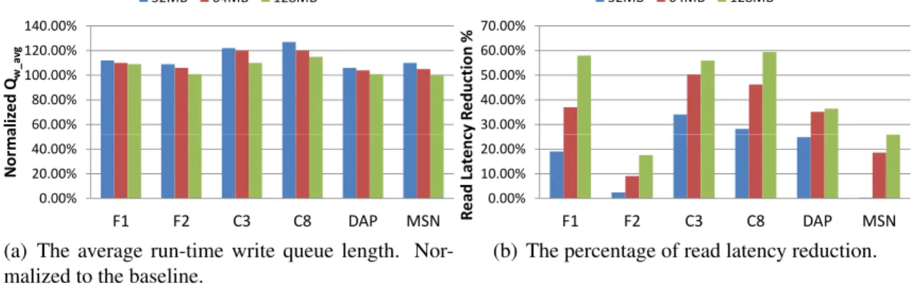
10 15 20 N o rm a li ze d Q w _ a v g 0 5 F1 F2 C3 C8 DAP MSN N o rm a li ze d Q
(b) The average run-time write queue length. Nor-malized to the baseline.
Figure 2.9: The read and write performance of the optimistic case: 100%N(vc) = 8
writes.
2.5.3
The Controlled Mode-switching of DiffECC
DiffECC switches among the proposed four write modes automatically regarding to the
immediate load of the drive. As discussed in Sec.2.4.3, we estimate the immediate load by
the number of pending requests and the expected idle slot time. In order to avoid interfering
with the future foreground requests (especially for the reads), we are required to service the
pending requests in the idle slots. At the mean time, we try to adopt slow write modes as
much as possible to boost the read performance. To achieve this goal, we first estimate
the time to fulfill the pending writes in each mode. For example, withNw page writes, the
takeTm2 = Lm2 ∗Nw, and so on. Lm1 andLm2 represent the write latency values of the
two modes, respectively. If the expected time for servicing the writes (Tidle avg −Tr, i.e.,
excluding the time to service the reads from the expected idle slot time) falls in between
two adjacent modes, for example, Tm2 andTm4, we would write Nm2 pages in the mode
“N(vc) = 2” and Nm4 pages in the mode “N(vc) = 4”, where Nm2 +Nm4 = Nw and
Nm2∗Lm2+Nm4∗Lm4 =Tidle avg−Tr.
With the above mode-switching policy, DiffECC successfully eliminates the overhead
on write throughput. As shown in Fig. 2.10(a), Qw avg of DiffECC (normalized to that
of the baseline) is increased by mostly less than 20% (except for C8 under 32MB cache,
that is because of the caching effect, i.e., more write hits, resulting longer idle slot time,
which helps smoothing the write workload further). As illustrated in Table2.4, the highest
Qw avg we observed in the baseline results is about 70. Given a flash page size of 4KB, the
overhead of less than 20% onQw avg means the I/O driver needs an extra amount of 56KB
(70∗20%∗4KB) memory to temporally hold the content of queued writes. Allocating and managing such a small piece of memory like 56KB is trivial compared to hundreds of
MB of buffer cache in the host side. Again, DiffECC causes higher overhead on C3 and C8
traces due to the same reason mentioned in the previous subsection. It is worth noting that
as the cache size increases from 32 MB to 128 MB, we observe less overhead.
However, comparing to the optimistic situation where we adopt 100% slowest writes,
the controlled mode-switching of DiffECC achieves less read latency performance gain.
As shown in Fig. 2.10(b), F1, C3, C8, and MSN approach the performance gain
upper-bound (Fig. 2.9) as the cache size increases from 32 MB to 128 MB, while under F2 and
DAP traces, DiffECC achieves relatively poorer gain. Particularly, DiffECC achieves the
60.00% 80.00% 100.00% 120.00% 140.00% N o rm a li ze d Q w _ a v g 32MB 64MB 128MB 0.00% 20.00% 40.00% F1 F2 C3 C8 DAP MSN N o rm a li ze d Q
(a) The average run-time write queue length. Nor-malized to the baseline.
30.00% 40.00% 50.00% 60.00% 70.00% R e a d L a te n cy R e d u ct io n % 32MB 64MB 128MB 0.00% 10.00% 20.00% F1 F2 C3 C8 DAP MSN R e a d L a te n cy R e d u ct io n %
(b) The percentage of read latency reduction.
Figure 2.10: The read and write performance of DiffECC with controlled mode-switching.
reduction percentage under 32 MB, 64 MB, and 128 MB is 18.1%, 32.8%, and 42.2%,
respectively. Generally speaking, the read latency performance of DiffECC is determined
by the available idle slots and the number of pending requests, which would determine the
ratio of each write modes used (thus the ratio of reads in each mode).
To have more insight about the observed read performance gain, we collect the
percentage of writes and reads in each mode and tune the cache size from 32 MB to 128
MB in Fig. 2.11 and Fig. 2.12, respectively. First of all, comparing the results of writes
and reads, we observe apparent resemblance between them in most traces except for MSN.
This is because of the extent of overlap between the working-set of writes and reads. We
have examined the extent of overlap in Table2.1usingW Rmaxas the metric: MSN has the
lowest W Rmax while the others are much more closer to 1. Second, looking at Fig.2.11,
as the cache size increases from 32 MB to 128 MB, we have more and more percentage of
slow write modes. That is due to the increased idle time resulted from less write workload
stress, which is in-turn caused by more write cache hits. F1 has more dramatic changes
(from baseline-mode dominated at 32 MB to slowest-mode dominated at 128 MB) than the
others due to a higher temporal locality existing in the writes. Third, with more slow mode
read latency reduction performance in Fig.2.10(b). For example, under F2 the dominate
read mode is constantlyN(vc) = 1with all three cache sizes and under MSN theN(vc) = 1
andN(vc) = 2modes outnumber the rests. Thus, DiffECC achieves less performance gain
under such two traces than the others.
20 30 40 50 60 70 80 90 100 % o f W r it e s i n E a c h M o d e N(vc)=1 N(vc)=2 N(vc)=4 N(vc)=8 0 10
F1 F2 C3 C8 DAP MSN F1 F2 C3 C8 DAP MSN F1 F2 C3 C8 DAP MSN
% o f W r it e s i n E a c h M o d e Cache size 32MB 64MB 128MB
Figure 2.11: Percentage of writes in each mode.
20 30 40 50 60 70 80 90 100 % o f R e a d s i n E a c h M o d e N(vc)=1 N(vc)=2 N(vc)=4 N(vc)=8 0 10
F1 F2 C3 C8 DAP MSN F1 F2 C3 C8 DAP MSN F1 F2 C3 C8 DAP MSN
% o f R e a d s i n E a c h M o d e Cache size 32MB 64MB 128MB
Figure 2.12: Percentage of reads in each mode.
To conclude the evaluation of DiffECC, we learned that un-controlled slow writes have
negative affects on the write throughput performance; using an workload adaptive method
of switching between slow and fast write modes, DiffECC successfully achieves a balance
2.6
Summary
In this work, motivated by the NAND flash memory device write speed vs. raw storage
reliability trade-off and run-time data access workload dynamics, we propose a cross-layer
co-design approach that can jointly exploit these features to opportunistically reduce SSD
read response latency. The key is to apply opportunistic memory write slowdown to enable
the use of shorter and weaker ECCs, leading to largely reduced SSD read latency. A
disk-level scheduling scheme has been developed to smooth the write workload to effectively
enable opportunistic memory write slowdown. To demonstrate its effectiveness, we use 2
bits/cell NAND flash memory with BCH-based error correction codes as a test vehicle. We
choose four different BCH coding systems. Extensive simulations over various workloads
show that this cross-layer co-design solution can reduce the average SSD read latency by
Chapter 3
Reducing SSD Access Latency via
NAND Flash Program and Erase
Suspension
3.1
Introduction
In NAND flash memory, once a page program or block erase (P/E) command is issued to a
NAND flash chip, the subsequent read requests have to wait until the time-consuming P/E
operation to complete. Preliminary results show that the lengthy P/E operations increase the
read latency by 2x on average. This increased read latency caused by the contention may
significantly degrade the overall system performance. Inspired by the internal mechanism
of NAND flash P/E algorithms, we propose a low-overhead P/E suspension scheme,
which suspends the on-going P/E to service pending reads and resumes the suspended
making writes be able to preempt the erase operations in order to improve the write latency
performance.
3.2
Motivation
In this section, we demonstrate how the read vs. P/E contention increases the read latency
under various workloads. We have modified MS-add-on simulator [3] based on Disksim
4.0. Specifically, under the workloads of a variety of popular disk traces, we compare
the read latency of two scheduling policies, FIFO and read priority scheduling (RPS), to
show the limitation of RPS. Furthermore, with RPS, we set the latency of program and
erase operation to be equal to that of read andzeroto justify the impact of P/E on the read
latency.
3.2.1
A Simple Demonstration of Contention Effect
First of all, we illustrate the contention effect between reads and writes with an simple
example. Figure 3.1 shows the timing diagram of one flash chip servicing three read
requests (RD) and one write request (WT), of which the arrival time is marked on the
top timeline. The raw latency of read and write is assumed to be one and five time units,
respectively. Three scheduling policies, FIFO, RPS, and RPS+Suspension, are analyzed
under this workload. With FIFO, both RD2 and RD3 are scheduled for service after the
completion of WT1, resulting service latency of 6 and 4 units. RPS schedules RD2 ahead
of WT1. However, RD3 has to wait until WT1 is serviced because suspension of write
is not allowed. RPS+Suspension is our desired solution for this problem where WT1 is
![Figure 1.3: Control Logic Block [10]](https://thumb-us.123doks.com/thumbv2/123dok_us/1356417.2681452/18.918.277.699.613.893/figure-control-logic-block.webp)
![Figure 1.4: Typical SSD Architecture [60].](https://thumb-us.123doks.com/thumbv2/123dok_us/1356417.2681452/19.918.283.696.158.385/figure-typical-ssd-architecture.webp)