University of Rhode Island University of Rhode Island
DigitalCommons@URI
DigitalCommons@URI
Open Access Dissertations
2019
In storage process, the next generation of storage system
In storage process, the next generation of storage system
Dongyang LiUniversity of Rhode Island, [email protected]
Follow this and additional works at: https://digitalcommons.uri.edu/oa_diss
Recommended Citation Recommended Citation
Li, Dongyang, "In storage process, the next generation of storage system" (2019). Open Access Dissertations. Paper 839.
https://digitalcommons.uri.edu/oa_diss/839
This Dissertation is brought to you for free and open access by DigitalCommons@URI. It has been accepted for inclusion in Open Access Dissertations by an authorized administrator of DigitalCommons@URI. For more information, please contact [email protected].
PROCESSING IN STORAGE, THE NEXT GENERATION OF STORAGE SYSTEM
BY
DONGYANG LI
A DISSERTATION SUBMITTED IN PARTIAL FULFILLMENT OF THE REQUIREMENTS FOR THE DEGREE OF
DOCTOR OF PHILOSOPHY IN
ELECTRICAL ENGINEERING
UNIVERSITY OF RHODE ISLAND 2019
DOCTOR OF PHILOSOPHY DISSERTATION OF
DONGYANG LI
APPROVED:
Dissertation Committee:
Major Professor Qing Yang Jien-Chung Lo Lutz Hamel Manbir Sodhi Nasser H. Zawia
DEAN OF THE GRADUATE SCHOOL
UNIVERSITY OF RHODE ISLAND 2019
ABSTRACT
In conventional computer systems, software relies on the CPU to handle the process applications and assign computation tasks to heterogeneous accelerators such as GPU, TPU and FPGA. It requires the CPU to fetch data out of the storage device and move the data to the heterogeneous accelerators. After the accelerators complete computation tasks, the results are flushed to the main memory of the host server for software applications. In this architecture, the heterogeneous accel-erators are located far away from the storage device. There are data movements on the system bus (NVM-express/PCI-express), which requires a lot of transmission time and bus bandwidth. When data move back and forth on the storage data bus, it decreases the overall performance of the storage system.
This dissertation presents the in-storage processing (ISP) architecture that offloads the computation tasks into the storage device. The proposed ISP archi-tecture eliminates the back and forth data movements on the system bus. It only delivers the computation results to the host memory, saving the storage bus band-width. The ISP uses FPGA as a data processing unit to process computation tasks in real-time. Due to the parallel and pipeline architecture of the FPGA implemen-tation, the ISP architecture processes data in short latency, and it has minimal effects on the data flow of the original storage system.
In this dissertation, we proposed four ISP applications. The first ISP appli-cation is the Hardware Object Deserialization in SSD (HODS), which is designed to tailor to the high-speed data conversion inside the storage device. The HODS shows visible differences compared to software object deserialization regarding ap-plication execution time while running Matlab, 3D modeling, and other scientific computations. The second ISP application is called the CISC: Coordinating Intelli-gent SSD and CPU. It speeds up the Minimum Spanning Tree (MST) applications
in graph processing. The CISC coordinates the computing power inside SSD stor-age with the host CPU cores. It outperforms the traditional software MST by 35%. The third application speeds up the data fingerprint computation inside the storage device. By pipelining multi data computation units, the proposed archi-tecture processes the Rabin fingerprint computation in wire speed of the storage data bus transmission. The scheme is extensible to other types of fingerprint/CRC computations and readily applicable to primary storage and caches in hybrid stor-age systems. The fourth application is data deduplication. It eliminates duplicate date inside the storage and provides at least six times speedup in throughput over software.
The proposed ISP applications in this dissertation prove the concept of com-putational storage. In the future, more compute-intensive tasks can be deployed into the storage device instead of processing in the CPU or heterogeneous accel-erators (GPU, TPU/FPGA). The ISP is extensible to the primary storage and applicable for the next generation of the storage system.
ACKNOWLEDGMENTS
There are so many people to thank during my Ph.D. study at URI. So many have made my stay here productive and pleasant. I will try to cover all the bases without long-winded words.
Foremost, I would like to thank my advisor and mentor, Dr. Ken (Qing) Yang, for his guidance, encouragement, and inspiration over the past seven years. Dr. Yang has introduced me to the wonderland of research. He has helped me thrive in academia and life. He has taught me crucial skills in writing and presenting and, more importantly, the ways of doing research, which benefits throughout my life. His support has been essential to my success in the Ph.D. program at URI; it paved the way to this dissertation.
I would like to thank Dr. Jien-Chung Lo for providing me with constructive suggestions and feedback during my academic journey. I would like to thank Dr. Lutz Hamel from the Department of Computer Sciences, for introducing me to the machine learning algorithm. Much appreciations go to Dr. Manbir Sodhi, who has advised me on my dissertation, and Dr. Haibo He, the department chair, who has encouraged me and given me insightful suggestions on my research and future career. I sincerely thank them all for their support and feedback to improve this dissertation.
I would like to thank my collaborators, Jing Yang and Shuyi Pei. We have worked on the architecture of memory and storage system. They have introduced me to the FPGA, kernel driver and software developing. They have also advised me on writing and revising my manuscripts. I sincerely thank them for their support and help during my study at URI.
I would also like to thank many professors and staffs in URI ECBE depart-ment. I learn from many of them via different courses, which equipped me with
knowledge to tackle problems in this dissertation and my future career. The de-partment staffs were very helpful, especially Meredith Leach Sanders and Lisa Pratt. They helped me to deal with paperwork and showed me concrete guidance of academic affairs.
I would like to express my thanks to my girlfriend Bing Han who is the Ph.D. student of Texas A&M University. She is always there cheering me up, and stand-ing by me through good times and bad.
Finally, none of these would have been possible without the patience and support of my family. I would like to express my heartfelt thanks to my family. My parents raised and educated me with their unconditional love, and supported me to complete this degree. I regret to have less time to accompany with my family during my Ph.D. study. I will cherish everyone who appears in my life.
PREFACE
This dissertation is organized in the manuscript format. Particularly, there are four manuscript chapters. A brief introduction of the manuscripts are as follows:
Manuscript 1: Dongyang Li, Fei Wu, Yang Weng, Qing Yang, Changsheng Xie, ”HODS: Hardware Object Deserialization Inside SSD Storage,” 2018 IEEE 26th Annual International Symposium on Field-Programmable Custom Computing Ma-chines (FCCM), Boulder, CO, USA, 2018, pp. 157-164.
Manuscript 2: Dongyang Li, Weijun Li, Qing Yang, ”CISC: Coordinating In-telligent SSD and CPU to Speedup Graph Processing,” 2018 17th International Symposium on Parallel and Distributed Computing (ISPDC), Geneva, Switzer-land, 2018, pp. 149-156.
Manuscript 3: Dongyang Li, Qingbo Wang, Cyril Guyot, Ashwin Narasimha, Dejan Vucinic, Zvonimir Bandic, Qing Yang, ”A Parallel and Pipelined Architec-ture for Accelerating Fingerprint Computation in High Throughput Data Stor-ages,” 2015 IEEE 23rd Annual International Symposium on Field-Programmable Custom Computing Machines (FCCM), Vancouver, BC, Canada, 2015, pp. 203-206.
Manuscript 4: Dongyang Li, Qingbo Wang, Cyril Guyot, Ashwin Narasimha, Dejan Vucinic, Zvonimir Bandic, Qing Yang, ”Hardware accelerator for similarity based data dedupe”, 2015 IEEE International Conference on Networking, Archi-tecture and Storage (NAS), Boston, MA, USA, 2015, pp 224-232
TABLE OF CONTENTS
ABSTRACT . . . ii
ACKNOWLEDGMENTS . . . iv
PREFACE . . . vi
TABLE OF CONTENTS . . . vii
LIST OF FIGURES . . . xi
LIST OF TABLES. . . xiv
MANUSCRIPT 1 HODS: Hardware Object Deserialization in side SSD Storage 1 1.1 Abstract . . . 2
1.2 Introduction . . . 2
1.3 Motivation of hardware deserialization . . . 5
1.4 Hardware Deserialization SSD Architecture . . . 10
1.4.1 System Architecture . . . 10
1.4.2 FPGA object deserialization module . . . 10
1.4.3 Host Driver Program . . . 14
1.5 Experimental Methodology . . . 15
1.5.1 Experimental platform . . . 15
1.5.2 Benchmarks . . . 16
1.6 Evaluation results . . . 16
Page
1.6.2 Throughput speedup . . . 18
1.6.3 Speedup of Application Execution Time . . . 19
1.7 Conclusion . . . 20
List of Reference . . . 21
2 CISC: Coordinating Intelligent SSD and CPU to Speedup Graph Processing . . . 23
2.1 Abstract . . . 24
2.2 Introduction . . . 24
2.3 Background . . . 28
2.3.1 Overhead of Sorting in MST . . . 28
2.3.2 Previous Work on Near-Data Processing . . . 29
2.4 Hardware Architecture of In-storage Sort . . . 30
2.4.1 System architecture . . . 30
2.4.2 In-storage sort module . . . 31
2.5 Software Design of CISC . . . 34
2.5.1 Serial CISC software . . . 35
2.5.2 Parallel CISC software . . . 36
2.6 Evaluation . . . 39
2.6.1 Experimental Platform and Benchmark Selection . . . . 39
2.6.2 Numerical Results and Discussions . . . 40
2.6.3 Hardware Cost Analysis . . . 42
2.7 Conclusion . . . 43
Page 3 A Parallel and Pipelined Architecture for Accelerating
Fin-gerprint Computation in High Throughput Data Storages . . 47
3.1 Abstract . . . 48
3.2 Introduction . . . 48
3.3 Background and architectural overview . . . 50
3.3.1 Pipelining with Fresh and Shift stages . . . 51
3.3.2 Sampling of Fingerprints . . . 52
3.4 Designe and optimization . . . 53
3.4.1 Rabin Fingerprint Pipeline Design . . . 53
3.4.2 Channel Sampling and Final Selection . . . 54
3.4.3 Parallel Pipelines . . . 55
3.5 Implementation and evaluation . . . 56
3.5.1 Hardware Implementation Evaluation . . . 56
3.5.2 Software Comparison . . . 57
3.6 Conclusion and future works . . . 58
List of Reference . . . 59
4 Hardware Accelerator for Similarity Based Data Dedupe . . 60
4.1 Abstract . . . 61
4.2 Introduction . . . 61
4.3 Background . . . 64
4.3.1 Standard dedupe . . . 64
4.3.2 Similarity based dedupe . . . 64
4.3.3 Delta compression . . . 65
Page
4.4.1 Compute Sketches . . . 65
4.4.2 Reference block index . . . 67
4.4.3 Delta compression . . . 69
4.5 Implementation and evaluation . . . 73
4.5.1 Experimental setup . . . 73
4.5.2 Latency . . . 74
4.5.3 Data Reduction Ratio . . . 78
4.6 Conclusion and future works . . . 79
LIST OF FIGURES
Figure Page
1 An example ASCII file. . . 6
2 Fractions of object deserialization time over total running time of applications. . . 7
3 General data flow of existing PIS functions inside an SSD device. 7 4 Comparison of object deserialization throughput between em-bedded ARM inside SSD and host CPU. . . 8
5 FPGA based object deserialization model. . . 9
6 HODS architecture of FPGA based NVM-e storage. . . 11
7 Hardware object deserialization diagram. . . 11
8 Pipeline stages of hardware object deserialization . . . 13
9 Normalized size variation after hardware deserialization. . . 17
10 Throughput comparison between hardware object deserializa-tion and host software soludeserializa-tion. . . 18
11 Normalized hardware deserialization speedup. . . 19
12 Fractions of graph sort time over total execution time of the serial and parallel MST running on multi-cores. . . 28
13 System architecture of the CISC. . . 31
14 The architecture of the linear-time sorter. . . 32
15 The pipeline architecture of the in-storage sort module. . . 33
16 MST software of CISC on the single-core system. . . 35
17 CISC optimizes sample sort algorithm in MST. . . 37
18 The sort speedup of CISC, the baseline is serial software sort running on single-core. . . 40
Figure Page
19 The MST speedup of CISC, the baseline is serial MST running
on single-core. . . 42
20 The diagram of shingles. . . 50
21 Pipeline with the fresh and shift stages. . . 51
22 Design with fingerprint pipeline and signature selection. . . 53
23 Rabin fingerprint pipeline. . . 54
24 Channel sampling (a) and Final selection (b). . . 55
25 Parallel pipelines. . . 56
26 Primary storage prototype. . . 57
27 Hardware and software comparison: (a) Latency (b) Throughput. 58 28 An example showing two shingles. . . 66
29 Rabin fingerprint pipeline. . . 67
30 Block diagram of hardware design for sketch computation with fingerprint pipeline and sketch selection. . . 68
31 Block diagram of hardware cuckoo hash search engine. . . 69
32 Parallel search structure for reference block index. . . 70
33 An example showing hardware delta compression encoding. . . . 71
34 Delta compression engine for every 8-byte data quantum. . . 72
35 Parallel delta compression structure for every one byte shift shingles. . . 73
36 Experiment platform for hardware accelerating similarity based data deduplication. . . 74
37 Sketch computing time on three datasets. . . 75
38 Average latencies of reference block search for different similar-ity thresholds. . . 76
Figure Page
39 Delta compression time comparison between hardware and soft-ware with different thresholds. . . 77 40 Similarity based data reduction comparison between hardware
and software for three datasets with different similarity thresholds. 78 41 Comparison between standard dedupe and hardware dedupe for
LIST OF TABLES
Table Page
1 Comparison of the serial sort between software and CISC . . . . 36 2 The Benchmark datasets we used in this paper . . . 40 3 Hardware resource utilization of CISC on different FPGAs . . . 43 4 Design Complexity Comparison . . . 52 5 Synthesis Report (Fingerprint + Sampling) . . . 56
MANUSCRIPT 1
HODS: Hardware Object Deserialization in side SSD Storage
by
Dongyang Li1, Fei Wu2, Yang Weng3, Qing Yang4, Changsheng Xie5
is published in the 26th Annual International Symposium on
Field-Programmable Custom Computing Machines (FCCM), Boulder, 2018.
1Ph.D Candidate, Department of Electrical, Computer and Biomedical Engineering, The
University of Rhode Island, Kingston, RI 02881. Email: [email protected]
2Associate Professor, School of Computer Science and Technology, Huazhong University of
Science and Technology. Email: [email protected]
3Master student, School of Computer Science and Technology, Huazhong University of Science
and Technology. Email: [email protected]
4Distinguish Professor, Department of Electrical, Computer and Biomedical Engineering, The
University of Rhode Island, Kingston, RI 02881. Email: [email protected]
5Department Dean, School of Computer Science and Technology, Huazhong University of
1.1 Abstract
The rapid development of nonvolatile memory technologies such as flash, PCM, and Memristor has made processing in storage (PIS) a viable approach. We present an FPGA module augmented to an SSD storage controller that provides wire-speed object deserialization, referred to as HODS for hardware object deseri-alization in SSD. A pipelined circuit structure was designed to tailor to high-speed data conversion specifically. HODS is capable of conducting deserialization while data is being transferred on I/O bus from the storage device to host. The FPGA module has been integrated with our newly designed NVM-e SSD. The working prototype demonstrated significant performance benefits. The FPGA module can process data in line speed at 100MHz on 16 Byte data stream. For integer bench-marks, HODS showed deserialization speedup of 8∼12×as compared to the tradi-tional deserialization on a high-end host CPU. The speedup can reach 17∼21×for floating-point datasets. The measured object deserialization throughput is 1GB/s on average at a clock speed of 100MHz. The overall performance improvements at the application level range from 10% to a factor of 4.3× depending on the proportion of deserialization time over total application running time. Compared to traditional SSD on the same server, HODS showed visible differences regard-ing application execution time while runnregard-ing Matlab, 3D modelregard-ing, and scientific computations.
1.2 Introduction
Object deserialization is a process of creating data structure suitable for appli-cations. It can spend 64% of the total execution time of an application on average if the traditional deserialization process is used [1]. It typically takes three steps: (1) Raw data is read out of storage device and buffered in the host memory; (2) Host CPU transforms raw data into binaries; (3) Application computation executes
using binary results of object deserialization. This CPU-centric approach becomes inefficient for several reasons: First of all, step 2 cannot take full advantages of modern CPUs, because the scanning access of a significant amount of data has poor data locality making the deep cache hierarchy useless. Secondly, it suffers from considerable overhead in the host system because of frequent context switch-ing caused by significant amount of storage I/Os [2]. Finally, host deserialization intensifies the bandwidth demand of both I/O interconnect and CPU-memory bus which may create I/O bottleneck problem.
Realizing the inefficiencies of host-based object deserialization, researchers have tried to offload such operations to data storage. Tseng et al. presented Mor-pheus that can substantially speed up benchmark applications using processing in storage (PIS) [1]. By making use of the simpler and more energy-efficient processors found inside SSD devices, Morpheus frees up scarce CPU resources that can either do more useful work or be left idle to save energy. At the same time, it consumes less bus bandwidth than the conventional system. While Morpheus demonstrated 1.66×speedup by using embedded processor inside SSD device to carry out object deserialization, it consumes the scarce resource of the SSD controller cores that are meant to carry out FTL, wear leveling, garbage collection, and flash control functions. Besides, the device I/O path is slowed down by the firmware process because of embedded processor’s overhead and buffering of intermediate results in ARM D-Cache [3].
This paper presents a hardware approach to providing wire-speed object de-serialization, referred to as HODS, hardware object deserialization in SSD storage. We have designed and implemented an FPGA module that is augmented in an SSD along the I/O path to carry out the necessary data conversion. It works in paral-lel with all storage operations and conducts real-time computation with pipelined
structure. Instead of buffering intermediate results, our FPGA solution converts the data while data is transferred from storage to the host. Therefore, it eliminates the slow down of read I/Os from the SSD storage. HODS brings several benefits compared to the previous solutions: (1) It substantially speeds up host CPU exe-cution time because of PIS. (2) Our architecture eliminates extra memory accesses between embedded processors and its D-Cache memory hierarchy. (3) This new approach is extensible to execute other computations such as object search, image processing and machine learning, all of them can be easily integrated into current storage ASIC design.
To demonstrate the feasibility and effectiveness of HODS, we have built an FPGA prototype based on an NVM-e [4] SSD storage card with PCI-e Gen3×4. The FPGA SSD controller runs at a 100MHz clock with the bus width of 16 bytes. The HW deserialization module is attached along the 16 bytes bus capable of processing 16 bytes of data in parallel per clock cycle. Data conversion is done concurrently with data transfer on the bus when NVM-e command directs the SSD to do so. Such NVM-e directives are passed along from the host NVM-e driver down to the SSD device. To allow applications to use such functions, we have modified the host NVM-e driver to support our prototype implementation. The working prototype SSD is used to carry out performance measurement experiments. Our measurement results show that HODS accelerates object deserialization by 8 to 12× as compared to host CPU execution time for integer data. For floating point data, the speedup ranges from 17 to 21×for deserialization operations. The overall speedup for applications depends on the fraction of deserialization time over the total execution time of benchmarks. For BigDataBench, Rodinia and JAPSPA benchmark applications, we observed an overall speedup of 10% to a factor of 4.3×. Compared to traditional SSD on the same server, HODS showed visible differences
in terms of application execution time while running Matlab, 3D modeling, and scientific computations. The demo video for the Matlab application can be found on YouTube at [5].
This paper makes the following contributions: (1) It presents an FPGA dese-rialization module that can provide wire-speed data conversion. We have designed and implemented the FPGA module alongside the I/O bus inside a PCI-e SSD card using NVM-e protocol. (2) It realized a PIS function in a modern SSD stor-age and offered practical benefits to applications. It is also extensible to other PIS functions. (3) A working prototype has been built to be functional running at a clock speed of 100MHz. Even at this low clock speed, it provides data conversion speed of 1GB/s. (4) Extensive performance measurements have been carried out to demonstrate the performance and effectiveness of HODS.
The rest of this paper is organized as follows: Section II describes the moti-vation of hardware deserialization and its corresponding performance issues. Sec-tion III provides detailed design for FPGA object deserializaSec-tion module including hardware PIS storage architecture, FPGA object deserialization module, and host programming API. Section IV describes the experimental prototype implementa-tion. Section V reports performance results. We conclude our paper in Section VI.
1.3 Motivation of hardware deserialization
Most non-database applications such as scientific data analytics, 3D modeling, or spreadsheet applications use interchangeable data formats such as ASCII code. Such serialized memory objects make it easy to collect, exchange, transmit, or store data [2] because the text-based (e.g., CSV [6], txt) encodings allow machines with different architectures (e.g., little endian vs. big endian) to exchange data with each other. It does not require users to understand memory layout of machines,
Figure 1. An example ASCII file.
and it is often easy to manage text-based encoding files without using special editing tools.
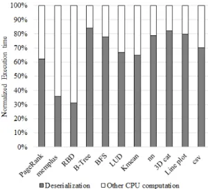
Figure 1 shows an example of a standard ASCII file chunk. Meaningful ASCII strings are stored between special characters such as space, line-feed, and comma. Before any computation can be done on the data, such text-based encoding strings must be converted into machine binaries readable by applications [7]. To under-stand how such data conversion affects the overall application performance, we ran a set of benchmarks on a Lenovo server with a quad-core Intel i7-4470 CPU. The benchmark datasets are stored in an Intel 750 series NVM-e SSD. In this experi-ment, each benchmark application reads the data file from the SSD, converts the file from text to binary in the system RAM, and then processes the data. Figure 2 shows the breakdown of the execution time of the benchmark applications [7, 19, 20]. It can be seen from the figure that the object deserialization (data conversion) takes a significant proportion of the total execution time of applications, ranging from 32% to 85%.
To minimize the overhead of host CPU, object deserialization in PIS has been proposed in flash memory SSDs [1]. Figure 3 illustrates general data flow inside current PIS storage [8∼16]. First, SSD controller loads data from flash to D-Cache using DMA (step 1); Next, the embedded processors (such as ARM core) fetch data from D-Cache and execute PIS functions (step 2). After that, the embedded cores
Figure 2. Fractions of object deserialization time over total running time of appli-cations.
write PIS results back into D-Cache (step 3). Finally, host fetches PIS results from the D-Cache to host main memory through NVM-e/PCI-e interconnect (step 4). Although current PIS storage can offload host object deserialization to SSD controller, following limitations exist:
Back and forth accesses of D-Cache stall standard storage IO path. As shown in Figure 3, step 2 and step 3 slow down the I/O operations. Because moving data in and out of D-Cache takes time, and it interrupts standard I/O flow. In conventional PCI-e or NVM-e SSD, storage data can directly move from flash to host main memory by one DMA operation [1, 9, 10]. Because of this PIS architecture, it breaks single DMA data movement into two sub DMA operations.
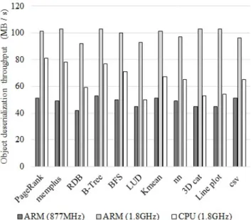
Figure 4. Comparison of object deserialization throughput between embedded ARM inside SSD and host CPU.
One goes in D-Cache, and the other goes out of D-Cache. This modification blocks IO path and slows down storage read speed [17, 18].
PIS using Embedded cores in SSD is not efficient enough. To verify the ac-tual efficiency of using embedded cores for object deserialization, we experimented with ARM Cortex-A9 processor with two different clock settings. As shown in Figure 4, single ARM with 877MHz clock speed can provide 42∼53MB/s through-put on both integer and floating-point benchmarks [19, 20]. There is not much throughput difference between integer and floating-point because of FPU (float-ing point unit) inside ARM processor in our experiment. Object deserialization throughput increases to 91∼104MB/s when setting ARM clock to 1.8GHz. To make a comparison with the host server, we choose Xeon E5 CPU with 1.8GHz to run the same benchmarks. The host was set up with Linux Ubuntu 16.04. The benchmarks are cached in the host DRAM before the object deserialization execu-tion. Our measurement results show that ARM accelerates object deserialization by 1.25∼1.76× as compared to host CPU execution time when set to the same
Figure 5. FPGA based object deserialization model.
clock speed. However, current NVM-e/PCI-e bandwidth can reach 4GB/s (e.g., PCI Express Gen3x4). Therefore, there is still a plenty of room for performance improvement for PIS.
In addition to the speed limitations, the embedded cores inside SSD are mainly used for control functions such as FTL, wear leveling, garbage collection, and flash control functions. These controller functions already consume a lot of computing resources of the embedded cores. Adding additional processing tasks for the PIS functions may overload the cores and adversely impact the I/O performance.
D-Cache resource is limited. D-Cache is the precious resource inside a flash SSD controller and its size is limited. The major function of D-Cache inside SSD is to cache FTL table and a small amount of hot data. Because of D-Cache size limitations, flash controller can neither buffer a large amount of data to be converted nor can it hold many intermediate values during PIS processing. Most existing PIS storage systems frequently access D-Cache, increasing the workload of a flash controller and dragging down PIS throughput at the same time [9, 17, 21, 22].
From the above discussions, it is clear that doing object deserializations using software running on embedded cores has limited performance gain. Hardware FPGA accelerators are desirable to speed up such necessary processing step. Our HODS architecture aims at offering such acceleration without slowing down I/O
operations. It does not take away scarce resources from SSD controller cores.
1.4 Hardware Deserialization SSD Architecture
Figure 5 depicts the time slices of FPGA based HODS design. Compared to previous architecture in Figure 3, there is no supefluous memory access to store and fetch intermediate results [23, 24]. We build a direct IO path from storage to host main memory, and PIS is done concurrently with data transfer on the bus. In the following paragraphs, we will describe system architecture, hardware object deserialization module, and host driver program in detail.
1.4.1 System Architecture
Figure 6 shows the overall architecture of the SSD with the hardware PIS for object deserialization. The SSD contains DDR3 for data caching and flash translation layer (FTL). All the storage control functions are implemented on an FPGA. Inside the FPGA chip, major storage logic units include three embedded cores, DRAM/flash controller, NVM-e logic interface, DMA/cache engine and PIS function for hardware object deserialization. All modules are connected to AXI4 bus which is a bridge for data movement among host, flash and DDR3. As the flash controller processor, three embedded cores are responsible for standard storage control workflow. They do not get involved in PIS processing, but only direct storage data flow to go through FPGA object deserialization module.
1.4.2 FPGA object deserialization module
To extract meaningful data structure from ASCII files, we designed and im-plemented hardware deserialization module. As shown in Figure 7, the hardware object deserialization module is a four-stage pipeline. The first stage pipeline is to search special characters such as space, line-feed, and comma along with n bytes parallel data stream. The special characters’ location information will be passed
Figure 6. HODS architecture of FPGA based NVM-e storage.
down to the next pipeline stage. The second stage figures out how many object characters are between two special characters. The third stage pipeline converts objects to integer or floating point, and it can bypass ASCII string. At last, ob-ject data assembler collects all deserialization results fromn parallel modules from stage three. Final object deserialization results are sent to the NVM-e interface directly.
Special character search engine: We search every byte along withn-byte width data stream in each clock cycle, which requiresn parallel search units to keep pace with the wire speed. Each search unit corresponds to 1-byte comparator in the circuit. The output of special character search engine is a channel enable switch of the second stage pipeline: object length detector, as shown in upper part of Figure 8.
Object length detector: Input data stream splits inton sliding windows (shin-gles) as shown at the top part of Figure 8. Each shingle contains m×n bytes,
where m is an integer that m×n indicates the maximum object length we can detect between every two special characters. The output from pipeline stage one indicates which shingle’s first byte hits special character such as space, line-feed or comma. If a shingle’s first byte hits a special character or current shingle is the start shingle of a data file, its length detector is enabled to search the next nearest special character. Otherwise, corresponding shingle length detector is disabled.
Because every first byte of each shingle is used to enable/disable shingle length detector, it requiresm×n-1 comparators to work in parallel for the remaining bytes along with the rest shingle content. All comparators’ results are assembled into low address arbiter to find out object length from the start byte of the shingle. If shingle’s first byte is not a special character, object length detector will disable current shingle output.
The m×n-1 comparators also detect the location of the decimal point. According to the binary values of the shingle content, the object length detector identifies the type of shingle data (integer, floating point or ASCII string) and passes down the shingle type to the object converter along with the object length, shingle content and decimal location.
Object converter: n shingle converters are working in parallel, each one of them processes three types of the shingle data: the floating point shingle is converted to the floating point data by FPU [27]; the ASCII string shingle bypass; the integer shingle goes to the multiplexer matrix. As shown in the middle part of Figure 8, each integer shingle converter is composed of a multiplexer matrix. Each column of multiplexers shares the same weight of multiplicand such as times one thousand or times one hundred.
row first fetches shingle content to its local buffer and converts ASCII to binary for each byte in the shingle. Secondly, each shingle byte multiplies corresponding multiplicand weight. Finally, selected row sums up all weight values together as converted results. To optimize hardware resource in FPGA implementation, we turned such multiplexer matrix into table lookup structure, which precomputes multiply values and stores into lookup tables. It saves 70% logic resources com-pared to multiplexer matrix.
Object data assembler: As shown at the bottom part of Figure 8, object data assembler is the collector of n parallel shingles. The output results from the third stage pipeline are fixed size binaries. Object data assembler sequentially buffers such binaries inton-input/1-output RAM. Once the write count of the buffer RAM exceeds a threshold value, e.g., half of RAM size count, RD address generator starts to read binary results out of RAM and flushes data to NVM-e interface. Newly converted results can still be buffered by writing into another half of RAM address. It grantees all the converted results can be flushed into NVM-e interface without halt.
1.4.3 Host Driver Program
To allow an application to use the hardware object deserialization module, we have developed a programming framework including libraries and NVM-e driver modifications using C/C++ programming languages. This section will briefly in-troduce our driver program and show how our driver interacts with hardware object deserialization module.
On the driver side, NVM-e is a scalable host controller interface developed specially for accessing non-volatile memory attached via PCI-e bus. It includes support for parallel operation by supporting up to 64K commands within a single I/O queue to the device. NVM-e encodes commands into 64-byte packets and
uses one-byte command opcode [4]. We modified original host NVM-e module by adding one-bit flag opcode into NVM-e read command. Other commands remain unchanged. The newly added flag bit is a switch to determine whether the storage internal data flow bypasses or goes through the object deserialization module. If the flag bit is not set, SSD controller initiates DMA to move data from flash to host main memory. Otherwise, SSD controller directs flash data to go through hardware deserialization module and sends results to e interface. Our NVM-e drivNVM-er doNVM-es not touch thNVM-e original submission and complNVM-etion quNVM-euNVM-e stratNVM-egy, and modification effort is minimal.
In host application, original C/C++ object deserialization functions such as (fscanf) or (sscanf) are replaced by our application function (HODS scanf). The HODS converts all variation sized ASCII strings into fix sized binaries and se-quentially stores such binaries into host main memory. Our application func-tion (HODS scanf) sequentially access host main memory to fetch results directly, which substantially offloads host CPU’s workload.
1.5 Experimental Methodology
We have built an NVM-e SSD prototype that supports hardware object dese-rialization and carried out performance evaluation using several standard bench-marks. This section discusses the prototype setup and benchmark selection.
1.5.1 Experimental platform
The experimental platform uses Lenovo server with a quad-core Intel i7-4470 running at 3.4 GHz. The system DRAM size is 32 Gbyte. The host was set up with Linux Ubuntu 16.04, kernel version 4.4. Our prototype NVM-e SSD card plugs into host server through PCI-e Gen3x4 interconnect.
stor-age card [5]. All storstor-age logic fits into a single FPGA chip, including embedded processors, DRAM/flash controller logic, NVM-e module, DMA/cache engine and hardware deserialization function. This prototype card contains 8Gbyte DDR3 and 1TB flash memory. To evaluate HODS, we store benchmark dataset on 1TB flash before host starts applications. The following paragraph describes benchmark we used in this paper.
1.5.2 Benchmarks
We selected benchmarks from BigDataBench [20], JASPA [7] and Rodinia [19] with following criteria: (1) The input data of applications are text files. (2) Large and meaningful inputs data can be generated from benchmark tools for our evaluation. (3) The application contains many floating point values that we can evaluate our prototype comprehensively. (4) The application is open source in C programming that is compatible with our prototype. Benchmark applications may apply MPI [25] or openMP [26] to parallelize host computation. Some appli-cations provide data generators such as LU-decompression (LUD), Breadth First Search (BFS), K-mean and B-tree. Other datasets are generated by duplicating benchmark input data. We also provide 3D plot application to demonstrate user experiences of using HODS as compared to existing systems [5]. All benchmark program codes are written in C/C++, and we use Verilog to generate RTL for FPGA.
1.6 Evaluation results
For the purpose of comparative analysis, we consider the baseline as running applications on the server machine with HODS disabled. Using the same server machine, we enable HODS and run the same set of applications to evaluate per-formance.
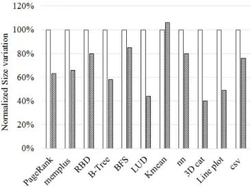
Figure 9. Normalized size variation after hardware deserialization.
1.6.1 Transfer size variation
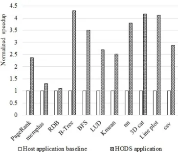
Figure 9 shows data size changes after FPGA object deserialization. Transfer size shrinks because text-based encoding usually requires more bytes than binary representations. For example, ASCII string ”87654321” requires 8 bytes to repre-sent a single object value, but it is only 4 bytes in binary. The longer object is, the smaller converted data size will be. We also eliminate special characters such as space, line-feed and comma, which are unneeded data for benchmark applications. The size variations of PageRank, memplus, BFS, B-tree and nearest neighbor decreased 15%∼41% after going through the hardware deserialization module. LU-decompression, line plot and 3D cat benchmarks are floating point only. The average object length is 8∼9 bytes each. As a result, the transmitted data size reduces by 51%∼60% after hardware object deserialization. The size variation of Kmean increased 6% after hardware deserialization. Because half of ASCII strings in Kmean are single byte length, data size expands when using 32-bit binary to represent single byte ASCII string.
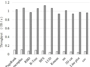
Figure 10. Throughput comparison between hardware object deserialization and host software solution.
I/O bus burden while running applications that require a large data set. It also reduces the IOPS (I/Os Per Second) requirement of the SSD by the applications. Taking PageRank application as an example, a 600K IOPS SSD with HODS would perform the same as a 1 million IOPS SSD without HODS.
1.6.2 Throughput speedup
Figure 10 plots the data conversion throughput. HODS accelerator achieves as much as 935MB/s∼1.13GB/s object deserialization throughput in 100MHz FPGA clock, and host CPU has 58MB/s∼93MB/s throughput at 3.5GHz clock speed. For integer benchmarks such as PageRank, memplus, B-tree and BFS, we ob-served 8∼12× speedup. These Performance gains can be attributed to two facts. First, it provides at least 100Mhz-16Byte wire-speed processing in HODS. Sec-ondly, resultant data size decreased 15%∼41% after FPGA object deserialization. It can potentially reduce the storage traffic overhead.
Because host CPU takes much longer time to convert floating point numbers from ASCII code, HODS’ speedup is even higher for floating point benchmarks such
Figure 11. Normalized hardware deserialization speedup.
as LU-decompression, 3D-cat and line plot. Furthermore, data sizes of floating point benchmarks are also reduced by 51%∼60%, giving rise to more speedup. From our experiments, we observed speedup between 17×and 21×. In both integer and floating point object deserializations, HODS runs faster than the existing state of art [1] that has shown 1.66× for the same benchmarks.
1.6.3 Speedup of Application Execution Time
The overall speedup of application programs depends on the fraction of data conversion time over benchmark applications’ running time. Our work focuses on object deserialization itself. If benchmark application is computation intensive, the data conversion becomes a small fraction of total time. Then its performance improvement is limited.
Figure 11 plots the HODS’ speedup of applications. Benchmarks such as RDB and memplus give only 10% to 30% speedup because they contain matrix multipli-cation which is computation intensive. The other benchmark applimultipli-cations showed 2.4∼4.3× speedup. Current benchmark applications apply MPI or OpenMP
par-allel model with quad-cores. We expect higher speedup when using more cores or GPUs that run the computation part in parallel but can hardly do anything on data conversion part. Quantitative investigation on such parallel computer architectures is out of our research scope of this paper.
1.7 Conclusion
This paper presents a hardware object deserialization in SSD (HODS) that offloads data-intensive computation to storage where data is stored. Compared to existing state of art [1], HODS eliminates SSD controller’s overhead and buffer limitations. It can process storage data in wire speed and does not interfere with SSD controller’s firmware resources. Our host driver program provides a user-friendly application interface to replacefscanf orsscanf function in C/C++, Matlab, python or any other programming languages.
To demonstrate the feasibility and effectiveness of HODS, we have imple-mented a HODS module inside a prototype NVM-e SSD. The SSD controller is implemented on an FPGA chip running at 100MHz clock with the bus width of 16 bytes. Hardware object deserialization is done concurrently with data transfer on the bus. Our measurement results show that HODS speeds up object deserial-ization by 8× to 12× as compared to host CPU execution time for integer data. For floating point data, the speedup ranges from 17× to 21× for deserialization alone. The overall speedup for applications depends on the fraction of object de-serialization in total benchmark execution time. For BigDataBench, Rodinia and JAPSPA benchmark applications, we observed the speedup of 10% to a factor of 4.3×. Compared to traditional SSD, HODS shows noticeable performance gains while running Matlab, 3D modeling, and scientific data analytics.
List of References
[1] H. Tseng, Q. Zhao, Y. Zhou, M. Gahagan, S. Swanson, Morpheus: Creat-ing Application Objects Efficiently for Heterogeneous ComputCreat-ing, in Proceed-ings of the International Symposium Computer Architecture, 44(3): 53-65, ACM/IEEE,2016.
[2] K. Maeda. Performance evaluation of object serialization libraries in XML, JSON and binary formats. in Digital Information and Communication Tech-nology and it’s Applications, 2012.
[3] R. Mueller, K. Eguro, FPGA-Accelerated Deserialization of Object Structures, Technical report MSR-TR-2009-126, Microsoft Research Redmond (2009) [4] A. Huffman. NVM Express Revision 1.1
http://www.nvmexpress.org/resources/specifications/ [5] HODS demo: https://youtu.be/8TIDz7eDbHs
[6] CSV file format: https://en.wikipedia.org/wiki/Commaseparated-values [7] Y.Hu, R.Allan and K.Maguire,Comparing the performance of JAVA with
For-tran and C for numerical computing. in IEEE Antennas and Propagation Mag-azine, vol. 40, no. 5, pp. 102-105, Oct. 1998.
[8] Y. Xie, D. Feng, Y. Li, and D. D. Long. Oasis: An active storage framework for object storage platform. in Future Generation Computer Systems, 2015. [9] H. W. Tseng, Y. Liu, M. Gahagan, J. Li, Y. Jin, and S. Swanson.Gullfoss:
Ac-celerating and simplifying data movement among heterogeneous computingand storage resources. Tech. Rep. CS2015-1015, Department of Computer Science and Engineering, University of California, San Diego technical report, 2015. [10] J. Power, A. Basu, J. Gu, S. Puthoor, B. M. Beckmann, M. D. Hill, S. K.
Reinhardt, and D. A. Wood. Heterogeneous System Coherence for Integrated CPU-GPU Systems. in Proceedings of the 46th Annual IEEE/ACM Interna-tional Symposium on Microarchitecture, MICRO-46, pp. 457-467, 2013. [11] S. Cho, C. Park, H. Oh, S. Kim, Y. Yi, and G. Ganger.Disk Meets Flash: A
Case for Intelligent SSDs. in Proceedings of the CMU Technical Report, 2011. [12] S. Boboila, Y. Kim, S. Vazhkudai, P. Desnoyers, and G. Shipman. Active flash: Out-of-core data analytic on flash storage. in Proceedings of the Mass Storage Systems and Technologies, pp. 1-12, 2012.
[13] Y. Kang, Y.-S. Kee, E. L. Miller, and C. Park. Enabling cost-effective data processing with smart ssd. in Proceedings of the Mass Storage Systems and Technologies, 2013.
[14] B. Gu, A. Yoon, D. Bae, I. Jo, J. Lee, J. Yoon, J. Kang, M. Kwon, C. Yoon, S. Cho, J. Jeong, and D. Chang.Biscuit: a framework for near-data processing of big data workloads. in Proceedings of the International Symposium Computer Architecture, 2016.
[15] D. Tiwari, S. S. Vazhkudai, Y. Kim, X. Ma, S. Boboila, and P. J. Desnoyers.
Reducing data movement costs using energy efficient, active computation on ssd. in Proceedings of the 2012 USENIX Conference on Power-Aware Comput-ing and Systems, pp. 4-14, 2012.
[16] J. Do, Y.-S. Kee, J. M. Patel, C. Park, K. Park, and D. J. DeWitt. Query processing on smart ssds: Opportunities and challenges. in Proceedings of the 2013 ACM SIGMOD International Conference on Management of Data, pp. 1221-1230, ACM, 2013.
[17] S. Seshadri, M. Gahagan, S. Bhaskaran, T. Bunker, A. De, Y. Jin, Y. Liu, and S. Swanson.Willow: A user-programmable ssd. in Proceedings of the 11th USENIX Symposium on Operating Systems Design and Implementation, pp. 67-80, USENIX Association, 2014.
[18] S.-W. Jun, M. Liu, S. Lee, J. Hicks, J. Ankcorn, M. King, S. Xu, and Arvind.
Bluedbm: An appliance for big data analytics. in Proceedings of the 42Nd An-nual International Symposium on Computer Architecture, ISCA 15, pp. 1-13, ACM, 2015.
[19] M. B. S. Che, J. Meng, D. Tarjan, J. W. Sheaffer, S.-H. Lee, and K. Skadron,
Rodinia: A Benchmark Suite for Heterogeneous Computing, in Proceedings of the IEEE International Symposium on Workload Characterization, pp. 44-54, 2009.
[20] L. Wang, J. Zhan, C. Luo, Y. Zhu, Q. Yang, Y. He, W. Gao, Z. Jia, Y. Shi, S. Zhang, C. Zheng, G. Lu, K. Zhan, X. Li, and B. Qiu.Bigdatabench: A big data benchmark suite from internet services. in Proceedings of the High Performance Computer Architecture, pp. 488-499, Feb 2014.
[21] I. S. Choi and Y.-S. Kee.Energy efficient scale-in clusters with in-storage pro-cessing for big-data analytics. in Proceedings of the 2015 International Sympo-sium on Memory Systems, pp. 265-273, ACM, 2015.
[22] A. Acharya, M. Uysal, and J. Saltz. Active disks: Programming model, algo-rithms and evaluation. in Proceedings of the Eighth International Conference on Architectural Support for Programming Languages and Operating Systems, pp. 81-91, ACM, 1998.
[23] R. Mueller, J. Teubner, and G. Alonso. Streams on wires: A query compiler for fpgas. in Proceedings of the Proc. VLDB Endow., vol. 2, no. 1, pp. 229-240, 2009.
[24] R. Mueller, J. Teubner, and G. Alonso. Data processing on FPGAs. Proc. VLDB Endow., pp. 910-921, 2009.
[25] MPI org: http://mpi-forum.org/mpi-40/
[26] OpenMP org: http://www.openmp.org/specifications/ [27] Floating Point Unit IP: https://opencores.org/project,fpu
MANUSCRIPT 2
CISC: Coordinating Intelligent SSD and CPU to Speedup Graph Processing
by
Dongyang Li1, Weijun Li2, Qing Yang3
is published in the 17th International Symposium on Parallel and Distributed Computing (ISPDC), Geneva, Switzerland, 2018
1Ph.D Candidate, Department of Electrical, Computer and Biomedical Engineering, The
University of Rhode Island, Kingston, RI 02881. Email: [email protected]
2CTO, Shenzhen DAPU microelectrical inc., Shenzhen, China, Email: [email protected] 3Distinguish Professor, Department of Electrical, Computer and Biomedical Engineering, The
2.1 Abstract
Minimum Spanning Tree (MST) is a fundamental problem in graph process-ing. The current state of the art concentrates on parallelizing its computation on multi-cores to speedup MST. Although many parallelism strategies have been explored, the actual speedup is limited, and they consume a large amount of CPU power. In this paper, we propose a new approach to the MST computation by coordinating computing power inside SSD storage with host CPU cores. A com-prehensive framework of software-hardware co-design, referred to as CISC (coor-dinating Intelligent SSD and CPU), preprocesses MST graph edges inside storage and parallelizes the remaining computation on host CPU. Leveraging the special properties of modern SSD storage, CISC exploits a divide and conquer approach to reordering graph edges. We have implemented an FPGA circuit that reorders chunks of graph edges inside an SSD. The ordered chunks are then loaded to the system RAM and processed by the host CPU to build a B-Tree structure by repet-itively picking up edges at heads of chunks. A working prototype CISC has been built using NVM-e SSD on a server. Extensive experiments have been carried out using real-world benchmarks to demonstrate the feasibility and performance of deploying CISC in NVM-e SSD storage. Our experimental results show 2.2∼2.7×
speedup for serial version implementation and 11.47× to 17.2× speedup for the parallel version with 96-cores.
2.2 Introduction
Processing of graph-structured data has become increasingly important and has brought to the forefront of computational challenges. Graphs with up to billions of vertices and trillions of edges are commonplace in today’s big data era [1]. Minimum Spanning Tree (MST) is a fundamental problem in graph processing to compute a subset of a graph with the total edge weight being minimum. It is
pervasive throughout science, broadly appearing in fields such as social network, biological science, transportation, VLSI and so forth. A classical way of computing MST is the well-known Kruskal algorithm which sorts edges in ascending order first and then merges them into a subset without overlaps. Extensive research has been reported in the literature to speed up Kruskal MST computation using parallel architectures [2∼7]. On parallel architectures such as FPGA, multicores and GPUs, MST computation can be divided into multiple tasks that are executed concurrently in parallel, and hence speeding up MST computation.
However, effectively parallelizing MST faces many challenges. The most crit-ical challenges are data dependency and potential deadlock problems. Li et al [2] used High-Level Synthesis (HLS) in FPGA to solve graph edge dependency in MST. The FPGA works as co-processor of CPU and aborts the conflict task when data dependency happens. Experimental results show that such CPU-FPGA co-processing achieves up to 2.2×speedup compared with the single core computation. Subramanian et al [4] presented FRACTAL to speed up MST using multi-cores. Their work is based on a cycle-accurate, event-driven simulator to model parallel system with 256 cores [7]. To avoid data dependency in MST, they modified task scheduler and used timestamps to determine which tasks execute in high prior-ity. Their simulation shows 40× speedup when configured with 256 multicores. Manoochehri et al [6] proposed MST implementation on GPU. They used Soft-ware Transactional Memory based synchronization to alleviate data dependencies among GPUs. It outperforms MST running on single core CPU by 4.5×.
While existing research made efforts on solving task deadlock and data de-pendency problems [2∼7], the ultimate speedups obtained by the current state of art are still limited. In order to further improve MST performance, we carried out extensive experiments to study what is holding the MST from running faster. In
the ordinary storage system, a large number of graph edges are stored in SSD or HDD without ordering. In most existing works, parallel computing architecture loads unsorted graph edges into local memory and sorts them before MST merge. Sorting data in the main memory of host is computation intensive, and it consumes enormous CPU resources. We observed in our experiments that edge sorting takes a significant portion of total MST execution time ranging from 36% to 75% of the total time. We therefore believe that there is a great potential for further per-formance improvement by leveraging the intelligence available inside SSD where a huge amount of graph edges is stored.
In this paper, we present a new approach to the MST computation by means of CISC (Coordinating Intelligent SSD and CPU). The idea is to exploit the con-troller logic inside the SSD to preprocess graph edges while being loaded to the main memory of the host. CISC divides the large amount of graph edges into chunks and sorts each chunk of edges in order using hardware. In this way, the edges loaded into the internal memory of the host consist of multiple sorted chunks. To allow software MST to efficiently use sorted chunks, we developed two software programs for the host servers of serial and parallel MST, respectively. The serial MST forms a B-tree holding the smallest edges of all the chunks and merges smaller edges into MST in high priority. In the multicore system, we optimized the classi-cal sample sort algorithm [8] of parallel MST, and the remaining computation can be effectively parallelized on multicores. Such an efficient data distribution in the host main memory ensures smaller weight edges can be processed very efficiently. To demonstrate the feasibility and performance potential of CISC, we have im-plemented CISC using FPGA inside an SSD. A working prototype has been built that consists of both software running on the host and hardware circuit inside SSD. Using the CISC prototype, we run standard graph benchmarks to measure
performances. Experimental results show that CISC outperforms pure Software MST substantially.
This paper made the following contributions:
• A pipeline structure of FPGA sort module has been presented that can pro-vide wire-speed hardware sort of multiple edge chunks. We have designed and implemented the FPGA module alongside the I/O bus inside PCI-e SSD realizing a true processing in storage (PIS) for graph processing. It is also extensible to other sort-based software applications.
• A B-tree based selection algorithm and an optimized sample sort algorithm have been proposed that run on single core and multicore systems, respec-tively. CISC coordinates the chunk sorting inside SSD and selection/merging of minimum weight edges on CPU cores efficiently. The software and hard-ware co-design framework is the first of the kind for graph processing.
• A working CISC prototype has been built that works as expected. The pro-totype has been used to carry out extensive experiments for performance measurements. Our experimental results demonstrated the superb perfor-mance and effectiveness of CISC for MST over existing approaches.
The rest of this paper is organized as follows: In section II, we discuss the re-lated work. Section III provides detailed design for in-storage sort module. Section IV describes the two MST software modules of CISC that run on single-core and multicores, respectively. Section V presents experimental results and discussions. Section VI concludes the paper.
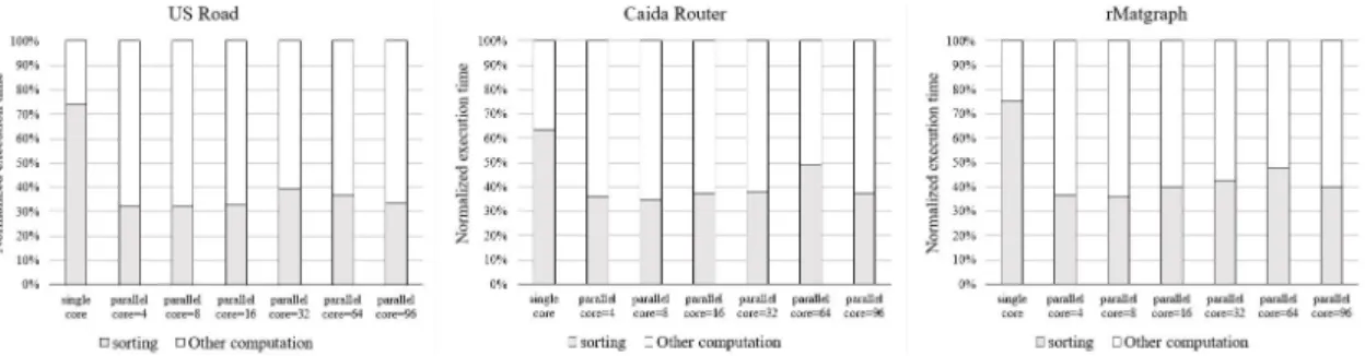
Figure 12. Fractions of graph sort time over total execution time of the serial and parallel MST running on multi-cores.
2.3 Background
2.3.1 Overhead of Sorting in MST
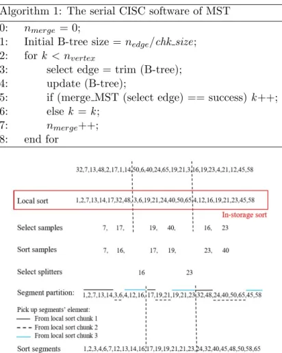
MST computation consists of a number of tasks. The first time-consuming task is edge sorting. To understand how significant the sorting part contributes to the total computation time of MST, we measured the actual sorting time of Kruskal MST and estimated the proportion of sorting time in the entire MST computation. We set up the experiment environment with Intel Xeon processor having 96 cores running at 2.5 GHz. Linux system with kernel version 4.14 was installed on the server. We selected three benchmark datasets from [28∼30]. The parallel software code [9] uses OpenMP when configuring multicores.
Figure 12 shows the breakdown of edge sort time and other computation time of the MST running on 1 to 96 cores. It can be seen from this figure that edge sorting takes a significant proportion of overall MST execution time. For all three benchmarks, we observed consistent behavior. The fraction of time taken for edge sorting ranges from 36% to 75%. In addition to execution time, edge sorting consumes computation resources that could otherwise be used for other computation tasks. Examining the experimental results, we believe such expensive edge preprocessing can be offloaded to data storage device where the large amount of edges is stored.
2.3.2 Previous Work on Near-Data Processing
In many computer systems for the data mining, big-data, and database, the data movement becomes the bottleneck that it causes performance degradation and power waste [34]. Data processing is swiftly moving from computing-centric to data-centric. Inspired by these trends, the concept of NDP [10] (Near-Data Processing) has recently attracted considerable interest: Placing the processing power near the data, rather than shipping the data to the processor. The NDP computation might execute in memory or in the storage device where the input data reside [11], and it can be divided into two main categories: PIM and PIS.
PIM aims at performing computation inside main memory. Various PIM ap-proaches have been proposed since the pioneering work by Gokhale et al. [12]. Recently, Yitbarek et al. [13] have reported accelerator logic for string matching, memory copy, and hash table lookups in hybrid memory cube (HMC) [14][15]. Ahn et al. [16] proposed a scalable PIM architecture for graph processing with five workloads including average teenage follower, conductance, PageRank, single-source shortest path, and vertex cover. They verified the graph processing perfor-mance by simulation.
PIS aims at processing in storage (PIS). Early PIS approaches include the Active Disks architecture proposed by Acharya et al. [17]. They perform the scan, select, and image conversion in storage system and provides a potential reduction of the data movement between disk and CPU. Patterson et al. [18] proposed an architecture (IDISK) which integrates the embedded processors into the disk and push computation closer to the data. Their results suggest that a PIS based architecture can be significantly faster than a high-end symmetric multiprocessing (SMP) based server. Choi et al. [19] implemented algorithms for linear regression, k-means, and string matching in the flash memory controller (FMC). BlueDBM
[20] is a PIS system architecture for distributed computing systems with a flash memory-based FPGA. The authors implemented nearest-neighbor search, graph traversal, and string search algorithms by High-Level Synthesis (HLS) in FPGA. Morpheus [33] frees up scare CPU resources by using embedded processor inside SSD to carry out object deserialization. Recently, Biscuit [21] equipped with FMCs and processes pattern matching logic in storage which speeds up MySQL requests. Lee et al [35] proposed ExtraV, a framework for near storage graph processing such as Average Teenage followers, PageRank, Breadth-First Search and Connected Components. It efficiently utilizes a hardware accelerator at the storage side to achieve performance and flexibility at the same time.
Our focus in this paper is on speeding up graph processing that has become increasingly important in today’s big data era. As will be evidenced shortly, the benefit is great to preprocess a huge amount of graph data inside SSD where the data is stored.
2.4 Hardware Architecture of In-storage Sort 2.4.1 System architecture
The large fraction of time that edge sorting takes in MST and the intelligence available inside modern SSD motivate us to propose a new and practical PIS architecture. Compared with the existing PIS approaches, CISC is unique in that it uses Verilog to generate RTL and provides wire-speed sort in hardware. A pipelined circuit structure was designed to tailor to high-speed storage data sort especially. Graph edge sort is done concurrently with data transfer on the bus. It minimizes sort overhead of the host server CPU which is computation intensive and time-consuming.
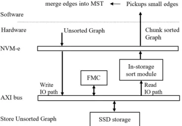
As shown in Figure 13, PIS augments a special functional logic to perform the desired function inside a storage device, in this case, SSD. All the storage control
Figure 13. System architecture of the CISC.
functions are implemented on an FPGA. Inside FPGA chip, major storage logic units include the flash controller, NVM-e interface, DMA engine and in-storage sort module. All modules are connected to AXI4 bus which is a bridge for data movement between host and flash memory. The data width of AXI4 bus is 8 bytes with clock speed of 250MHz. As shown in Figure 13, in-storage sort module is added between AXI bus and NVM-e interface along with storage read I/O path. It provides sort function that is activated by NVM-e command and is done while data is being read from the storage to the host.
2.4.2 In-storage sort module
A challenging problem of hardware sort is to sort the large-scale dataset. Due to the on-chip memory size limitations of FPGA, the existing work [22∼25] par-tially buffers sorted results in the off-chip memory such as DRAM or SSD and reads them back when FPGA performs merge sort. Such off-chip buffer strategy causes multiple FPGA memory accesses and slows down the hardware sort performance of the large-scale dataset.
In order to eliminate the off-chip memory accesses in FPGA sort, CISC takes a divide and conquer approach. Instead of sorting the entire edge list that is huge, we
Figure 14. The architecture of the linear-time sorter.
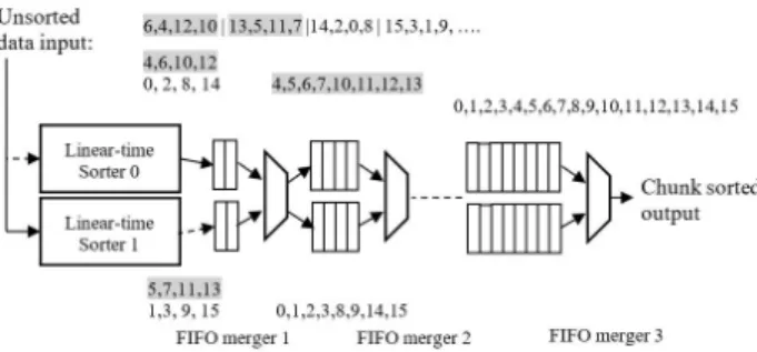
divide the large edge list into chunks and sort these chunks using hardware. Each chunk can fit into FPGA on-chip memory. The pipeline architecture of in-storage sort module provides wire-speed sort of data streams. There are two benefits of dividing edges into chunks to sort. The first one is memory resource savings. It is impossible to hold and reorder large-scale data in FPGA alone. We choose the right chunk size to fit the internal memory space of the FPGA. The second benefit is to bound the in-storage sort latency to match the normal read I/O speed so that the host can read the sorted chunks as if they were directly read from flash memories with no interruption. Once the sorted chunks of edges are loaded to the system RAM, the software on the host can efficiently execute the remaining computation of MST.
The in-storage sort pipeline is composed of the linear-time sorters [25] and several stages of FIFO mergers [22] [24]. We design this architecture especially for the in-storage graph processing with the minimal PIS latency and hardware cost. As the first stage of the pipeline, the linear-time sorter uses n buffers to hold sorted graph edges. It compares each incoming edge’s weight in parallel with all already sorted edges in the buffers and inserts the new graph edge into the appropriate location in the buffers to maintain the existing sorted order [25]. Figure 14 shows an example of n equal to 3 to demonstrate how the linear-time sorter works. Such linear-time sorter generates the sorted sequence ofn edges after
Figure 15. The pipeline architecture of the in-storage sort module.
n clock cycles.
Upon a read I/O from the host, the storage data need to be continuously fed into the PIS function. In order to sort data stream in wire-speed, two linear-time sorters are deployed to work in parallel. As shown in Figure 15, the two linear-time sorters alternate working on the input data and switch functions after every
n clock cycles with one sorting the incoming data stream and the other sending out the sorted results to the next pipeline stage.
The linear-time sorter requires buffers and parallel comparators for the parallel comparisons. Such buffers and comparators will become prohibitive costly if the sorted data size becomes very large. Our solution is again divide and conquer by dividing each chunk of data to be sorted into smaller segments. The dual linear-time sorters only sort the initial segment with a small data size. The in-storage sort module then doubles up such segment by FIFO mergers [24] that form the rest of the pipeline stages as shown in Figure 15. To connect the first pipeline stage (dual linear-time sorters) with the rest of pipeline stages (FIFO mergers), the n sorted edges from the linear-time sorter0 are immediately forwarded to one of the FIFO buffers of the next pipeline stage, FIFO merger1, as shown in Figure 15. During the next n cycles, the linear-time sorter1 fills up the other FIFO buffer of the next pipeline stage. The same process repeats when the storage data continuously flushes into the PIS module.
Each FIFO merger stage doubles up the segment of the previous pipeline stage [24]. For example, the size of data sort doubles up from 4 to 16 when the data stream passes through two stages of the FIFO mergers. As shown in Figure 15, each stage of the FIFO merger has two FIFOs. At any given time, the data stream from the previous pipeline stage flushes to one of the FIFOs. If the flush size reaches the size of the previous segment, a control logic switches the data stream to the other FIFO. After one of the FIFO has finished fetching data with the size of the previous segment, the data merge starts and the fetching data flushes into the other FIFO at the same time. Data in the two FIFOs are merged in ascending order to the next pipeline stage of the FIFO merger, that is, we always pick up the smaller data from two FIFOs to be flushed to the next stage [24]. In this way, the current segment merges two of the previous segments and doubles up the sort size. The sort size of the last segment is the chunk size that depends on the FPGA’s internal resources (numbers of FIFO merger stages). After passing through the in-storage sort module, the graph edges are loaded into the host main memory in form of multiple sorted chunks.
The startup time of such pipeline of FIFO mergers depends on the data trans-fer delay of the last stage of the FIFO merger [24]. The delay is the data transtrans-fer time of the first chunk of the graph data. Therefore, PIS latency is only the pipeline’s startup time when the host server reads the first chunk of a large num-ber of sorted chunks from the storage.
2.5 Software Design of CISC
To allow the MST application to use the in-storage sort module, we developed two CISC software modules running on the host, one for single core CPU and the other for parallel MST running on multicores. The following paragraph describes the software design of CISC.
Figure 16. MST software of CISC on the single-core system.
2.5.1 Serial CISC software
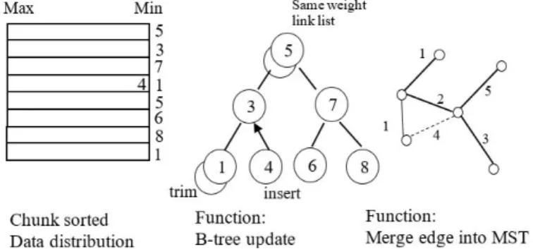
As shown in Figure 16, a B-tree based selection algorithm has been developed in the serial CISC software and coordinates with the chunk sorting circuit. To initialize the B-tree, the serial CISC software picks up graph edges from all the chunk heads. It has nedge/chk size B-tree nodes holding the smallest edges of all
the chunks, where nedge denotes edge numbers and chk size is the chunk size, i.e.
the number of sorted edges per chunk. In order to avoid collision, each B-tree node adds the same weight edges into a linked list. After the initialization of B-tree, the serial CISC software trims the minimum edge from the B-tree by the rule of in-order traversal [26]. A new edge from the chunk head of the trimmed edge is the next B-tree candidate, and the software inserts it into the B-tree after the previous minimum edge is trimmed. The size of the B-tree remains the same (nedge/chk size) during software execution.
As shown in Algorithm 1, the serial CISC software merges the trimmed edges from the B-tree into a graph subset. Once the growing subset forms a cycle, the software abandons the currently selected edge and picks the next edge from the B-tree to grow MST. Such a process stops when MST traverses allnvertex vertices
of the graph, which takes nmerge iterations in Algorithm 1. The B-tree selection
avoids sorting all the graph edges because the smaller edges are placed at the heads of chunks and merge process always picks up the smallest from the B-tree
into MST.
For the same graph, both the software MST and the CISC MST will select the same set of graph edges to form the MST and take same number of iterations,
nmerge, to merge the small edges into the MST. The superiority of serial CISC
MST comes from the graph sort. Instead of sorting nedge edges, the serial CISC
MST picks up a minimum graph edge from the B-tree and merges the graph edge in every iteration. The number of iterations (nmerge) is related tonvertex and much
smaller thannedge in most graphs in practice.
Table 1 shows the time complexities of the sorting part of the MST algorithm of traditional software MST and our CISC. While the best time of software sort is nedge×log2(nedge), CISC sort time is nmerge×log2(nedge/chk size). During the
CISC software execution, the B-tree size remains the same (nedge/chk size). For
B-tree updates, the time complexity is log2(nedge/chk size). Such B-tree update
is performed concurrently with the merge operations of MST. CISC sort finishes when all of the graph vertices (nvertex) are merged, taking nmerge iterations. From
the comparison of these two formulas, we can see CISC takes advantages of both smaller value of nmerge and the efficient data distribution of sorted chunks.
Table 1. Comparison of the serial sort between software and CISC
Execution time of serial sort Software O(nedge×log2(nedge))
CISC O(nmerge×log2(nedge/chk size))
2.5.2 Parallel CISC software
The parallel CISC software cannot use the B-tree selection algorithm because of data dependency. Each edge selection depends on the previous updates of the B-tree, and it may cause task deadlocks wasting the multicores’ computational resources.