ĠSTANBUL TECHNICAL UNIVERSITY INSTITUTE OF SCIENCE AND TECHNOLOGY
M.Sc. Thesis by Fidel BAYAM, B.Sc.
Department: Electronics and Communication Engineering Programme: Electronics Engineering
MAY 2005
CHAOTIC OSCILLATOR BASED RANDOM NUMBER GENERATOR
ĠSTANBUL TECHNICAL UNIVERSITY INSTITUTE OF SCIENCE AND TECHNOLOGY
M.Sc. Thesis by Fidel BAYAM, M.Sc.
(504021207)
Date of submission : 9 May 2005 Date of defence examination: 30 May 2005
Supervisor (Chairman):
Assoc. Prof. Dr. Ali ZEKĠMembers of the Examining Committee Assoc. Prof. Dr. Serdar ÖZOĞUZ
Assist. Prof. Dr. A. ġima ETANER-UYAR
MAY 2005
CHAOTIC OSCILLATOR BASED RANDOM NUMBER GENERATOR
ĠSTANBUL TEKNĠK ÜNĠVERSĠTESĠ FEN BĠLĠMLERĠ ENSTĠTÜSÜ
YÜKSEK LĠSANS TEZĠ Müh. Fidel BAYAM
(504021207)
Tez Danışmanı :
Doç.Dr. Ali ZEKĠDiğer Jüri Üyeleri Doç. Dr. Serdar ÖZOĞUZ
Yrd. Doç. Dr. A. ġima ETANER-UYAR
MAY 2005
KAOTĠK OSĠLATÖR TABANLI RASGELE SAYI ÜRETECĠ
Tezin Enstitüye Verildiği Tarih : 9 Mayıs 2005 Tezin Savunulduğu Tarih : 30 Mayıs 2005
ACKNOWLEDGEMENT
First I would like to thank my supervisor Assoc. Prof. Ali Zeki for his guidance and support during my B.Sc. and M.Sc. thesis.
Next I would like to thank Assoc. Prof. Serdar Özoğuz for his valuable contribution. In this work, the test chip was submitted with the research budget of Assoc. Prof. Dr. Serdar Özoğuz who is awarded by TÜBA‘s (Türkiye Bilimler Akademisi) Young Scientists Award Program (TÜBA-GEBİP).
I feel obliged to thank to my family, without their support, all I could have achieved would be a complete failure.
Finally, I would like to thank Keklik Alptekin for her endless support. I feel very lucky for every single day of six years we have spent together.
CONTENTS
TABLE LIST
vı
FIGURE LIST
vıı
ÖZET
ıx
SUMMARY
x
1. INTRODUCTION 1 1.1 Motivation 1 1.2 Organization of Thesis 12. RANDOM NUMBER GENERATION BASICS 3
2.1 Pseudo Random Number Generators (PRNGs) 4
2.2 True Random Number Generators (TRNGs) 5
2.2.1 SW-Based Generators 5
2.2.2 HW-Based Generators 6
2.3 Post-Processing 6
2.4 Statistical Tests 7
2.4.1 Frequency Test (Monobit Test) 7
2.4.2 Serial Test 7
2.4.3 Poker Test 8
2.4.4 Runs Test 8
2.4.5 Autocorrelation Test 8
2.4.6 FIPS 140-1 Statistical Tests 8
2.5 IC Random Number Generators 9
2.5.1 Direct Amplification of Noise 9
2.5.2 Oscillator Sampling 10
2.5.3 Chaos Based Generators 10
3. CHAOS 12
3.1 Chaos in Electronic Systems 12
3.2 Chua‘s Circuit 14
4. CHAOTIC OSCILLATOR BASED RANDOM NUMBER GENERATOR 16
4.1 Construction of Chaotic Oscillator 16
4.1.1 RLC Resonator 16
4.1.2 Basic LC Oscillator 19
4.1.3 Block Level Chaotic Oscillator 21
4.1.4 Bipolar Transistor Chaotic-LC Oscillator 24
4.1.5 MOS Transistor Chaotic-LC Oscillator 28
4.2 Random Bit Generation 31
4.2.1 Construction of the Clock Signal 33
4.2.2 Combining Bits In One Signal 34
4.2.3 Implementing Von Neumann‘s De-Skewing Algorithm 34
4.3 IC Implementation 35
4.3.1 Bipolar Chaotic Oscillator 36
4.3.2 MOS Transistor Chaotic-LC Oscillator 37
4.3.4 Comparator Circuit 41 4.3.5 ―OR‖ Circuit 42 4.3.6 DFF 44 4.3.7 EXOR Gate 45 4.3.8 Divide-by-two Circuit 46 4.3.9 Output Drivers 47 4.3.10 Toplevel Integration 48 5. CONCLUSION 50 REFERENCES 52 BIOGRAPHY 54
TABLE LIST
Page No
Table 2.1: Conditions of runs test 9
Table 4.1: Different parameter-sets for which chaotic oscillation occurs 23 Table 4.2: Parameter sets that generate chaotic oscillation 30
FIGURE LIST
Page No
Figure 2.1: Direct amplification of noise ... 10
Figure 2.2: Oscillator sampling technique ... 10
Figure 3.1: Chua's Circuit... 14
Figure 3.2: I-V characteristic of Chua's diode ... 15
Figure 3.3: Attractor of Chua's circuit ... 15
Figure 4.1: Parallel RLC circuit ... 16
Figure 4.2: V1 versus t, for R=-10 ... 17
Figure 4.3: V1 versus t, for R=10 ... 18
Figure 4.4: V1 versus t, for R= ... 18
Figure 4.5: The vector field of a system (a) for positive R; (b) for negative R ... 19
Figure 4.6: Implementation of negative resistance with cross coupled transistors .. 20
Figure 4.7: Plot of (V1/VT) for I=1mA, and VT=25mV ... 21
Figure 4.8: Chaotic circuit ... 22
Figure 4.9: V1 for a1=0.6, and a2=2 ... 23
Figure 4.10: Trajectory of the chaotic circuit in Figure 4.8 ... 24
Figure 4.11: Chaotic LC oscillator ... 25
Figure 4.12: Numeric analyses result of the BJT Chaotic-LC oscillator ... 27
Figure 4.13: Trajectory of the BJT Chaotic-LC Oscillator (x versus z) ... 27
Figure 4.14: MOS transistor chaotic-LC oscillator ... 28
Figure 4.15: Waveform of the State Variable x versus time ... 31
Figure 4.16: Trajectory of the MOS Chaotic-LC Oscillator ... 31
Figure 4.17: Constructed subspaces with comparator references ... 32
Figure 4.18: Placement of comparator references ... 33
Figure 4.19: Connections of comparators ... 34
Figure 4.20: construction of clock and data signals ... 34
Figure 4.21: Realization of Von-Neumann‘s De-Skewing Algorithm ... 35
Figure 4.22: Phase Space (VA-VB) versus (VC-VD) of the BJT Chaotic Oscillator .... 37
Figure 4.23: Waveform of (VA-VB) ... 37
Figure 4.24: Phase Space of the MOS Transistor Chaotic Oscillator ... 38
Figure 4.25: Waveforms of (VA-VB) and (VC-VD) differences ... 39
Figure 4.26: Subtraction circuit ... 40
Figure 4.27: DC characteristic of a differential pair ... 40
Figure 4.28: Simulation results of subtraction circuit ... 41
Figure 4.29: Comparator circuit ... 42
Figure 4.30: Simulation results of comp0 and comp1 ... 42
Figure 4.31: OR circuit ... 43
Figure 4.32: Getting Vref ... 43
Figure 4.33: Simulation results of OR circuit ... 44
Figure 4.34: DFF circuit ... 44
Figure 4.35: Simulation results of DFF ... 45
Figure 4.36: EXOR gate ... 46
Figure 4.37: Simulation results of EXOR ... 46
Figure 4.38: Construction of signal "clk/2" ... 47
Figure 4.40: Simulation results of CML drivers ... 48 Figure 4.41: Toplevel layout of the system ... 49
KAOTĠK OSĠLATÖR TABANLI RASGELE SAYI ÜRETECĠ
ÖZET
Bu çalışmada, yüksek hızlı, sürekli zaman LC-kaotik osilatör tasarlanmış ve bu osilatörün çıkışları rasgele bit üretiminde kullanılmıştır. Hem Bipolar hem de MOS transistorlu osilatör versiyonları için devre deklemleri türetilmiştir. Bu denklemlerin nümerik denklem çözücü programlar yardımıyla çözülmesiyle kaotik osilasyonun sağlandığı görülmüştür. Devreler, Spectre spice simülatörü ve IHP SGB25VD 0.25µm SiGeC BiCMOS prosesi model parametreleri kullanılarak test edilmiştir. Rasgele sayı üretimi, osilatör çıkışlarının 2 farklı referansla karşılaştırılmasıyla elde edilmektedir. Oluşturulan bitlerin istatistiksel özelliklerini iyileştirmek amacıyla Von-Neumann algoritması tasarlanarak entegre edilmiştir. Üretilen çıkış bitleri periyodik olmadığından anlamlı bitlerin oluşma anlarını belirten bir saat işareti tanımlanmıştır. Rasgele sayı üretimi için gerekli olan alt bloklar yüksek hızlı çalışmaya uygun olacak şeklide Emetör Bağlamalı Lojik ve Akım Modlu Lojik aileleri kullanılarak tasarlanmıştır. Spectre simülatöründe gerçekleştirilen simülasyonlar, tasarlanan rasgele bit üretecinin yaklaşık 300Mbit/s hızında çıkış oluşturabildiğini göstermiştir. Çıkış işaretlerini cip dışına alabilmek amacıyla Akım Modlu Lojik çıkış sürecüleri tasarlanmıştır. Kaotik osilatör ve rasgele bit üreteci sistemi, IHP SGB25VD 0.25µm SiGeC BiCMOS prosesi ile gerçeklenmiş ve üretime gönderilmiştir. Çipin toplam güç harcaması 50mW mertebesindedir. Toplam kırmık alanı 1 mm x 0.5 mm‘dir.
CHAOTIC OSCILLATOR BASED RANDOM BIT GENERATOR
SUMMARY
In this study, a high speed continuous time LC-chaotic oscillator was designed and utilized as a random bit generator. Circuit equations were derived for both MOS transistor and BJT versions. These equations were solved by using numeric solvers, and chaotic oscillation was observed. Spectre circuit simulator was used as the simulator. Circuits were verified by using IHP‘s SGB25VD 0.25µm SiGeC BiCMOS process. To generate successive ‗1‘s and ‗0‘s, two comparators with different references were used. A well-known Von-Neumann de-skewing algorithm was also implemented in order to improve statistical properties of the generated bit stream. The clock signal was constructed using the outputs of the comparators in order to define the bit generation events. The random bit generation sub-blocks were implemented as bipolar Emitter Coupled Logic (ECL) and Current Mode Logic (CML) gates. Spectre simulations showed that the average throughput of the designed random bit generator is approximately 300Mbit/s. The CML output drivers were designed to output the generated data and clock signals. The whole system, including the BJT chaotic oscillator and the random bit generation sub-blocks, were implemented in IHP‘s SGB25VD 0.25µm SiGeC BiCMOS process. The chaotic oscillator and the random bit generator block consume approximately 50mW power under typical conditions. Total area of the chip is 1 mm x 0.5 mm.
1. INTRODUCTION
1.1 Motivation
Random numbers are statistically independent and unbiased binary digits, and a random number generator is a system whose output consists of fully unpredictable bits. Random Number generation has a great importance in many applications. For example: numerical simulations, gaming, statistical analysis, distributed computations and cryptographic protocols. Almost all cryptographic protocols require the generation and use of secret values that must be unknown to attackers, so in cryptographic applications, the unpredictability of the output implies that the generator must also be not observable and not manipulable by any attacker.
There are two kinds of random number generators (RNGs). Pseudo Random Number Generators (PRNGs) use deterministic algorithms to generate random bits starting from the initial seed. True Random Number Generators (TRGNs) use a non-deterministic phenomenon to produce randomness [1].
True random number generation can be made by using various techniques. One of them is using chaotic circuits. Although chaos is a deterministic process, most times it is accepted to be a true random number generator due to very high initial condition sensitivity and complex behavior. For electronic systems a deterministic system is called chaotic if an infinitesimally small perturbation to its initial conditions produces a change in its behavior.
In 1961, Edward Lorentz discovered the butterfly effect coincidently while trying to forecast the weather. ―Butterfly effect‖ is the idea that very small causes can produce dramatically out-of-proportion effects.
Chaos was first observed electronically in Chua‘s circuit. Chaotic nature of Chua‘s circuit was first observed by Matsumoto in 1983, and the first experimental results of Chua‘s circuit which confirm the presence of chaos were taken by Zhong and Ayrom in 1984 [2].
1.2 Organization of Thesis
This thesis presents a high speed continuous time chaotic-LC oscillator and utilizes it to implement a high speed random bit generator.
Chapter 2 presents basic concepts of random number generation. Different types of random number generators and randomness tests are explained. Important IC implementations are also given.
Chapter 3 is a review of chaos theory.
Chapter 4 is a main subject of the thesis. Designed high speed chaotic LC-oscillator is explained in detail. Random bit generation method is presented in a detail. Implementation of Von-Neumann de-skewing algorithm is also given.
2. RANDOM NUMBER GENERATION BASICS
In general, random numbers can be summarized as numbers that are indistinguishable from outcomes that would arise purely by chance. With another way of saying, random numbers are the statistically independent and unbiased binary digits, that are outputs of algorithmic or device level random bit generators. The quality of a random number generator is often measured by the degree to which it produces unpredictable and unbiased output [2]
Random numbers are widely used in; numerical simulations
gaming
statistical analysis (Monte Carlo simulations) distributed computations,
secure communication protocols (SSL, GSM…) and of course cryptography
Because security protocols rely on the unpredictability of the keys they use, random number generators for cryptographic applications must meet stringent requirements. The most important is that attackers, including those who know the RNG design, must not be able to make any useful predictions about the RNG outputs. In particular, the apparent entropy of the RNG output should be as close as possible to the bit length [1].
According to Shannon theorem, the entropy H of any message or state is:
n i i i p p H 1 log (2.1)where pi is the probability of state i out of n possible states. In the case of a random number generator that produces a k-bit binary result, pi is the probability that an output will equal i, where 0≤i2k. Thus, for a perfect random number generator, pi = 2k and the entropy of the output is equal to k bits. This means that all possible outcomes are equally (un)likely, and on average the information present in the output cannot be represented in a sequence shorter than k bits [1].
Almost all cryptographic protocols require the generation and use of secret number [2]. For example:
Conventional encryption requires the generation of unguessable keys.
The computation of a digital signature with the Digital Signature Algorithm requires, besides the signer's private key, a value customarily called k that must be secret, and that must not be re-used.
Standards for message encryption using the RSA algorithm generally require the use of random numbers to form message padding.
Many challenge-response protocols require the use of a unique number, or nonce. In practice, a good way to produce a number with a large likelihood of being unique is to use a sufficiently large random number.
While a high quality random source is always best, application can be classified into two categories according to randomness requirements [2].
1. Applications which need flat statistic and unbiased bit streams but have fewer unpredictability requirements; such as numerical simulations. In this type of applications pseudo random number generators (PRNGs) can be used
2. Applications which have extremely strong unpredictability requirements but may be slightly tolerant of biased information; such as cryptographic applications. These kind of applications often need true random number generators (tRNG)
2.1 Pseudo Random Number Generators (PRNGs)
In many applications where a random bit stream is required, pseudorandom number generators (PRNGs) are used. Applications where flat statistic and unbiased bits are enough, such as numerical simulations, PRNGs can be safely used. In addition properly-implemented and seeded PRNGs are also suitable for most cryptographic applications, however great care must be taken in the development, testing, and selection of PRNG algorithms. PRNGs use a deterministic process to generate bit sequence, starting from an initial seed. Since the adopted algorithms are usually public, the seed is the only source of randomness and the actual entropy of the output can never exceed the entropy of the seed. Therefore, it is critical that a PRNG be properly seeded from a source of true randomness. In most cases, it must be properly seeded from a source of true randomness.
The output of a PRBG is not random; in fact, the number of possible output sequences is at most a small fraction of all possible binary sequences. The intent is to take a small truly random sequence and expand it to a sequence of much larger length [3].
2.2 True Random Number Generators (TRNGs)
Since it is impossible to create true randomness from within a deterministic system, True Random Number Generators (TRGNs) use a non-deterministic source to produce randomness.
In the applications, the random source can be constructed of dedicated hardware devices; otherwise; the random source can use software procedures to extract random processes from the platform on which the generator is implemented. Generators of the first type are commonly called hardware-based (HW); generators of the second type are software-based (SW) [3].
2.2.1 SW-Based Generators
Generally, SW-based generators are implemented on computer systems and the values typically exploited as raw stream sources are obtained from:
event timings:
o mouse movements and clicks
o keystrokes
o disk and network accesses
data depending on the history of the system and/or large amount of events:
o system clock
o I/O buffers
o Load and network statistics
The behavior of such processes can vary considerably depending on various factors, such as the computer platform, and entropy is mostly low and difficult to evaluate as well as the actual robustness with respect to observation and manipulation.
A well-designed software random bit generator should utilize as many good sources of randomness as are available. Using many sources guards against the possibility of a few of the sources failing, or being observed or manipulated by an adversary. Although employing these protections, it‘s had to say that most PRNGs are immune to attacks. In 1996 two researchers found that Netscape‘s random number
generator seed was derived from ―just three quantities: the time of day, the process ID, and the parent process ID. Thus, an adversary who can predict these three values can apply the well-known MD5 algorithm to compute the exact seed generated [1].
2.2.2 HW-Based Generators
HW-Based generators use a non-deterministic, physical phenomenon to produce randomness. Most operate by measuring unpredictable natural processes. Examples of such physical phenomena include [3]:
1. elapsed time between emission of particles during radioactive decay;
2. thermal noise from a semiconductor diode or resistor;
3. the frequency instability of a free running oscillator;
4. flip-flop metastability
5. the amount a metal-insulator-semiconductor capacitor is charged during a fixed period of time;
6. air turbulence within a sealed disk drive which causes random fluctuations in disk drive sector read latency times; and
7. sound from a microphone or video input from a camera.
2.3 Post-Processing
In practice, every kind of raw random source can present defects as offset, auto-correlation or cross-auto-correlation. The probability of the producing a ‗1‘ bit may not be equal to ½ because of interference with other signals (cross-correlation) or the probability of the generated output bit depends on previous bits because of bandwith limitations (auto-correlation).
There are various techniques for generating truly random bit sequences from the output bits of such a defective generator; such techniques are called de-skewing techniques.
One of the well-known de-skewing algorithms is the Von Neumann‘s algorithm [3]. According to Von Neumann‘s algorithm;
―01‖ sequences must be converted into ‗0‘ bit, ―10‖ sequences must be converted into ‗1‘ bit
―00‖ and ―11‖ sequences must be discarded 2.4 Statistical Tests
Statistical tests are designed to measure the quality of a generator. While it is impossible to give a mathematical proof that a generator is indeed a random bit generator, the tests help detect certain kinds of weaknesses the generator may have. This is accomplished by taking a sample output sequence of the generator and subjecting it to various statistical tests. Each statistical test determines whether the sequence possesses a certain attribute that a truly random sequence would be likely to exhibit; the conclusion of each test is not definite, but rather probabilistic. An example of such an attribute is that the sequence should have roughly the same number of 0‘s as 1‘s. If the sequence is deemed to have failed any one of the statistical tests, the generator may be rejected as being non-random; alternatively, the generator may be subjected to further testing. On the other hand, if the sequence passes all of the statistical tests, the generator is accepted as being random. More precisely, the term ―accepted‖ should be replaced by ―not rejected‖, since passing the tests merely provides probabilistic evidence that the generator produces sequences which have certain characteristics of random sequences. There are 5 basic statistical tests [3].
2.4.1 Frequency Test (Monobit Test)
The purpose of this test is to determine whether the number of ‗0‘bits and in binary sequence (s) of length n are approximately same as would be expected from a random sequence. Let n0, and n1 denote the number of ‗0‘bits and ‗1‘bits in sequence s, respectively. The statistic used is
n n n X 2 1 0 1 (2.2) 2.4.2 Serial TestThe purpose of this test is to determine whether the number of occurrences of 00, 01, 10 and 11 as subsequences of binary sequence s are same, as would be expected for a random sequence. Let n0, and n1 denote the number of ‗0‘bits and ‗1‘bits in s, and let n00, n01, n10, and n11 denotes number of occurrences of ―00‖, ―01‖, ―10‖, and ―11‖ respectively. Note that n00 + n01 + n10 + n11 = (n − 1) since the subsequences are allowed to overlap. The statistic used is
2
1 1 4 2 1 2 0 2 11 2 10 2 01 2 00 2 n n n n n n n n X (2.3)2.4.3 Poker Test
Let m be a positive integer such that
m m n 2 5 and let. m n k . Divide thesequence s into k non-overlapping parts each of length m, and let ni be the number of occurrences of the ith type of sequence of length m, 1i2m. The poker test determines whether the sequences of length m each appear approximately the same number of times in s, as would be expected for a random sequence. The statistic used is k n k X m i i m
2 1 2 3 2 (2.4)The poker test is a generalization of the frequency test: setting m = 1in the poker test yields the frequency test.
2.4.4 Runs Test
The purpose of the runs test is to determine whether the number of runs (of either zeros or ones) of various lengths in the sequence s is as expected for a random sequence. The expected number of gaps (or blocks) of length i in a random sequence of length n is ei
ni3
/2i2. Let k be equal to the largest integer i forwhich. Let Bi, Gi be the number of blocks and gaps, respectively, of length i in s for each i, 1ik. The statistic used is
k i i i i k i i i i e e G e e B X 1 2 1 2 4 ) ( ) ( (2.5) 2.4.5 Autocorrelation TestThe purpose of this test is to check for correlations between the sequence s and (non-cyclic) shifted versions of it.
2.4.6 FIPS 140-1 Statistical Tests
Federal Information Processing Standards (FIPS) specifies four statistical test for randomness with FIPS 140-1 standard [4]:
monobit test. The number n1 of ‗1‘bits in s must satisfy 9654 < n1 < 10346. poker test. The statistic X3 defined by equation (2.4) is computed for m = 4,
and the poker test is passed if 1,03 <X3 < 57,4 is satisfied.
runs test. The number Bi and Gi of blocks and gaps, respectively, of length i in s are counted for each i,1i6 (For the purpose of this test, runs of length greater than 6 are considered to be of length 6). The runs test is
passed if the 12 counts Bi, Gi, 1i6, are each within the corresponding interval specified by the following Table 2.1.
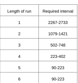
Table 2.1: Conditions of runs test Length of run Required interval
1 2267-2733 2 1079-1421 3 502-748 4 223-402 5 90-223 6 90-223
long run test. The long run test is passed if there are no runs of length 34 or more.
2.5 IC Random Number Generators
The increasing usage and importance of network communication and cryptography results in an increasing to use integrated RNGs. There are a various IC implementations of RNGs, and the important ones are explained below.
2.5.1 Direct Amplification of Noise
The direct amplification technique shown in Figure 2.1 uses a gain high-bandwidth amplifier to process the small ac voltage produced by a noise source such as thermal or shot noise, is in the order of µV making the RNG very sensitive to signal coupling. The noise must be amplified to a level where it can be accurately processed with no bias by a clocked comparator. This is the most popular RNG technique for single-chip solutions where shielding of the noise source is possible. The lack of adequate shielding from power supply and substrate signals in an IC environment prohibits the exclusive use of this method for IC-based cryptographic systems [4].
Figure 2.1: Direct amplification of noise 2.5.2 Oscillator Sampling
Oscillator based RNGs have a advantage over direct amplification of noise technique even in the presence of sinusoidal signal coupling. Oscillator based RNGs use oscillator timing jitter as a source of randomness. Two or more oscillators are combined to produce a random bit stream. In Figure 2.2, a low frequency oscillator samples the output of a high frequency oscillator using a D flip-flop. The level of randomness depends on the mean frequency separation of the oscillators and the amount jitter. If the low frequency oscillator period has a standard deviation much greater than the fast oscillator period, then the states for two successive sampled times can be considered uncorrelated and therefore the output bit stream is random in nature [1].
Figure 2.2: Oscillator sampling technique
In some applications, to improve statistical properties of generated bits, and achive a high bit rates the oscillation frequency of VCO is controlled by other RNG [4].
2.5.3 Chaos Based Generators
A deterministic system is called chaotic if an infinitesimally small perturbation to its initial conditions produces a change in its behavior that grows exponentially with time. Chaos will be examined in detain in the next chapter.
While chaos is a concept completely different from randomness, it is important in random-number generation for the following reason: If an RNG is chaotic, and if there is some inescapable uncertainty in any contribution to its state (e.g., due to thermal noise), then simply by waiting for a certain length of time, namely the time required for the exponential growth of that uncertainty to reach the magnitude of the system's gross state, it can be assumed that the state of the system is unknowable. By waiting a sufficient length of time between samplings, is can be possible to sample high-quality random bits from a chaotic system that is otherwise deterministic [2]. This time period changes from implementation to implementation.
3. CHAOS
The chaos theory is often ascribed to Edward Lorenz. Edward Lorenz was a meteorologist at MIT who showed that weather is chaotic and ultimately unpredictable. In 1961, he used term ―butterfly effect‖ to explain his theory. ―Butterfly effect‖ is the idea that very small causes can produce dramatically out-of-proportion effects. The notion that "the flap of a butterfly's wings in Brazil" might "set off a tornado in Texas" was presented in a lecture by Edward Lorenz to illustrate the impossibility of perfect weather prediction even if all known causes and effects could be measured. The butterfly effect is an illustration of sensitive dependence on initial conditions.
In other way of saying, chaos is the certain systems, in both nature and mathematics, appear to be governed by chance, but can be shown to be deterministic through analysis, phase space maps and computer models. These systems exhibit a sensitive dependence on initial conditions, so that even small variations in their starting conditions will produce wildly differing results.
Every model able to produce chaotic behavior must be a non-linear, dynamical system. Simply, dynamic system is a system in a motion. The swing of a pendulum, boiling water, weather, the growth of populations and the interactions between atoms and molecules are all examples of dynamical systems. Some are predictable and some are not, but they are all systems whose future motions depend entirely on past movements. Dynamical systems signal their presence through three factors:
they are dynamic, that is, subject to lasting changes they are complex, that is, depend on many factors
they are iterative, that is, the laws that govern their behavior can be described by feedback.
Regarding non-linearity, it can be say that systems and phenomena that do not move predictably by following a clear pattern are said to be non-linear.
3.1 Chaos in Electronic Systems
For electronic systems a deterministic system is called chaotic if an infinitesimally small perturbation to its initial conditions produces a change in its behavior that
grows exponentially with time. So, it is impossible to make accurate long-term predictions about the behavior of the system. Chaotic signals are non-periodic in time domain and trajectory of the system cannot go through the same point twice [5]
Chaotic circuits can be used in:
analog signal processing applications as a dither source to improve the performance of other blocks. For instance, dithering can be used to whiten the noise floor of modulators, as well as to reduce the (idle channel) spurious tones, which are introduced during quantization of direct current (dc) inputs (audible in voice-band applications) [6]. Also, dithering can be used to improve the integral nonlinearity of high-performance Nyquist-rate analog-to-digital converters [7].
ranging systems, the nonperiodicity of chaotic signals, as well as the rapid decorrelation of their time-shifted sequences, make the use of chaos an interesting coding technique for high resolution radar systems [8].
chaos-based digital communication systems as a generator of communication carriers [9].
random number generation frequently. Although chaotic oscillator is a deterministic system, most times it is accepted as a TRNG. Since a small changes, affects its behavior, they can be thought as a noise amplificatory.
Chaotic circuits can be classified into autonomous or nonautonomous systems, depending on whether the system is able or not to self-sustain chaotic oscillations without any external excitation. Most of the IC implementations are autonomous systems. Another possible classification is between discrete-time or continuous-time, depending on whether the system evolution is described by nonlinear difference or differential equations, respectively [10].
Autonomous discrete-time systems (or discrete maps) can be generally described by the following qth (delay) order n-dimensional finite-difference equation (FDE),
k
q
F
x
k
q
x
k
x
1
,...,
(3.1)where k=0,1,2… symbolizes the discrete time variable, x(k) represents the state vector of the system at the kth discrete time instant and F is a n-dimensional time-invariant vector field. Autonomous continuous-time systems are defined by the ODE ordinary differential equations (ODE),
)
(
t
x
F
dt
t
dx
(3.2)where x(t) is the state vector of the system (also trajectory) and F is the nonlinear vector field that defines the direction and speed of a trajectory at every point in the state space and at every instant of time [10].
In order to exhibit chaos electronically, an autonomous circuit consisting of resistors, capacitors, and inductors must contain:
at least one nonlinear element (sign, absolute value, hysteresis etc.) at least one negative resistor (to supply energy to the system) at least three energy-storage elements
3.2 Chua’s Circuit
Chua‘s circuit is the simplest electronic circuit that generates chaos [11] (see Figure 3.1).
Figure 3.1: Chua's Circuit It consists of;
A linear inductor L A linear resistor R
Two linear capacitors C1 and C2 and
A single voltage controlled nonlinear resistor called Chua‘s diode. I-V characteristic of Chua‘s Diode is shown in Figure 3.2.
The state equations of Chua‘s circuit are:
(
)
(
)
1
1 1 2 1 1v
f
v
v
G
C
dt
dv
(3.3)
1 2 3
2 2)
(
1
i
v
v
G
C
dt
dv
(3.4) 2 3 1 v L dt di (3.5) where,R
G
1
, andf
v
1
G
bv
1
G
a
G
b
v
1
E
v
1
E
2
1
)
(
.These equations form different attractors for different parameter values. In Figure 3.3 one of the attractors obtained from computer simulation of Chua‘s circuit is shown.
Figure 3.2: I-V characteristic of Chua's diode
4. CHAOTIC OSCILLATOR BASED RANDOM NUMBER GENERATOR
The ultimate goal of this research was to integrate a chaotic oscillator, and use this oscillator outputs to generate a successive bit stream that passes randomness tests. A high speed negative-gm LC oscillator was selected as the oscillator [12]. Random bits were generated with the method described in [13].
By adding new elements to the well known LC oscillator, chaotic oscillation was obtained. The state equations of the oscillator were derived and solved by using various numeric solvers.
4.1 Construction of Chaotic Oscillator
Before substituting equations for the proposed chaotic oscillator, deriving equations for familiar RLC resonator may be helpful in order to illustrate the concepts in dynamical systems theory, and introduce ideas of stability and oscillation,.
4.1.1 RLC Resonator
The parallel-tuned RLC resonant circuit consists of two linear, lossless passive energy-storage elements (L, C) and a linear resistor R (See Figure 4.1).
Figure 4.1: Parallel RLC circuit
This circuit can be described by a system of ordinary differential equations of the form; ), ), ( ( ) (t F X t t X X(0) X0 (4.1)
where X(t) is called a state vector, and F(X(t),t) is called a vector field. If the vector field depends only on the state, and is independent of time t, then the system is said to be autonomous and can be written as [8];
), (X F X X(0) X0 (4.2)
For the circuit in Figure 4.1, with the selection of V1 and iL as state variables, two state equations can be written as;
RC V i C dt dV L 1 1 1 (4.3) L V dt dİL 1 (4.4)
By applying variable transformation as
V
1
x
,
i
L
y
,
andRC t
tn ; the above state equations for the circuit become independent of time t;
x Ry x (4.5) x L RC y (4.6)
Without solving these equations, the behavior of the circuit can easily be explained with respect to the polarity of R. If R is positive then the resistor is said to be dissipative. The energy initially stored in the capacitor and inductor is dissipated, and V1(t) and İL(t) approach zero either monotonically or in the form of exponentially decaying sinusoids. If R is negative, the resistor has negative dissipation; it supplies energy to the rest of the circuit. Energy stored in the circuit increases with time. This circuit simply oscillates when the R infinite.
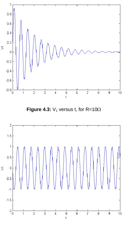
To see the behavior of the circuit visually, equations (4.5) and (4.6) can be solved by using MATLAB. For L=C and a given initial condition-set; the typical voltage V1 waveforms for negative, positive and infinite R situations are shown in Figure 4.2, 4.3, and 4.4 respectively.
Figure 4.3: V1 versus t, for R=10
Figure 4.4: V1 versus t, for R=
The trajectories of a system are also shown in Figure 4.5a,b for positive, and negative R situations respectively (In infinite R situation, the trajectory becomes a simple circle).
Figure 4.5: The vector field of a system (a) for positive R; (b) for negative R For positive R values, trajectories are pushed together as they track spiral towards the origin, which is the equilibrium point of the RLC circuit (Figure 4.5-a). For negative R values trajectories are stretched apart as they track a spiral away from the equilibrium point - the origin (Figure 4.5-b). Although the last situation corresponds to a continuous oscillation, it neither has a physical meaning (A real oscillator must possess a nonlinearity to limit the amplitude of the oscillation), nor is sufficient to produce a chaos.
Indeed, in physical systems there is always a positive R that comes from the parasitic resistance of the inductor. Thus the energy stored in the resonator is dissipated even without the need of an external positive resistor. In order to compensate resonator losses and achieve oscillation, active devices that show negative resistance must be used.
4.1.2 Basic LC Oscillator
Most LC oscillators employ a cross-coupled transistor pair as a negative resistance. Figure 4.6 shows one of the basic configurations of classical LC oscillators. This configuration provides a symmetrical nature to the oscillator.
Since the circuit has a symmetric nature, when node A has a common mode voltage VC and differential voltage +V1, the voltage of node B can be written as VC-V1.
Figure 4.6: Implementation of negative resistance with cross coupled transistors By applying KCL to node A and B, two equations can be written;
0 2 1 1 I e I I dt V d C T C V V V S L (4.7)
0 2 1 1 I e I I dt V d C T C V V V S L (4.8)where IS and VT are the reverse saturation current of the transistor and thermal voltage respectively. By adding, and subtracting (4.7) and (4.8) we conclude with;
)
(
4
2
1
1 1 1 T T T C V V V V V V S Le
e
e
I
i
dt
dV
C
(4.9) ) ( 2 1 1 T T T C V V V V V V S e e I e I (4.10)Rearranging (4.9) by using (3.10) and the tanh definition, one of the state equations of the circuit is reached:
) tanh( 2 2 1 1 1 T L V V I I dt dV C (4.11)
1 2V dt dI L L (4.12) If( 1 ) T V V , and L
I
are chosen as state variables and normalization is applied to time,equations (4.11) and (4.12) can be rearranged with using x V V T ) ( 1 ,
I
y
L
andLC
t
t
n
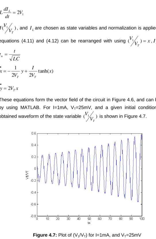
) tanh( 2 2 1 x V I y V x T T (4.13) x V y2 T (4.14)These equations form the vector field of the circuit in Figure 4.6, and can be solved by using MATLAB. For I=1mA, VT=25mV, and a given initial condition-set, the obtained waveform of the state variable ( 1 )
T V
V is shown in Figure 4.7.
Figure 4.7: Plot of (V1/VT) for I=1mA, and VT=25mV
Since there is no amplitude limiting mechanism included, again increasing oscillation is observed.
4.1.3 Block Level Chaotic Oscillator
As discussed in Chapter 3, in order to produce chaos in an electronic system three conditions must be satisfied:
at least one locally active resistor at least three state variables.
By making the appropriate modifications in the circuit seen in Figure 4.6, a sustained chaotic oscillation can be maintained. In Figure 4.8 the new version of the RLC circuit is shown. A resistor (R2) and a capacitor (C2) couple are included in order to produce one more state variable. The Signum function (sgn) is employed as the nonlinear element. It maintains nonlinearity by sourcing a current to node V2 or sinking a current at node V2 according to the polarity of the node voltage V1.
Figure 4.8: Chaotic circuit
For the circuit shown in Figure 4.8, the state equations can be written as;
1 1 1 1
R
V
I
dt
dV
C
L
(4.15) 2 2 1 2 2sgn(
)
R
V
I
V
dt
dV
C
L
(4.16) 2 1 V V dt dI L L (4.17)If V1, RIL, and V2 are chosen as variables, equations (4.15-17) can be rearranged using the variable transformation;
V
1
x
,RI
L
y
,V
2
z
and time normalizationRC t tn . x a y x 1 (4.18) ) ( ) ( 2 z x C L R y (4.19)
z a y x R z sgn( ) 2 (4.20) where 1 1
R
R
a
, and 2 2R
R
a
These equations can be solved by using MATLAB numeric solver ODE45. With the
selection of 1 ) ( 2 C L R
, and L=C, it is seen that chaotic oscillation occurs for some
values of a1, and a2. In Table 4.1, three sets of variables (a1, a2)that provide chaotic oscillation is shown.
Table 4.1: Different parameter-sets for which chaotic oscillation occurs
a1 a2
1 0.6 2
2 0.8 1.6
3 1 1.4
Figure 4.9 shows the waveform of node voltage V1 for the first parameter-set in Table 4.1.
Figure 4.10 is a plot of V1 versus V2, in other words the trajectory of the system in Figure 4.8.
Figure 4.10: Trajectory of the chaotic circuit in Figure 4.8 4.1.4 Bipolar Transistor Chaotic-LC Oscillator
By combining the concepts of classical negative-gm LC oscillator and the circuit that uses the signum function, the final chaotic oscillator has been reached (Figure 4.11) [12]. This circuit has been derived from the classical negative-gm LC oscillator, by adding a parallel RC3 section (like the R2C2 section in Figure 4.8), and a differential pair stage, to realize the signum-like function.
Similar to the classical LC oscillator in Figure 4.6, if node A has a common mode voltage of VC and a differential voltage component of +V1, then node B has a common mode voltage of VC but differential voltage of -V1. Similarly, the voltage values of node C, and D can be written as VC+V2 and VC-V2 respectively, as a result of the symmetrical nature of the circuit.
The inductance, placed between nodes A and C has a current value of
I
L
i
L, whereas the other one hasI
L
i
L.Figure 4.11: Chaotic LC oscillator
Applying KCL at node A, B, C and D, with the assumption of C1=C2=C3=C yields the following equations; 0 ) ( 1 1 L L V V V S C i I e I dt V V d C T C (4.21) 0 ) ( 1 1 L L V V V S C i I e I dt V V d C T C (4.22) 0 ) 2 ( 2 2 2 2 L B L I dt V d C R V I i I (4.23) 0 ) 2 ( 2 2 2 1 L B L I dt V d C R V I i I (4.24)
where IS and VT are the reverse saturation current of the transistor and the thermal voltage respectively.
By rearranging (4.21) and (4.22), the following equations can be written:
T T T C V V V V V V S L e e e I i dt dV C 1 1 2 1 (4.25)
T T T C V V V V V V S L C e e e I I dt dV C 1 1 2 (4.26) By combining (4.23) and (4.24), 4 2 2 1 2 2 i I I R V dt dV C L (4.27)
is achieved. In this equation
I
1
I
2represents the output current difference of the differential pair and can be written in terms of the tail currentI
0 and the differential input voltage as,V
A
V
B
2
V
1.)
tanh(
1 0 2 1 TV
V
I
I
I
(4.28)Equation (4.27) can be rearranged by using (4.28), as
T O LV
V
I
i
R
V
dt
dV
C
2 2 1tanh
4
2
(4.29)Equations (4.25), (4.26) and (4.29) are the state equations of the chaotic oscillator circuit, but there is one more equation that comes from the voltage-current relationship of inductance:
dt i I d L V V V V L L C C ) ( 1 2 (4.30)By making the appropriate simplifications;
dt i d L V V ( L) 2 1 (4.31) is reached.
The 4 equations (4.25, 4.26, 4.29, and 4.31) are the state equations of the circuit shown in Figure 4.11.
By scaling all voltage values with an arbitrary scaling voltage Vs; choosing state variables as S
V
V
x
1 , S LV
R
İ
y
, SV
V
z
2 , and S C CV
V
x
; scaling time t with RC ( RC t tn ); and takingC
L
R
; the state equations are transformed into a simple and dimensionless form:
ax ax
ax e e be y x C 2 (4.32) z x y (4.33)
ax
c
y
z
z
tanh
4
2
(4.34)
ax ax
ax S Ce
e
e
c
c
x
C
2
(4.35) where T S V V a , T S aV R I b , T aV R I c 0 , and T B aV R I I d ) 2 ( 0 .These state equations can be solved by using numeric solvers, and again for different sets of parameters a, b, c and d, chaotic oscillation occurs. Figure 4.12 and 4.13 are obtained for a=0.5, b=10-4, c=8.8 and d=2.
Figure 4.12: Numeric analyses result of the BJT Chaotic-LC oscillator
4.1.5 MOS Transistor Chaotic-LC Oscillator
The MOS transistor version of the chaotic-LC oscillator is also possible (Figure 4.14)
Figure 4.14: MOS transistor chaotic-LC oscillator
Comparing Figure 4.11 and 4.14, it can be seen that transistor type is not the only difference. While currents I1 and I2 are sunk from nodes C and D in Figure 4.11, these currents are sourced to nodes C and D with a gain of k in Figure 4.14.
The nonlinearity in this chaotic oscillator, whose basic structure has been explained in Chapter 4.1.3, has been established by using a transimpedance amplifier block with a signum functionality. While the bipolar differential pair maintains this functionality with a good approximation thanks to the exponential nature of the BJTs, the MOS differential pair cannot achieve a good approximation due to the square-law behavior of MOS transistors. However, it has been seen that in the MOS differential pair, the requested approximation can be achieved when the currents I1 and I2 are multiplied with a gain of k. The circuit structure has been modified accordingly. The currents I1 and I2 could be mirrored once more – this time with NMOS transistors – in order to make a structure, which would be more similar to the BJT version. This modification was not needed.
The currents being sourced this way have made another modification in connections necessary. In the BJT version, the transistor whose base is connected to node A
has its collector at node D, which causes current to be sunk from D according to the voltage value at node A. This connection has been changed in the MOS version and current is being sourced to C according to the voltage value at node A.
Applying KCL at node A, B, C and D, with the assumption of C1=C2=C3=C yields the following equations: 0 ) ( 2 ) ( 2 1 1 L L TN C C i I V V V dt V V d C
(4.36) 0 ) ( 2 ) ( 2 1 1 L L TN C C i I V V V dt V V d C
(4.37) 0 ) 2 ( 2 2 2 2 L B L I dt V d C R V kI i I (4.38) 0 ) 2 ( 2 2 2 1 L B L I dt V d C R V kI i I (4.39) where coupled cross ox n L W C
and VTN is the threshold voltage of the NMOS transistors.By rearranging (4.36) and (4.37), the following equations can be written:
1 1 ) (V V V i dt dV C L
C TN (4.40)
2
1 2 ) ( 2 V V V I dt dV C L C TN C
(4.41) By combining (4.38) and (4.39): ) ( 4 2 1 2 2 2 I I k i R V dt dV C L (4.42)(4.42) is achieved. In equation (4.42) (I1-I2) is the output current difference of the MOS differential pair and by rearranging (4.42) using the output current-input differential voltage relationship of the MOS differential pair, the following equation can be derived:
0 0 2 1 2 1 0 2 22
,
2
4
2
I
I
V
V
V
I
k
i
R
V
dt
dV
C
n n n L
(4.43) Here, pair diff ox n L W C
By scaling all voltage values with an arbitrary scaling voltage Vs; choosing state variables as; S
V
V
x
1 , S LV
R
İ
y
, SV
V
z
2 , and S C CV
V
x
; scaling time t with RC ( RC t tn ); and takingC
L
R
; the state equations are transformed into a simple and dimensionless form:
x c
x b y x C th (4.44) z x y (4.45)
0 0 2 2 02
,
2
4
2
c
b
c
x
x
x
b
c
b
k
y
z
z
n n n
(4.46)
2 2
0 2 x c x b c xC b C th (4.47) whereb
RV
S,b
n
nRV
S S th th V V c , S V R I c 0 0 and S L b V R I c .These state equations again generate chaos for different set of parameters. In Table 4.2, four sets of parameters that generate chaotic oscillation are shown.
Table 4.2: Parameter sets that generate chaotic oscillation b bn cth c0 cb k
1 1 2.6 1 2.2 0.7 1
2 1 0.4 1 0.5 0.7 5
3 1 0.3 1 0.3 0.7 7
4 0.5 0.3 1 0.3 0.7 9
Figure 4.15, and Figure 4.16 show the waveform of the state variable x, and the trajectory of the system (x versus z) respectively for the second parameter set in Table 4.2.
Figure 4.15: Waveform of the State Variable x versus time
Figure 4.16: Trajectory of the MOS Chaotic-LC Oscillator 4.2 Random Bit Generation
The chaotic oscillator presented in the last section, is a continuous time autonomous system, which exhibits a double-scroll attractor. This chaotic oscillator has been used as a source for the RBG.
Bits are produced by using the VA-VB voltage difference which is one of the state variables of the chaotic oscillator. To generate ‗1‘s and ‗0‘s, two comparators with different references are used [13] (Figure 4.17). These two comparators divide the state space into three sub regions; V0, Vtr, and V1. One of the comparators is
responsible for detecting the jumps between the scrolls, and the reference of this comparator has been set to the mid-value of the oscillation. The other comparator is used for detecting the crossings inside one scroll, and the reference of this comparator has been selected as a design variable.
Figure 4.17: Constructed subspaces with comparator references
A ‗1‘ bit is generated when the trajectory passes from region Vtr to region V1 and a ‗0‘ bit is generated when the trajectory passes from region Vtr to region V0.
The time domain representation of the reference placement is shown in Figure 4.18. In Figure 4.18, the x-axis is the voltage signal (VA-VB), which is one of the state variables of the system described in section 4.1.4
It is easy to see that by using the bit generation procedure that has just been explained, and applying the comparator references as seen in Figure 4.18, the resulting number of ‗1‘s will be significantly less than that of ‗0‘s. This nonsymmetrical replacement of references can be overcome by a proper selection of the reference of comp0 (ref0), and applying Von-Neumann de-skewing algorithm as explained in chapter 2.
Figure 4.18: Placement of comparator references
Up to here, the ‗1‘s have been generated at the output of the comparator comp1 at 0 to 1 crossings, and ‗0‘s at the output of comparator comp0 at 1 to 0 crossings. It is obvious that this is not an appropriate way of outputting random numbers, therefore another method should be found.
4.2.1 Construction of the Clock Signal
In data transport protocols, it is common to synchronize the data on the line with a synchronization signal, namely the clock. Therefore combining the generated ‗1‘s and ‗0‘s in one signal and defining a clock signal would be a better way of outputting random bits.
The clock signal must point to the meaningful bits. As a result, it has to be constructed using the comparator outputs.
The first step of clock generation is to make the two comparators similar in the way they generate ‗1‘s and ‗0‘s. In order to achieve that, the reference and signal inputs of comp0 have been interchanged. Thus comp0 generates ‗0‘s during 0 to 1 crosses; while comp1 keeps generating ‗1‘s during 0 to 1 crossings.
Figure 4.19: Connections of comparators
This new arrangement gives us an opportunity to combine the two comparator outputs by using an OR function. The output of this OR function is the clock signal that we need.
4.2.2 Combining Bits In One Signal
Since the two comparators are taking the same signal as input and reference of comp0 is smaller than comp1; the output of comp1 has already been set to ‗0‘ whenever comp0 produces ‗0‘. This means that sampling the output of comp1 with the constructed clock signal gives us the random bit stream that has been generated by system the (Figure 4.20).
Figure 4.20: construction of clock and data signals 4.2.3 Implementing Von Neumann’s De-Skewing Algorithm
As explained in chapter 2, generated bits may have cross or auto correlation related defects. For example, if the reference of comp0 is selected improperly, the resulting number of ‗0‘s would be significantly higher that that of ‗1‘s. De-skewing can be applied to the generated bits to prevent correlation related defects. Von Neumann‘s well known de-skewing algorithm was implemented to improve the statistical properties of the produced bits. With this de-skewing algorithm ―01‖ sequences are converted into ―0‖; ―10‖ sequences are converted into ―1‖; ―00‖ and ―11‖ sequences are discarded.
Although this de-skewing would change the generated bit sequences, since the meaningful bits have been defined by the generated clock signal, the manipulations to implement Von Neumann‘s de-skewing algorithm must be applied to the clock
signal. The complete block level diagram, where de-skewing algorithm is realized, is shown in Figure 4.21.
Figure 4.21: Realization of Von-Neumann‘s De-Skewing Algorithm In figure 4.21:
Data signals have been stored into two consecutive DFFs (DFF1, DFF2). To eliminate the ―00‖s and ―11‖s and keep the ―01‖s and ―10‖s, the outputs of
these two DFFs have been EXORed.
To process the non-overlapping bit pairs only, the clock signal has been divided by two again using DFF (DFF4).
To get the final clock signal (clk_out), outputs of EXOR and DFF4 have been combined by using AND function. If the EXOR operation results ―0‖, the signal ―clk/2‖ is disabled by this AND gate.
DFF5 has been used to synchronize the data signal with the newly constructed clock signal, and it produces the final data.
4.3 IC Implementation
In the first steps of the design process, AustriaMicroSystems (AMS) 0.35m SiGe BiCMOS process had been chosen for production and the oscillator circuits had been designed and simulated by using the parameters of this process. Afterwards, out of financial reasons, the process to be used was changed to the IHP 0.25m SiGe-C BiCMOS process, and the design was completed in this process and sent along for production.
It was proven numerically in section 4.1 that the designed oscillators can generate chaotic oscillation. By choosing an appropriate parameter-set out of the sets that
generate chaotic oscillation and using the definitions of these parameters, the values of the circuit elements have been identified. Although different sets of parameters produce chaos in numeric analyses, some parameter sets are not meaningful in physical basis. In other words, not all of the parameter sets that numerically generate chaos can produce suitable L, C and R values for IC implementation.
With the existence of transistors with high transit frequency, the RBG blocks were implemented using standard ECL and CML structures.
Cadence Spectre circuit simulator was used as the simulator. Supply voltages were 1.2V. Simulations have been verified for various corner parameters, and temperature was swept from -20 0C to 50 0C.
4.3.1 Bipolar Chaotic Oscillator
R, L, C, IB, and I0 were calculated for the parameter values a=0.5, b=10-4, c=8.8, and d=2. With using definitions of these four parameters
-T S V V a , T S aV R I b , T aV R I c 0 , and T B aV R I I d ) 2 ( 0
- and choosing L=11.7nH we conclude with the other element values as R=180, C=350fF, and DC bias currents I0=600A, IB=710A.
L=11.7nH was chosen to be able to use standard inductances supplied by the vendor. By doing this, we can avoid design and layout of inductances customly. Since, these parameters do not restrict the selection of transistor geometries, transistor geometries were determined in such a way that maximum transit frequency and current gain occur for the transistors at given current levels.
After first simulations:
IB was changed to 800A
C values were reduced in order to compensate parasitic capacitances at node A,B,C and D
In contrast to the differential pair, the cross coupled stage transistors were changed with large area ones, to be able to reduce the base resistance which was not included in the state equations
Figure 4.22 and 4.23 show the observed phase space corresponding to (VA-VB) versus (VC-VD) and time domain waveform of (VA-VB) respectively.