ANFIS Controller based Voltage Controlled DSTATCOM Using
External Inductor
𝑺. 𝑲. 𝑺𝒂𝒎𝒆𝒆𝒓𝟏, PG Scholar, Department of EEE, SHREE Institut e o f T ech n ical Educat io n , Go p alap ur am , T ir up at i, A.P , I n dia
𝒀. 𝑷𝒆𝒓𝒂𝒊𝒂𝒉𝟐, M.Tech (PE), Department of EEE, SHREE Instit ut e o f T ech n ical Educat io n , Go p alap ur am , T ir up at i, A.P , I n dia
ABST RACT—this project proposes the Design of External In duct o r f or Improving Performance of DST ATCOM with ANFIS f o r bet t er Vo ltage regulation & harmonic reduction. A DST ACOM is used f o r lo ad voltage regulation and its performance mostly is contingent upo n t he feeder impedance and its nature (resistive, inductiv e, st if f , n o n st iff). On the other hand, a study for investigating voltage regulat io n p erformance of DSTATCOM with ANFIS depending upon n et wo r k p arameters is not well defin ed. T h is p ap er aim s t o p r o v ide a comprehensive study of design, operation, and flexible ANFIS control o f a DSTATCOM operating in voltage cont r o l m o de. A det ailed an alysis of the voltage regulation capability of DSTAT COM un de r v arious feeder impedances is presented. Then, a ben ch m ar k design p rocedure to compute the value of external inductor is pr esen t ed. A dy namic reference load voltage generation scheme is also develo p ed, wh ich allows DST ATCOM to compensate load reactive power durin g n ormal operation, in addition to providing volt age sup p o r t dur in g disturbances. Simulation results validate the eff ect iv e n ess o f t h e p r o p o sed ANFI S sch em e.
I n dex Terms—Distribution static compensator (DSTATCOM), power f actor, power quality (PQ), voltage co n t r o l, ANFI S co n t r o ller .
I. I NT RODUCT I ON
Large electric drives and utility applications require advanced power electronics converter to meet the high power demands. T he evolution of power electronic devices, nonlinear loads, and unbalanced loads has degraded the power quality in the power distribution network. The distribution static compensator is a shunt active filter, which injects currents into the point of common coupling (PCC) (the common point where load, source, and DST AT COM are connected) such that the harmonic filtering, power factor correction, and load balancing can be achieved. In practice, the presence of feeder impedance and nonlinear loads distorts the terminal voltage (PCC) and source currents. The load compensation using state feedback control of DST AT COM with shunt filter capacitor gives better results. T he switching frequency components in the terminal voltages and source currents are eliminated by using state feedback control of shunt filter capacitor. In this situation, DST AT COM should operate in CCM. However, due to grid faults, source voltage (stiff or non-stiff) can change at any time and then VCM operation is required. DST AT COM regulates the load voltage by indirectly regulating the voltage across the feeder impedance. When a load is connected to nearly a stiff source, feeder impedance will be negligible. Faults in a widespread power system as well as switching of sizably voluminous loads engender voltage perturbances such as sag and swell in a distribution system. These power quality (PQ) quandaries significantly degrade the performance of sensitive loads like process-control industry, electronics equipment, adjustable drives, etc.
Power quality is one of the most consequential aspects concerned by utility and residential customer, especially when it becomes a very sensitive issue for industrial consumer. Power quality betokens the faculty to receive pristine electrical voltage sinusoidal waveform at distribution point. It is conspicuous that everyone will aim to gain the excellent quality in every situation no matter in which aspect, and power quality should not be omitted. Power quality quandaries are not incipient issues in a electrical power system and every electrical utilizer might want to minimize their effect on electrical equipment so that the highest possible power quality could be obtained by all of the users.
T he transmutations of the voltage supplied even for very short period of time, which were not authentically mostly taken attention by public, is now very sumptuous due to their cause of infelicitous operation and shut down situation in manufacturing plants. For the purport of getting the highest efficiency in engenderment besides for sustaining of the most plausible operating cost, electrical customers were now agog for the high power quality. For instance, perturbances like voltage sag, which was introduced by the higher fault on the network, will influence more number of customer victims. Ergo, an opportune study and tenaciousness about the puissance quality perturbances should be conducted solemnly as well as the extenuation manners not only to consummate customers demand, but withal increase the reputation and quality of electrical power in our country.
In order to further understand the sophisticated power quality quandaries, the recordings of all perturbances are now done by installing the on-line power quality monitoring system. Besides that, sundry professional surveys had conducted in date. Hence, it is conspicuously that power quality perturbances are now became the very crucial topic for us to understand and study more. It signifies that the detection and mitigation of voltage sag in electrical power system are withal very paramount to achieve amelioration in power system so that their benefits could be experienced by people in whole country.
Conventionally, static var compensator (SVC) is utilized to regulate load voltage, compensate reactive current, and amend transient stability. However, the SVC causes quandaries like harmonic current injection in the system, harmonic amplification, and possible resonance with the source impedance. Distribution static compensator (DST AT COM) has been proposed to surmount the inhibitions of SVC [3]–[9]. A DST AT COM is one of the most efficacious solutions to regulate the load voltage. It provides load voltage regulation by supplying fundamental reactive current into source.
However, most of the conventional DST AT COMs utilized for voltage regulation consider highly inductive and/or significantly astronomically immense feeder impedance. T his is conventionally erroneous in a distribution system where feeder impedance used to be resistive in nature. In this scenario, the DST AT COM will have diminutive voltage regulation capability. Another consequential is-sue is the generation of reference load voltage. In conventional DST AT COM application for voltage regulation, reference load voltage is set at 1.0 per unit (p.u.). At this load voltage, voltage-source inverter (VSI) always exchanges reactive power with the source with leading power factor. This causes continuous power losses in the feeder and VSI. Additionally, a conventional DST ATCOM requires high-current rating VSI to provide voltage support. T his high-current requisite increases the potency rating of the VSI and engenders more losses in the switches as well as in the feeder.
T he voltage regulation performance of DST AT COM mainly depends upon the feeder impedance and its nature (resistive, inductive, stiff, and nonstiff). For voltage control mode (VCM) operation of DST AT COM and/or grid-connected inverters, the conception of inserting an external inductor in line has been reported. However, in these schemes, only the concept has been introduced leaving ample scope for further investigation and insight into the design details.
T he focus of this paper is to provide a detailed design procedure for culling the external inductor which satiates several practical constraints, sanction DSTATCOM to regulate load voltage in stiff as well as resistive feeder, reduce the current requisite for mitigation of sag, and reduce the system losses. With coordinated control of the load fundamental current, terminal voltage, and voltage across the external inductor, a dynamic reference load voltage generation scheme is presented. T his scheme ascertains unity power factor (UPF) operation during mundane operation and maintains load voltage constant during voltage perturbances. Detailed simulation and experimental results are included to verify the DST AT COM performance.
I I . DST ATCOM IN THE POW E R DI ST RI BUT I ON SYST E M
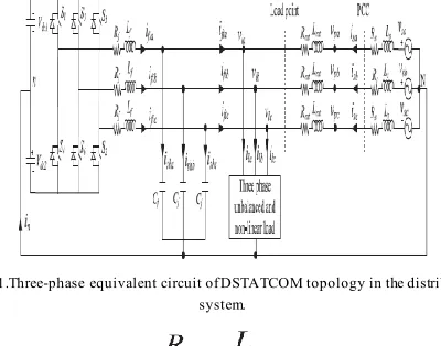
Fig. 1 shows the power circuit diagram of the DST AT COM topology connected in the distribution system. Ls and Rs are source inductance and resistance, respectively. An external inductance Lext is included in
series between load and source points. T his inductor helps DST AT COM to achieve load voltage regulation capability even in worst grid conditions, i.e., resistive or stiff grid. From IEEE-519 standard, point of commoncoupling (PCC) should be the point which is accessible to both the utility and the customer for direct measurement [20]. T herefore, the PCC is the point where Lext is connected to the source. T he DST AT COM is connected at the point where load and
Lext are connected. T he DST AT COM uses a three-phase four-wire VSI. A passive LC filter is connected in each phase to filter out high-frequency switching components. Voltages across dc capacitors, Vdc1 and Vdc2 , are maintained at a reference value of Vdcref.
Fig. 1.Three-phase equivalent circuit of DSTATCOM topology in the distribution system.
Fig. 2.Equivalent source-load model without considering external inductor.
I I I . E FFE CT OF FE E DE R I MP E DANCE ON VOL T AGE RE GUL AT I ON
T o demonstrate the effect of feeder impedance on voltage regulation performance, an equivalent source-load model without considering external inductor is shown in Fig. 2. The current in the circuit is given as
where V s = Vs∠δ, V l = Vl∠0, I s = Is∠φ, andZs= Zs∠θs, with Vs, Vl, Is , Zs, δ, φ, and θsare rms source voltage, rms load voltage, rms source current, feeder impedance, load angle, power factor angle, and feeder impedance angle, respectively. T he three-phase average load power (Pl) is expressed as
Substituting V l and I sinto (2), the load active power is
For power transfer from source to load with stable operation in an inductive feeder, δmust be positive and less than 90◦. Also, all the terms of the second part of (4), i.e., inside cos−1, are amplitude and will always be positive. Therefore, the value of the second part will be between “0” and “π/2” for the entire operation of the load. Consequently, the load angle will lie between θsand (θs − π/2) under any load operation, and therefore, maximum possible load angle is θs. T he vector expression for source voltage is given as follows:
Vs= Vl+ IsZs∠(θs+ φ) . (5)
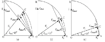
A DST AT COM regulates the load voltage by injecting fundamental reactive current. T o demonstrate the DST ATCOM voltage regulation capability at different supply voltages for different Rs/Xs, vector diagrams using (5) are drawn in Fig. 3. T o draw these diagrams, load voltage Vlis taken as reference phasor having the nominal valueOA(1.0 p.u.).With aim of making Vl= Vs= 1.0 p.u., locus of Vswill be a semicircle of radius Vl. Since the maximum possible load angle is 90◦ in an inductive feeder, phasorVscan be anywhere inside curve OACBO. It can be seen that the value of θs+ φmust be greater than 90◦ for zero voltage regulation. Additionally, it is possible only when power factor is leading at the load terminal as θscannot be more than 90◦.
Fig. 3. Voltage regulation performance curve of DSTATCOM at different Rs/Xs. (a) For Rs/Xs= 1. (b) For Rs/Xs=√3. (c) For Rs/Xs= 3.73
Fig. 3(a) shows the limiting case when Rs/Xs= 1, i.e., θs= 45◦. From (4), the maximum possible load angle is 45◦. T he maximum value of angle, θs+ φ, can be 135◦ when φis 90◦. Hence, the limiting source current phasorOE, which is denoted by Islimit, will lead the load voltage by 90◦. Lines OC and AB show the limiting vectors of Vsand IsZs, respectively, withDas the intersection point. Hence, area under ACDA shows the operating region of DST AT COM for voltage regulation. The point D has a limiting value of Vslimit = IsZs= 0.706 p.u. T herefore, maximum possible voltage regulation is 29.4%. However, it is impossible to achieve these two limits simultaneously as δand φcannot be maximum at the same time. Again if Zsis low, the source current, which will be almost inductive, will be enough to be realized by the DST AT COM.
Fig. 3(b) considers case when Rs/Xs=√3, i.e., θs= 30◦. T he area under ACDA shrinks, which shows that with the increase in Rs/Xs from the limiting value, the voltage regulation capability decreases. In this case, the limiting values of Vs limit and IsZs are found to be 0.866 and 0.5 p.u., respectively. Here, maximum possible voltage regulation is 13.4%.However, due to high-current requirement; a practical DST AT COM can provide very small voltage regulation.
Voltage regulation performance curves for more resistive grid, i.e., θs=15◦, as shown in Fig. 3(c), can be drawn similarly. Here, area underACDAis negligible. For this case, hardly any voltage regulation is possible. T herefore, more the feeder is resistive in nature,
lesser will be the voltage regulation capability. T herefore, it is inferred that the voltage regulation capability of DST ATCOM in a distribution system mainly depends upon the feeder impedance. Due to resistive nature of feeder in a distribution system, DST AT COM voltage regulation capability is limited. Moreover, very high current is required to mitigate small voltage disturbances, which results in higher rating of insulated-gate bipolar transistor switches as well as increased losses. One more point worth to be noted is that, in the resistive feeder, there will be some voltage drop in the line at nominal source voltage which the DST ATCOM may not be able compensate to maintain load voltage at 1.0 p.u. even with an ideal VSI.
I V. SELECTION OF EXTERNAL INDUCTOR FOR VOL T AGE RE GULATION IMPROVEMENT AND RAT I NG RE DUCT I ON
T his section presents a generalized procedure to select external inductor for improvement in DST AT COM voltage regulation capability while reducing the current rating of VSI. Fig. 4 shows single-phase equivalent DST AT COM circuit diagram in distribution system.With balanced voltages, source current will be
whereRsef = Rs+ Rext and Xsef = Xs+ Xext are effective feeder resistance and reactance, respectively. Rext is equivalent series resistance (ESR) of external inductor, and will be small. With θsef = tan−1 XsefRsef and Zsef = _ R2 sef + X2 sef as effective impedance angle and effective feeder impedance, respectively, the imaginary component of I sis given as
With the addition of external impedance, the effective feeder impedance becomes predominantly inductive. Hence, Zsef≈ Xsef. T herefore, approximated Iim s will be
DST AT COM Power rating (Svsi) is given as follows [21]:
Where Ivsi is the rms phase current rating of the VSI and Vdc is the voltage maintained at the dc capacitors. T he DST AT COM aims to inject harmonic and reactive current component of load currents. Suppose Iim l is the maximum rms reactive and harmonic current rating of the load; then, the value of compensator current used for voltage regulation (same as Iims ) is obtained by subtracting Iim l from Ivsi and given as follows:
T he above expression is used to compute the value of external inductor. A design example of external inductor, used for this study, is given in the next section.
V. DE SI GN E XAMP L E OF E XT E RNAL I NDUCT OR
Here, it is assumed that the considered DST AT COM pro-tects load from a voltage sag of 60%. Hence, source voltage Vs=0.6 p.u. is considered as worst case voltage disturbances.During voltage disturbances, the loads should remain operational while improving the DST AT COM capability to mitigate the sag. T herefore, the load voltage during voltage sag is maintained at 0.9 p.u., which is sufficient for satisfactory operation of the load. In the present case, maximum required value of Ilimis 10 A. With the system parameters given inTable I, the effective reactance after solving (11) is found to be 2.2 Ω (Lsef =
7 mH). Hence, value of external inductance, Lext, will be 6.7 mH.
T his external inductor is selected while satisfying the constraints such as maximum load power demand, rating of DST AT COM, and amount of sag to be mitigated. In this design example, for base voltage and base power rating of 400 V and 10 kVA, respectively, the value of external inductance is 0.13 p.u. Moreover, with a total inductance of 7 mH (external and actual grid inductance), the total impedance will be 0.137 p. u. T he short-circuit capacity of the line will be 1/0.13 = 7.7 p.u., which is sufficient for the satisfactory operation of the system. Additionally, a designer always has flexibility to find suitable value of Lext if the constraints are modified or circuit
conditions are changed. Moreover, the conventional DST AT COM operated for achieving voltage regulation uses large feeder inductances [11], [13].
T ABLE I
SIMULAT ION PARAMET ERS
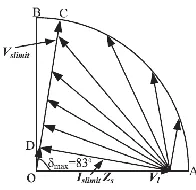
With the external inductance while neglecting its ESR, Rs
/Xsef will be 0.13, i.e.,θsef= 83◦. Voltage regulation performance curves
of the DST AT COM in this case are shown in Fig. 5, of the stable operating range OABO. Hence, introduction of external inductor greatly improves the DST AT COM voltage regulation capability. Additionally, due to increased effective feeder impedance, the current requirement for sag mitigation also reduces. Moreover, if ESR of the external inductor is included, then the equivalent feeder impedance angle changes slightly (i.e., from 83◦ to 80.45◦) and has negligible effect on the expression obtained in (11) as well as the voltage regulation capability of the DST AT COM.
Fig. 4.Voltage regulation performance of DSTATCOM with external inductance.
VI . DESIGN OF ADAPT IVE NEURO -FUZ Z Y CONT ROLLER
Adaptive neuro fuzzy inference system (ANFIS) integrates the best features of fuzzy systems and neural networks, and it has potential to capture the benefits of both in a single frame work. ANFIS is a kind of artificial neural network that is based on T akagi-sugeno fuzzy inference system, which is having one input an done output. Using a given data set, the toolbox function of ANFIS constructs a fuzzy inference system (FIS) where as the membership function parameters are tuned (adjusted) using a back propagation algorithm. In order to have an idea of optimized ANFIS architecture for proposed control, an initial data is generated from normal PI regulator and the data is saved in workspace of MATLAB. T hen the ANFIS command window is opened by typing anfis editor in the main MAT LAB window. T hen the data previously saved in workspace is loaded in the ANFIS command window to generate an optimized ANFIS architecture as shown in Fig.3.
Figure. 4(a) Optimized ANFIS architecture suggested by MATLAB/anfiseditor.
In Fig.4 shows schematic of the proposed ANFIS based control architecture. T he node functions of each layer in the ANFIS architecture are described as follows:
T he error between reference link voltage and actual dc-link voltage (ξ=Vdc*-Vdc) is given to the neuro-fuzzy controller and the
same error is used to tune the precondition and consequent parameters [10]. T he control of dc-link voltage gives the active power current component (id *’), which is further modified to take in account of
active current component injected from RES (iRen).The node functions
of each layer in ANFIS architecture are as described below:
Layer 1: T his layer is also known as fuzzification layer where each node is represented by square. Here, three membership functions are assigned to each input. T he trapezoidal and triangular membership functions are used to reduce the computation burden as shown in Fig. 5. And the corresponding node equations are as given below:
𝜇𝐴1(𝜀) =
1 𝜀 ≤ 𝑏1 𝜀−𝑎1
𝑏1−𝑎1 𝑏1 < 𝜀 < 𝑎1
0 𝜀 ≥ 𝑎1
}
𝜇𝐴2(𝜀) =
1 −𝜀−𝑎1
0.5 𝑏2 |𝜀 − 𝑎2| ≤ 0.5𝑏2
0 |𝜀 − 𝑎2| ≥ 0.5𝑏2
}
𝜇𝐴3(𝜀) =
0 𝜀 ≤ 𝑎3
𝜀 − 𝑎1
𝑏1− 𝑎1
𝑎3< 𝜀 < 𝑏3
1 𝜀 ≥ 𝑏3
} (12)
where the value of parameters (ai, bi) changes with the change in error
and accordingly generates the linguistic value of each membership function. Parameters in this layer are referred as premise parameters or precondition parameters.
Figur e. ( 6 a) Fuzzy m em ber sh ip f un ct io n s.
Layer 2: Every node in this layer is a circle labelled as Π. which multiplies the incoming signals and forwards it to next layer
𝜇𝑖= 𝜇𝐴𝑖(𝜀1).𝜇𝐵𝑖(𝜀2) … …i=1,2,3,… But in our case there is only one input, so this layer can be ignored and the output of first layer will directly pass to the third layer. Here, the output of each node represents the firing strength of a rule.
Layer 3: Every node in this layer is represented as circle. T his layer calculates the normalized firing strength of each rule as given below:
̅̅̅ 𝜇𝑖= 𝜇𝑖
𝜇1+𝜇2+𝜇3 (13)
Layer 4: Every node in this layer is a node function
𝑂𝑖= 𝜇̅𝑖 .𝑓𝑖= 𝜇̅𝑖(𝑎0𝑖+ 𝑎1𝑖𝜀) i=1,2,3.
where the parameters (𝑎0𝑖,𝑎 1
𝑖 )are tuned as the function of input (ξ). T he parameters inthis layer are also referred as consequent parameters.
Layer 5: T his layer is also called output layer which computes the output as given below: T he output from this layer is multiplied with the normalizing factor to obtain the active power current component.
Fig. 6. Block diagram of the proposed flexible control strategy.
T he reference source currents must be in phase with the respective fundamental positive-sequence PCC voltages for achieving UPF at the PCC. Instantaneous PCC voltage and reference source current in phase-a can be defined as follows:
whereV + pa1 and ϕ+ pa1 are rms voltage and angle of fundamental positive-sequence voltage in phase-a, respectively. I∗sais the rms reference source current obtained from (12). With external impedance, the expected load voltage is given as follows:
From (15) and (16), the load voltage magnitude will be
With UPF at the PCC, the voltage across the external inductor will lead the PCC voltage by 90◦. Neglecting ESR of external inductor, it can be observed that the voltage across external inductor improves the load voltage compared to the PCC voltage.
T his highlights another advantage of external inductor where it helps in improving the load voltage. As long as Vlalies between 0.9 and 1.1 p.u., same voltage is used as reference terminal voltage (V ∗ l ), i.e.,
2) Operation During Sag: Voltage sag is considered when value of (18) is less than 0.9 p.u. T o keep filter current minimum, the reference voltage is set to 0.9 p.u. T herefore,
3) Operation During Swell: A voltage swell is considered when any of the PCC phase voltage exceeds 1.1 p.u. In this case, reference load voltage (V ∗ l ) is set to 1.1 p.u., which results in minimum current injection. T herefore,
Average real power at the PCC (Ppcc) is sum of average load power (Pl ) and VSI losses (Ploss). T he real power Ppcc is taken from the source depending upon the angle between source and load voltages, i.e., load angle δ. If DST AT COM dc bus capacitor voltage is regulated to a reference value, then in steady-state condition, Ploss is a constant value and forms a fraction of Ppcc. Consequently, δis also a constant value.
T he dc-link voltage is regulated by generating a suitable value of δ. T he average voltage across dc capacitors (Vdc1 + Vdc2) is compared with a reference voltage and error is passed through a PI controller. Output of PI controller, δ, is given as
Wherevdc = 2Vdcref − (Vdc1 + Vdc2 ) is the voltage error. Kpδ and Kiδ are proportional and integral gains, respectively.
C. Generation of Instantaneous Reference Voltage
Selecting suitable reference load voltage magnitude and computing load angle δfrom (21), the three-phase balanced sinusoidal reference load voltages are given as follows:
T hese voltages are realized by the VSI using a predictive voltage controller [23].
VI I . MAT L AB/SI MUL I NK RE SUL T S
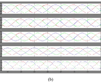
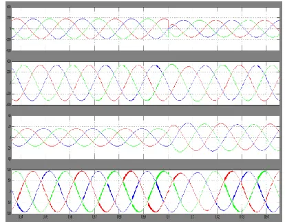
T he control scheme is implemented using PSCAD software. Simulation parameters are given in T able I. fig 7(a) show the MAT LAB/SIMULINK Model of the Proposed ANFIS based DST AT COM. Fig. 7(b) shows the T erminal voltages and source currents before compensation are plotted. Distorted and unbalanced source currents flowing through the feeder make terminal voltages unbalanced and distorted. T hree conditions, namely, nominal operation, operation during sag, and operation during load change are compared between the traditional and proposed method. In the traditional method, the reference voltage is 1.0 p.u. whereas in the proposed method used to find the reference voltage.
Fig 7(a)
(b)
Fig. 7(a) Simulink model of the proposed ANFIS based DSTATCOM (b) PCC voltages, Load Voltages, Source currents & Filter Currents Load Currents using
the traditional method.
A. Nominal Operation
Initially, the traditional method is considered. Fig. 7(b),(a)– (c) shows the regulated terminal voltages and corresponding source currents in phases. T hese waveforms are balanced and sinusoidal. However, source currents lead respective terminal voltages which show that the compensator supplies reactive current to the source to overcome feeder drop, in addition to supplying load reactive and harmonic currents. Fig. 9
Fig 8 Reactive power of the Load , PCC & DSATCOM
Fig. 9. (a) Voltage at the dc bus.
at the load terminal. For the considered system, waveforms of load reactive power ( Ql), compensator reactive power ( Qc), and reactive power at the PCC ( Qpcc) in the traditional and proposed
Fig. 10. Terminal voltages and source currents using the proposed method.
In the traditional method, the compensator needs to overcome voltage drop across the feeder by supplying reactive power into the source. As shown in Fig.8, reactive power that is supplied by the compensator and has a value of 4.7 kVAr is significantly more than the load reactive power demand of 2.8 kVAr. This additional reactive power of 1.9 kVAr goes into the source.
T his confirms that significant reactive current flows along the feeder in the traditional method. However, in the proposed method, UPF is achieved at the PCC by maintaining suitable voltage magnitude. T hus, the reactive power supplied by the compensator is the same as that of the load reactive power demand. Consequently, reactive power exchanged by the source at the PCC is zero. Fig. 11 shows the source rms currents in phase for the traditional and proposed methods, respectively. The source current has decreased from 11.35 to 10.5 A in the proposed method. Consequently, it reduces the ohmic losses in the feeder.
Fig. 11. Phase- source rms currents Proposed method.
Fig. 11 shows the compensator rms currents in phase- for the traditional and proposed methods, respectively. T he current has decreased from 8.4 to 5.2 A in Voltage at the dc bus and Compensator rms current in the proposed method. Fig 12 shows Source voltages, terminal voltages, voltage at dc bus and compensator rms current in proposed method.
Fig12 (a) Source voltages. (b) Terminal voltages. (c) Voltage at the dc bus. (d) Compensator rms current in the proposed method.
(a)
(b)
Fig 13 THD values of the Source Currents using (a) Traditional Method (b)Proposed ANFS based DATCTOM
VI I I CONCL USI ON
T his paper proposes another calculation to create reference voltage for a Distributed static compensator (DST AT COM) with ANFIS Controller working in voltage control mode. The proposed plan displays a few points of interest contrasted with customary ANFIS controller based DST AT COM where the reference voltage is subjectively taken as 1.0 p.u. T he proposed ANFIS controller guarantees that Unity Power Factor (UPF) is accomplished at the heap terminal along with superficial operation, which is unrealistic in the conventional strategy. Likewise, the compensator infuses lower harmonics and, subsequently, lessens misfortunes in the feeder and voltage-source inverter. Further, a sparing in the rating of DST AT COM is accomplished which expands its ability to moderate voltage list. About UPF is kept up, while managing voltage at the heap terminal, amid burden change. With these elements, this plan permits DST AT COM with ANFIS Controller to handle power quality issues, consonant power, Voltage adjusting, and voltage regulation taking into account the heap prerequisite. Reproduction and MAT LAB/SIMULINK results are introduced to exhibit the adequacy of the proposed ANFIS Controller.
RE FE RE NCE S
[1] Chandan Kumar and Marco Liserre Design of External Inductor
for Improving Performance of Voltage-Controlled DST AT COM,
Year: 2016, Volume: 63, Issue: 8
[2] S. Ostroznik, P. Bajec, and P. Zajec, “A study of a hybrid filter,” IEEE Trans. Ind. Electron., vol. 57, no. 3, pp. 935–942, Mar. 2010.
[3] C. Kumar and M. Mishra, “A voltage-controlled DST AT COM for powerquality improvement,” IEEE Trans. Power Del., vol. 29, no. 3, pp. 1499– 1507, Jun. 2014.
[4] Q. Liu, L. Peng, Y. Kang, S. T ang, D. Wu, and Y. Qi, “A novel design and optimization method of an LCL filter for a shunt active power filter,” IEEE Trans. Ind. Electron., vol. 61, no. 8, pp. 4000– 4010, Aug. 2014.
[5] T . Aziz, M. Hossain, T . Saha, and N. Mithulananthan, “VAR planning with tuning of ST AT COM in a DG integrated industrial system,” IEEE Trans. Power Del., vol. 28, no. 2, pp. 875–885, Apr. 2013.
[6] S. Karanki, N. Geddada, M. K. Mishra, and B. Kumar, “A DST AT COM topology with reduced dc-link voltage rating for load compensation with nonstiff source,” IEEE Trans. Power Electron, vol. 27, no. 3, pp. 1201– 1211, Mar. 2012.
[7] M. Aredes, J. Hafner, and K. Heumann, “T hree-phase four-wire shunt active filter control strategies,” IEEE Trans. Power Electron., vol. 12, no. 2, pp. 311–318, Mar. 1997.
[8] B. Singh, K. Al-Haddad, and A. Chandra, “A new control approach to three-phase active filter for harmonics and reactive power compensation,” IEEE Trans. Power Syst., vol. 13, no. 1, pp. 133–138, Feb. 1998.
[9] S. Narula, B. Singh, and G. Bhuvaneswari, “Improved power-qualitybased welding power supply with overcurrent handling
capability,” IEEE Trans. Power Electron., vol. 31, no. 4, pp. 2850– 2859, Apr. 2016.
[10] H. Fujita and H. Akagi, “Voltage-regulation performance of a shunt active filter intended for installation on a power distribution system,” IEEE Trans. Power Electron., vol. 22, no. 3, pp. 1046–1053, May 2007.
[11] R. Gupta, A. Ghosh, and A. Joshi, “Performance comparison of VSC based shunt and series compensators used for load voltage control in distribution systems,” IEEE Trans. Power Del., vol. 26, no. 1, pp. 268– 278, Jan. 2011.
[12] M. K. Mishra, A. Ghosh, and A. Joshi, “Operation of a DST AT COM in voltage control mode,” IEEE Trans. Power Del., vol. 18, no. 1, pp. 258–264, Jan. 2003.
[13] A. Jain, K. Joshi, A. Behal, and N. Mohan, “Voltage regulation with ST AT COMs: modeling, control and results,” IEEE Trans. Power Del., vol. 21, no. 2, pp. 726–735, Apr. 2006.
[14] B. Singh and G. Kasal, “Solid state voltage and frequency controller for a standalone wind power generating system,” IEEE Trans. Power Electron., vol. 23, no. 3, pp. 1170–1177, May 2008.
[15] B. Singh, S. Murthy, and S. Gupta, “Analysis and design of statcom based voltage regulator for self-excited induction generators,” IEEE Trans. Energy Conver., vol. 19, no. 4, pp. 783–790, Dec. 2004.
[16] L. Asiminoaei, R. T eodorescu, F. Blaabjerg, and U. Borup, “Implementation and test of an online embedded grid impedance estimation technique for PV inverters,” IEEE Trans. Ind. Electron., vol. 52, no. 4, pp. 1136– 1144, Aug. 2005.
[17] J. He and Y.W. Li, “Hybrid voltage and current control approach for DGgrid interfacing converters with LCL filters,” IEEE Trans. Ind. Electron., vol. 60, no. 5, pp. 1797–1809, May 2013.
[18] C. Kumar and M. Mishra, “A multifunctional DST AT COM operating under stiff source,” IEEE Trans. Ind. Electron., vol. 61, no. 7, pp. 3131– 3136, Jul. 2014.
[19] J.Vasquez, R. Mastromauro, J. Guerrero, and M. Liserre, “Voltage support provided by a droop-controlled multifunctional inverter,” IEEE Trans. Ind. Electron., vol. 56, no. 11, pp. 4510–4519, Nov. 2009.
[20] IEEE Recommended Practices and Requirements for Harmonic Control in Electrical Power Systems, IEEE Std 519-1992, Apr. 1993, pp. 1–112.
M r . S. K. Sam eer is Co m p let ed his B.T ech in Department of EEE in Siddharth institute of engg.,and technology in 2013 and now pursuing his Master of T echnology in Power Systems, EEE Department, SHREE Institute T echnical Education, Gopalapuram, T irupati,Andhra Pradesh, India. Interests in Power Generation, Distribution and T ransmission.