Performance Improved Low Power D-Flip Flop with Pass Transistor
Design and its Comparative Study
T.Thangam1, P. Jeya Priyanka2, V.Sangeetha3 1
Asso,Prof, Department of ECE, PSNA College of Engineering & Technology, Dindigul, Tamil Nadu - 624622
2
PG scholar, Applied Electronics, PSNA College of Engineering & Technology, Dindigul, Tamil Nadu - 624622
3
UG Student, ECE of Department, PSNA College of Engineering & Technology, Dindigul, Tamil Nadu - 624622
Abstract
Power reduction and speed are the two major concerns in a VLSI design. To achieve better performance in terms of power, different transistor structures are used. Now a day, the MOS devices are wide spread, because they consume less power compared with bipolar devices. So the VLSI circuits are constructed with MOS devices, especially CMOS and analyzed using different topologies. As flip-flops are the major sector of the memory elements used in any portable devices such as Laptop, cell phone, iPhones etc., the major concern in memory element design is to reduce the power consumption in flip-flops will help us to reduce the power consumption in an IC to a major extent. In this paper, we started our work with D Flip Flop design with18T structure and then implemented with pass transistors to reduce the average power consumption. Further an NMOS in the output node is added to pull the pass transistor output to full supply voltage level. This further reduces power dissipation and delay of the D Flip Flop. Microwind 3.1 version is used for the design and analysis.
Keywords:
-
Pass transistor, power consumption, delay time.1. Introduction
In the past, the major concerns of the VLSI designer were area, performance, cost and reliability; power consideration was mostly of only secondary importance. In recent years, however, this has begun to change and increasingly, power is being given comparable weight to area and speed considerations. Several factors have contributed to this trend. Perhaps the primary driving factor has been the remarkable success and growth of the class of personal computing devices (portable desktops, audio and video based multimedia products) and wireless communications systems (personal digital assistants and personal communicators) which demand high-speed computation and complex functionality with low power consumption. In these applications, average power consumption is a critical design concern. There also exists a strong pressure for producers of high-end products to reduce their power consumption.
Another crucial driving factor is that excessive power consumption is becoming the limiting factor in integrating more transistors on a single chip or on multiple-chip module. Unless power consumption is dramatically reduced, the resulting heat will limit the feasible packing and performance of VLSI circuits and systems.
For high performance, portable computers, such as laptop and notebook computers, the goal is to reduce the power dissipation of the electronics portion of the system to a point which is about half of the total power dissipation. Finally, for high performance, no battery operated systems, such as workstations, set-top computers and multimedia digital signal processors, the overall goal of power minimization is to reduce system cost (cooling, packaging and energy bill) while ensuring long-term device reliability.
2. D Flip Flop design
Latch is an electronic device that can be used to store one bit of information. The D latch is used to capture, or 'latch' the logic level which is present on the Data line when the clock input is high. If the data on the D line changes state while the clock pulse is high, then the output, Q, follows the input, D. When the CLK input falls to logic 0, the last state of the D input is trapped and held in the latch.
Fig.1 D Flip Flop with basic gates
that the output of D Flip Flop takes the state of the D input at the moment of a positive edge at the clock pin (or negative edge if the clock input is active low) and delays it by one clock cycle. That's why, it is commonly known as delay flip flop. The advantage of the D flip-flop over the D-type "transparent latch" is that the signal on the D input pin is captured the moment the flip-flop is clocked, and subsequent changes on the D input will be ignored until the next clock event.
Fig.2 Timing diagram of D Flip Flop
The Fig.2 shows the timing diagram of D Flip Flop. From the figure it is clear that the output Q changes only at the positive edge of C. At each positive edge, the output Q becomes equal to the input D at that instant and this value of Q is held until the next positive edge.
2.1 D Flip Flop with MOS transistor
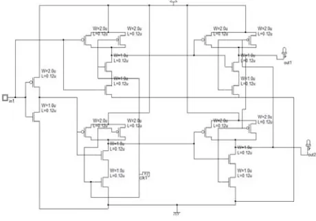
The D Flip Flop can be implemented in different transistor logic such as Static, Dynamic, Pseudo NMOS ,True single phased clock , double edge triggered clock and so on. Different logic comes with different transistor structure and analyzed its performance in terms of area, delay and power. Here an D Filp Flop is constructed and analyzed with 18T, 16T, 15T and 5T structure. The below figures shows D Flip Flop with above mentioned logic structure.
3.1 Problems on existing logic
In the above Flip Flops, the number of elements used for each Flip Flop is increased which will increase the area and hence the power consumption. So in this work it is tried to minimize number of elements used with Pass transistor logic.
3.2 Advantages of Pass transistor logic over other logic
Very efficient in use of transistors and potentially very efficient layout result.
Pass Transistors can usually be minimum size devices.
Static power dissipation is unaffected and
dynamic power dissipation is minimized.
D flip flop can be considered as a basic memory cell because it stores the value on the data line with the advantage of the output being synchronized to a clock.
D flip flops form the basis of shift registers that are used in many electronic device. Many logic synthesis tool use only D flip flop or D latch. FPGA contains edge triggered flip flops. D flip flops are also used in finite state machines.
3.3 Pass Transistor Logic
fully complementary CMOS logic. The Pass transistor symbol is given below, where input B is the periodic clock signal.
The pass transistor is driven by a periodic clock signal represented as B and acts as an access switch to either charge up or charge down the parasitic capacitance Cx, depending on the input signal A. Thus, the two
possible operations when the clock signal is active (B = 1) are the logic "1" transfer (charging up the capacitance Cxto a logic-high level) and the logic "0" transfer
(charging down the capacitance Cx to a logic-low level.
4. Results and comparative tables
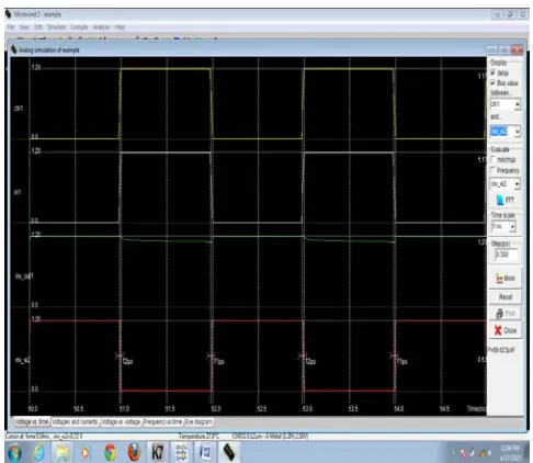
The following figure shows the basic Flip Flop with MOS transistor and with Pass transistor. The Fig.5 shows layout of D Flip Flop with Pass transistor and Fig.6 shows the timing diagram of D Flip Flop with pass transistor.
Fig.4 Logic diagram of D-FF with pass transistor
Fig. 5 Layout diagram of D-FF with pass transistor
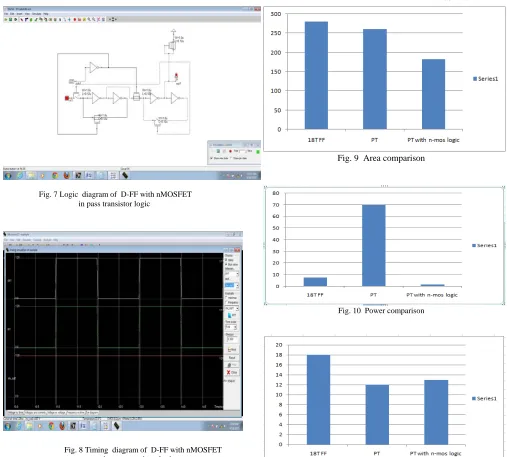
Fig. 7 Logic diagram of D-FF with nMOSFET in pass transistor logic
Fig. 8 Timing diagram of D-FF with nMOSFET in pass transistor logic
Table .1 Comparative table D-FF with different logic structure Type of Flip-flop Area
(µm²)
Power (µw)
Number of Transistors
18T FF 280 7.6 18
Pass transistor logic 261 69.846 12
Fig. 9 Area comparison
Fig. 10 Power comparison
Fig. 11 No. of transistor’s used for different logic
4. Conclusions
References
[1] Noble G, Prof. Sakthivel S.M. “A Novel Flip-Flop Design for Low Power Clocking System”, International conference on Communication and Signal Processing, April 3-5, 2013, India, ©2013 IEEE
[2] N. Nishanth, B.Sathyabhama, “Design of Low Power Sequential Circuit Using Clocked Pair Shared Flip flop”, 2013 IEEE International Conference on Emerging Trends in Computing, Communication and Nanotechnology (ICECCN 2013)
[3] Paneti Mohan & P.C Praveen Kumar, “A Modified D Flip-Flop with Deep Submicron Technology for Electronic Systems”, International Journal of Advanced Electrical and Electronics Engineering, (IJAEEE), 2013.
[4] Shien-Chun Luo, Ching-Ji Huang, and Yuan-Hua Chu, “An Adaptive Pulse-Triggered Flip-Flop for a High-Speed and Voltage-Scalable Standard Cell Library”, IEEE TRANSACTIONS ON CIRCUITS AND SYSTEMS—II: EXPRESS BRIEFS, ©2013
[5] David Li, David Rennie, Pierce Chuang, David Nairn, Manoj Sachdev, “Design and Analysis of Metastable- Hardened and Soft-Error Tolerant High-Performance, Low- Power Flip-Flops”, 12th Int'l Symposium on QualityElectronic Design ©2011 IEEE
[6] Ahmed Sayed and Hussain Al-Asaad, “Low-Power Flip- Flops: Survey, Comparative Evaluation, and a New Design”, IACSIT International Journal of Engineering and Technology, Vol.3, No.3, June 2011
[7] K.G.Sharma, “Modified SET D-Flip Flop Design for Low- Power VLSI Applications”, ©2011 IEEE [8] Jin-Fa Lin, “ Pulse-Triggered Flip-Flop Design with PTL Style Control Scheme”, TENCON ©2011 IEEE
[8] Dinesh sale, Ashwani Rana “Conditional data d flip-flop design using pass transistors for low power application” , 3rd IRF International