Low Power CMOS PLL for Clock Generation
A. Geetha
1, K.Subbulakshmi
2Asst. Professor, Dept. of ECE, Bharath University, Chennai, Tamil Nadu, India1,2
ABSTRACT: In this paper we propose a Low Power Phase Locked Loop (PLL) using transmission gate logic (TG).The proposed PLL has a simpler structure using very less number of transistors compared to the conventional PLL and results in better performance than any other published PLL‟s due to no DC leakage currents and reduced transistor count. The PLL has a dead zone less than 0.01ns in the phase characteristics and has low phase sensitivity errors. The PLL is independent from the duty cycle of input signals and the effects of clock feed – through are reduced by separating the output stage from UP and DOWN signal. The PLL is designed using 0.8 µm CMOS technology .We compared the proposed PLL with the conventional PLL with respect to performance and power consumption. The Results show 30% reduction in power consumption over a conventional PLL with comparable performance.
KEYWORDS: Low Power, PLL, Phase and Frequency Detector, Mixed signal circuits
I. INTRODUCTION
The minimum channel length of the transistor will be scaled down to 0.065 um in 2007, according to the roadmap of semiconductors. In addition to this downscaling, today‟s system-on-chip (SoC) trend forces analog and digital integrated circuits (ICs) to be integrated on a single chip called the complete SoC. At present, there are many demands on the complete SoC in wireless and broadband communications – wireless networking (WLAN, voice/data communication, and Bluetooth), wired communication (WAN and LAN), and consumer electronics (DVD, MP3, digital cameras, video games, and so on). Therefore, as one of the mixed-signal Ics, Phase-Locked Loop (PLL) must follow this complete SoC trend. This chapter introduces the challenges in designing PLL and possible solid-state technologies for the complete SoC trend.
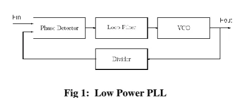
Fig 1: Low Power PLL
The Low Power phase locked loop (PLL) circuit is used to synchronize an output signal, which is usually generated by an oscillator, with a reference or input signal in Frequency as well as in phase. In the synchronized state, the difference (error) between the reference and the oscillator output is zero or at least very small. So it is called „locked‟. The whole circuit consists of three main parts. They are phase & frequency detector (PFD), charge Pump, loop filter (LP) voltage control oscillator (VCO) and divider. The diagram of the PLL is shown in Figure 1.
ISSN (Print) : 2320 – 3765 ISSN (Online): 2278 – 8875
I
nternational
J
ournal of
A
dvanced
R
esearch in
E
lectrical,
E
lectronics and
I
nstrumentation
E
ngineering
(An ISO 3297: 2007 Certified Organization)
Vol. 3, Issue 11, November 2014
10.15662/ijareeie.2014.0311132
In section II, the proposed Novel Low Power Phase Locked Loop is described. The results of proposed PLL circuit are presented, and comparisons are made in section III. In section IV, draws a conclusion.
II. DESIGN OF NOVEL LOW POWER PLL
This section provides detailed information about the proposed PLL, including its major components. Also important characteristics of the PLL are introduced for simulation and analysis, which will be described in this section.
A. Phase and frequency detector
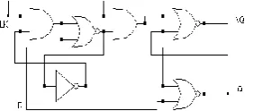
The input phase errors are detected by Phase and Frequency Detector (PFD). These phase or frequency errors are converted into current or voltage to control the output frequency of Voltage Controlled Oscillator (VCO) by charge pump in a charge pump PLL. PFD detects a phase error between the reference signal and the output signal of PLL and the error detection range can be extended with PFD. A conventional CMOS PFD [1] is shown in Fig.2 has large dead zone in phase characteristics at the steady state which generates a large jitter in clocked state in PLL and consumes large amount of power, which cannot be avoided in high frequency operations because internal nodes of PFD are not completely pull up or pull down. The additional prescaler circuits can be added to lower the frequency of the input signals. However, as the division ratio increases, the steady state phase error will increase. The capture range of PLL is determined by the error detection range of PFD. A conventional CMOS PFD has no limit to the error detection range. Therefore, the capture range of PLL is only limited by the Voltage Controlled Oscillator (VCO) output frequency range [5].
Our novel PFD uses a two multiplexers, as the phase difference between the input decreases, the pulse width on UP or DOWN also decreases. These simultaneous up and down signals in the steady state of the PLL create a short circuit in the charge pump which results in a perturbation on LF voltage and produce jitter .To limit the LF voltage perturbation without having a dead zone, we have reduced the minimum UP and DOWN pulse widths by reducing the reset delay in the PFD.Moreover , the linearity of the PFD is affected by this minimum pulse width on UP and DOWN when there is no phase difference between the inputs of the PFD.The new PFD has no dead zone and the nonlinearity near the steady state of the PLLis reduced. This implementation also reduces the transistor count to a large extent.
Fig.2. Conventional PFD Schematic
The conventional phase and frequency detector (PFD) uses a two D-flip-flop (DFF) structure shown fig (1). The DFF has been simplified and implemented using a two 2:1 multiplexer as shown fig (4), is optimized to obtain a minimum PFD delay with reduced power consumption. This new PFD schematic has a reduced delay because the number of serial MOS devices in each gate is limited. The new PFD results in a reduced dead zone and non-linearity near the steady state of the PLL.
Fig 3: DFF Using 19 MOS Transistors
19 MOS transistors shown in fig 3 Based on this DFF, fig 4 shows the PFD according to fig 3 depicted uses 42 MOS transistors, the reset signal R is controlled by NQ .[2-4
In the design of our novel PFD the 2:1 multiplexer replaces the each DFF of fig 3, shown in fig 5 .The PFD using two 2:1 multiplexer uses 9 MOS transistors. The Multiplexers are designed using transmission
Fig. 4. Phase And Frequency Detector
The design of the new PFD has been performed using an asynchronous race free design method. A detailed description of this design methodology[6]
Fig. 5 Novel PFD Using Multiplexer
ISSN (Print) : 2320 – 3765 ISSN (Online): 2278 – 8875
I
nternational
J
ournal of
A
dvanced
R
esearch in
E
lectrical,
E
lectronics and
I
nstrumentation
E
ngineering
(An ISO 3297: 2007 Certified Organization)
Vol. 3, Issue 11, November 2014
10.15662/ijareeie.2014.0311132
The architecture of our novel PFD has one three input NAND gate and two 2:1 multiplexers. One of the input of the NAND gate is always made high and the other input are UP and DOWN signals .The selection input of multiplexer (1) is CLK and of multiplexer (2) is output of VCO.The output of the NAND gate is given to the input i0 of both the multiplexers and the input i1 of the both the multiplexer are grounded. [1]
Table II
Calculated Power At 120 Mhz @1.35V
The operation of the our novel PFD, if CLK is active before VCO the UP output is generated because the CLK given to selection input of the Multiplexer (1) is activated before VCO and the UP value is high so the reset value is low which in turn makes the input to be same .while DOWN is produced if VCO is active before CLK because the VCO given to selection input of the Multiplexer (2) is activated before CLK. As soon as the two clock signals are simultaneously active at the same time, ideally neither UP or DOWN has to be set. In such case, the reset signal R is given to the NAND gate becomes high and therefore the output value changes to low which depicts the reset state of DFF. This results in lower jitter and better linearity near steady state without dead zone and reduced power consumption.[5]
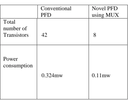
Table I
Calculated Area (With Parasitic Coupling Capacitance Extracted From Layout) The Output Peak To Peak Jitter At120mhz @1.35V
Conventional PFD
Novel PFD using MUX Total
number of Transistors
42
8
Power consumption
0.324mw 0.11mw
Conventional PFD
Novel PFD using MUX Dead Zone
(Jitter) < 10ps < 8ps Layout Area
(mm2)
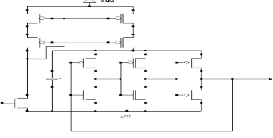
Figure 6: Charge Pump
B. Charge Pump
A charge pump consists of two switched current sources that pump charge into or out of the loop filter according to two logical inputs. [7]The circuit has three states .Charge pump consists of two PMOS and two NMOS, which are connected serially. Both of the NMOS are in the pull down section and both of the PMOS are in the pull up section. The gate of uppermost PMOS is connected to GND The gate of lowermost NMOS is connected to VDD. The gates of the remaining NMOS and PMOS are connected to the "Down" and "Up" pin of the output of PFD. The width of the uppermost PMOS is 15 um and the length of it is 7.5 um. The width of the other PMOS is 30 um and length of it is 600 nm. The width of the lowermost NMOS is 7.5 um and length of it is also 7.5
um
. The width of the other NMOS is 15 um and the length of it is 600 nm.[11]C. Low Pass Filter
The Filter used here is a simple low pass Filter.
It
is comprised of a capacitor and a resistor. The resistor value is 300 k ohm and capacitor is 10 pico farad. The control voltage for the VCO is taken parallel to the capacitor. The values of the component here are taken iteratively. Basically these values allow control voltage to be stable so that small changes or interferences do not affect the locked stage.[13]
D. Voltage Controlled Oscillator
As far as the PSNR and low-supply voltage operation are concerned, the VCO is the most critical block because its internal noise results directly in jitter. Moreover, low-voltage operation limits the design options. To obtain a fully integrated PLL, a current-controlled ring oscillator (CCO) is the basic element of the VCO .It allows low-voltage operation, since no additional capacitances have been used on internal nodes other than the ones created by the
ISSN (Print) : 2320 – 3765 ISSN (Online): 2278 – 8875
I
nternational
J
ournal of
A
dvanced
R
esearch in
E
lectrical,
E
lectronics and
I
nstrumentation
E
ngineering
(An ISO 3297: 2007 Certified Organization)
Vol. 3, Issue 11, November 2014
10.15662/ijareeie.2014.0311132
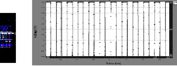
Figure 8: Output of Phase Locked Loop during the locked condition of input and VCO signal.
of white noise in the CCO and given an operating frequency, it can be shown that the voltage across the CCO is minimum and depends only on process parameters which are the best case for a given process. Then as the supply voltage is specified, the maximum saturation voltage of the mirror supplying the current to the CCO is determined. Working down to 1.2V, it is not possible to use a cascoded mirror because the saturation voltage of such a mirror is too high for the expected PSNR. Therefore, to ensure a maximum PSNR even at low-supply voltages, a new circuit called active cascode has been used.[10]
The high-frequency PSNR is mainly determined by the ratio of the parasitic capacitance of the mirror MOS devices and the filtering capacitor across the CCO. [12]This last capacitor cannot be increased too much because it introduces a pole in the PLL that can make it unstable. The size of the mirror devices is determined by the maximum allowable saturation voltage. The stability of this active cascode is ensured by the resistor R between the input and output of the mirror. The relation between current and frequency in this CCO is not linear. To a first approximation, the frequency depends on
the square root of the
current for a voltage across the CCO much larger than the maximum threshold voltage of PMOS or NMOS devices. To obtain a linear gain for the VCO, the voltage to current converter should have a quadratic transfer function. This is achieved by using a MOS device in strong inversion.[14]EDivider
Frequency Divider divides the output frequency before feeding it to PFD. It takes input from VCO and divides the frequency, which is the dclock signal. The Frequency Divider designed for the PFD DPLL is programmable. It takes 8 bit input to divide the frequency so the frequency can be divided by 1 to255 times. The Frequency Divider has three basic parts - an 8-bit synchronous counter, an array of 2input XNOR gates to take input bits and an 8 input Nand gate. The schematic of the Frequency Divider is shown in the Figure 3.6 .The Jitter introduced by these dividers is cancelled by a D Flip flop that resynchronizes the output signal of the dividers with the output frequency of the PLL.The divider is implemented using transmission gate , therefore there is drastic reduction in the transistor count.[15]
III. RESULTS AND DISCUSSION
Verifications for logic, timing simulations are done by using Modelsim, power estimations and final layout without any DRC and LVS problems using Microwind is also shown in Fig.9[16-20]
Figure 9: Layout Of Low Power CMOS Phase Locked Loop
IV. CONCLUSION
circuit shows that it is possible to overcome the issue of PLL short settling time by using a very low power PFD operating even in idle mode. So, the recovery time from idle mode to normal mode is virtually zero. The PFD is designed using 0.8 µm CMOS technology
REFERENCES
[1] V.Von Kaenal ,”A 320 Mhz ,1.5 mw @ 1.35V CMOS PLL for microprocessor clock generation “in ISSCC „‟96
[2] Prabhakar J., Senthilkumar M., Priya M.S., Mahalakshmi K., Sehgal P.K., Sukumaran V.G., "Evaluation of Antimicrobial Efficacy of Herbal Alternatives (Triphala and Green Tea Polyphenols), MTAD, and 5% Sodium Hypochlorite against Enterococcus faecalis Biofilm Formed on Tooth Substrate: An In Vitro Study", Journal of Endodontics, ISSN : 0099-2399, 36(1) (2010) pp. 83-8
[3]James Montanaro “ 160 Mhz 0.5W CMOS Risc Processor “in ISSCC 96
[4]M.Van Pamel “ Analysis of charge pump for PLL‟s” IEEE Trans. July 99
[5] Ramkumar Prabhu, M., Reji, V., Sivabalan, A., "Improved radiation and bandwidth of triangular and star patch antenna", Research Journal of Applied Sciences, Engineering and Technology, ISSN : 2040-7459, 4(12) (2012) pp. 1740-1748.
[6] A. Maxim, “A 0.16-2.55-GHz CMOS active clock deskewing PLL using analog phase interpolation,” IEEE J. Solid-State Circuits, vol. 40, no. 1, Jan. 2005, pp.110 – 131.
[7] Saravanan T., Saritha G., Udayakumar R., "A Robust H-infinity two degree of freedom control for electro magnetic suspension system", Middle - East Journal of Scientific Research, ISSN : 1990-9233, 18(12) (2013) pp. 1827-1831.
[8] J. Kim, J-K. Kim, B-J. Lee, N. Kim, D-K. Jeong, and W. Kim, “A 20-GHz phase locked loop for 40-Gb/s serializing rransmitter in 0.13-µm CMOS,” IEEE J. Solid-State Circuits, vol. 41, no. 4, Apr. 2006.
[9] Saravanan, T., Saritha, G., "Buck converter with a variable number of predictive current distributing method", Indian Journal of Science and Technology, ISSN : 0974-6846, 6(S5) (2013) pp.4583-4588.
[10] C-M Hung and K. O. Kenneth, “A fully integrated 1.5-V 5.5-GHz CMOS phase locked loop,” IEEE J. Solid-State Circuits, vol. 37, no. 4, Apr 2002.
[11] Saravanan, T., Srinivasan, V., Sandiya, V.P., "A two stage DC-DC converter with isolation for renewable energy applications", Indian Journal of Science and Technology, ISSN : 0974-6846, 6(S6) (2013) pp. 4824-4830.
[12] Z. Wang, “An analysis of charge-pump phase-locked loops,” IEEE Trans. on Circuits and Systems I, vol. 52, no. 10, Oct. 2005.
[13] P. K. Hanumolu, M. Brownlee, K. Mayaram, and U-K. Moon, “Analysis of charge pump phase-locked loops,” IEEE Trans. on Circuits and Systems I, vol. 51, no. 9, Sep, 2004.
[14] R. B. Staszewski and P. T. Balsara, “Phase-domain all-digital phase-locked loop,” IEEE IEEE Trans. on Circuits and Systems II, vol. 52, no. 3, Mar. 2005.
[15] B. Razavi, Design of Analog CMOS Integrated Circuits, 2nd Ed., New York: McGraw-Hill, 2001. [16] W. Chen. The VLSI Handbook. CRC Press, Boca Raton, FL, 2000
[17]R.J. Baker, H.W. Li, and D.E Boyce. CMOS Circuit Design, Layout, and Simulation.IEEE Press, New York, NY 1998 [18] R.E. Best. Phase-Locked Loops, 3rd Ed. McGraw Hill 1997
[19]Phillips Semiconductors, “An overview of Phase Locked Loops”, AN177,Application Note,Dec. 1988. [20]Phillip Allen, Douglas Holberg, “CMOS Analog Circuit Design”, Oxford Univ Press., Feb2002
[21] TVUK Kumar, B Karthik, EB Kumaran, Visual Secret Sharing Scheme for JPEG Compressed Images, Middle-East Journal of Scientific Research 12 (12), PP 1873-1880, 2012.
[22] B Karthik, TVUK Kumar, EMI Developed Test Methodologies for Short Duration Noises, Indian Journal of Science and Technology 6 (5S), PP 4615-4619, 2013.
[23] Mr.B.Karthik, Dr.T.V.U. Kiran Kumar, N. Gomathi, Immobilizer Implementation using Mutual Authentication with enhanced security using 802.15.4 protocol,International Journal of Advanced Research in Electrical, Electronics and Instrumentation Engineering ,ISSN 2278 - 8875, pp 142-151, Vol. 1, Issue 3, September 2012.
[24] M.Jasmin,Bus Matrix Synthesis Based On Steiner Graphs For Power Efficient System On Chip Communications ,International Journal of Advanced Research in Electrical, Electronics and Instrumentation Engineering, ISSN 2278 - 8875 , pp 98-104,Vol. 1, Issue 2, August 2012. [25] M. Jasmin, A Low Power Pipelined FFT/IFFT Processor for OFDM Applications,International Journal of Advanced Research in Electrical, Electronics and Instrumentation Engineering,ISSN (Print) : 2320 – 3765, pp 4712-4721, Vol. 2, Issue 10, October 2013.
[26] M Jasmin, Low Power Design of the Processer Based on Architecture Modifications,International Journal of Advanced Research in Electrical, Electronics and Instrumentation Engineering,ISSN: 2278 – 8875, pp 2922-2927, Vol. 2, Issue 7, July 2013.
[27] K.Subbulakshmi,Implementation for SMS4-GCM and High-Speed Architecture Design,International Journal of Advanced Research in Electrical, Electronics and Instrumentation Engineering, ISSN (Print) : 2320 – 3765, pp 10965-10970, Vol. 3, Issue 8, August 2014.