Module. (Under the direction of Dr. Douglas C Hopkins).
This research developed a fabrication process for novel 3D chip-on-chip power modules for the NCSU-PREES laboratory. Past and present 3D power module packaging technologies have been reviewed, and flex-circuit-based chip-on-chip approach has been selected to demonstrate fabrication processes to produce very high power density modules. Based on this concept, the flex circuit and testing circuit topologies have been designed with the assist of electrical and thermal simulations. Because flex materials have low modulus, mechanical stress analysis was not pursued for this particular research. An extra need of the module is double-sided solderable power devices since the devices will be sandwiched between different flex circuit layers in the module to realize electrical and thermal connections. This required a surface metallization process to be developed at the NCSU-NNF facility to convert Al die pads to solderable Ag or Cu. A Ti/Ni/Cu metallization solution has been chosen to deposit on Al pads of the devices. Lastly, the flex circuits and test circuits have been assembled and tested to show fabrication process success.
by Mingyu Yang
A thesis submitted to the Graduate Faculty of North Carolina State University
in partial fulfillment of the requirements for the degree of
Master of Science
Electrical Engineering
Raleigh, North Carolina 2015
APPROVED BY:
_______________________________ ______________________________ Dr. Douglas C Hopkins Dr. Subhashish Bhattacharya Committee Chair
DEDICATION
BIOGRAPHY
Mingyu Yang was born in Harbin, Heilongjiang Province in People’s Republic of China. He received his Bachelor of Science degree in Electrical Engineering from Huazhong University of Science and Technology, Wuhan, China. He is a graduate of North Carolina State
ACKNOWLEDGMENTS
First, I would like to gratefully and sincerely thank my advisor, Dr. Douglas C Hopkins, for his kindly instruction and help in this research. This work could not have been finished without his guidance, support and time.
I would also like to thank Dr. Subhashish Bhattacharya and Dr. Wensong Yu to be my committee member. Their suggestions and help in my study are greatly appreciated.
The colleagues at PREES lab and FREEDM center also give me a lot of help during the entire research. I would like to thank Yang Xu, Haotao Ke, Adam Morgan, Sean Ketring, Liqi Zhang, Xin Zhao, Xiao Zhang, Yang Lei, Junning Jiang, Yifan Jiang, Juncheng Zhou, Xinyu Zhang, Youxi Shao, Qinmiao Li, Shangmin Lin, Hongyu Wu, Dr.Xijun Ni, Anjie Jiang, Qian Wu, Jingwen Xiong, Lisha Sun, Yue Shi for their help, discussions and friendships.
I would also like to acknowledge the laboratory support from Hesse Mechatronics and Sikama companies for donating equipment that made this research work more professional, much easier and quickly possible, and from CREE for bare die and Fairchild.
TABLE OF CONTENTS
LIST OF TABLES………....……….viii
LIST OF FIGURES …..………...ix
CHAPTER 1 INTRODUCTION ... 1
1.1 Background ... 1
1.2 Overview of Stacked Chip Power Module ... 5
1.3 Problem Statement and Objective ... 9
1.4 Methodology ... 11
1.5 Thesis Outline ... 13
CHAPTER 2 TOPOLOGY AND DEVICE CHARACTERISTICS... 14
2.1 Bare Chip Characteristics ... 14
2.2 Circuit Topology and Design ... 18
2.3 Flex Circuit Development ... 20
2.3.1 Layout Challenges ... 20
2.4 Test Circuit Development ... 26
2.5 Simulation Results... 27
2.5.1 Electrical simulation ... 27
2.5.2 Thermal simulation ... 34
CHAPTER 3 MODULE MATERIALS AND FABRICATION PROCESS ... 41
3.1 MOSFET and Diode... 41
3.1.1 Metallization Preparation ... 41
3.1.2 Metallization process ... 42
3.1.3 Pull test and results ... 49
3.2 Flex circuit... 50
CHAPTER 4 ASSEMBLY, TESTING AND RESULTS ... 51
4.1 Power Module Assembly ... 51
4.2 Electrical Characterization ... 60
CHAPTER 5 SUMMARY AND FUTURE WORKS... 63
REFERENCES ... 65
APPENDICES ... 68
LIST OF TABLES
Table 2-1 Power device electrical specifications ... 15
Table 2-2 FAN3122C specifications ... 17
Table 2-3 Circuit specifications ... 18
Table 2-4 Passive components ... 19
Table 2-5 Thermal characteristics ... 37
Table 3-1 Deposition process and thickness obtained ... 47
LIST OF FIGURES
Figure 1-1 Typical power multi-chip module ... 2
Figure 1-2 Double-sided flexible PCB ... 4
Figure 1-3 IPEM using flex circuit ... 6
Figure 1-4 Flex-circuit based power module ... 7
Figure 1-5 Comparison of standard connection technology (solder/bonding) and SKiN technology ... 8
Figure 1-6 TI PowerStack technology ... 9
Figure 1-7 Cross sectional view of flex module ... 10
Figure 1-8 Fabrication flow chart ... 12
Figure 2-1 Power devices dimension ... 15
Figure 2-2 FAN3122C die attachment diagram ... 17
Figure 2-3 Reverse buck converter ... 18
Figure 2-4 Double layer double access part ... 21
Figure 2-5 Single layer double access part ... 21
Figure 2-6 Incorrect gate driver footprint for wire bonding and not flip-chip ... 22
Figure 2-7 Gerber files and fabricated circuits ... 23
Figure 2-8 PCB design file in Altium Designer... 26
Figure 2-9 PCB circuit ... 27
Figure 2-10 Critical loop in buck power stage... 28
Figure 2-11 Gate drive turn-on and turn-off current path ... 29
Figure 2-12 Reverse buck topology ... 31
Figure 2-13 Output voltage waveform ... 32
Figure 2-14 Steady state inductor current ... 33
Figure 2-15 Module top view ... 39
Figure 2-16 Module bottom view ... 40
Figure 3-1 Single-layer double-access flex ... 50
Figure 3-2 E-beam evaporator ... 43
Figure 3-3 Ti deposition sample ... 44
Figure 3-4 Raw data obtained from Nanometrics ... 45
Figure 3-5 Mechanical chips on metal plate ... 46
Figure 3-6 Samples after process ... 48
Figure 3-7 MOSFET samples under microscope... 48
Figure 3-8 Pull test set up ... 49
Figure 4-1 Size comparison of flex circuit parts and one cent coin ... 52
Figure 4-2 Sikama conduction belt reflow oven ... 53
Figure 4-3 Reflow temperature profile ... 54
Figure 4-4 Semi-finished module after Step 1 ... 54
Figure 4-5 Solder paste on pads ... 55
Figure 4-6 Part A with components ... 56
Figure 4-8 Semi-finished module after Step 2 ... 56
Figure 4-9 Bottom sides of Part A and B ... 57
Figure 4-10 Part B assembly status ... 57
Figure 4-11 Solder paste on pads ... 58
Figure 4-12 Flex module before reflow process ... 59
Figure 4-13 Finished flex module ... 59
Figure 4-14 Finished system assembly ... 60
Figure 4-15 Test bench set up ... 61
CHAPTER 1 INTRODUCTION
This chapter gives a basic background of power electronic module design. A section of literature review is included to show state-of-the-art packaging technologies. The motivation and methodology of this research will also be addressed.
1.1 Background
Power electronic modules are widely used in power electronic systems, such as switching power supplies, motor drives and electric vehicles. The packaging of power electronics is a critical factor to performance and reliability of power electronics systems [1]. The current R&D focus on power electronic packaging is on cost reduction, increase of power density, increase of reliability and reduction of effects due to parasitic elements. These parasitics are undesirable capacitance between circuit parts and inductance in circuit traces. They both can have a negative effect, such as increases in electromagnetic radiation and switching loss. Therefore, designers and manufacturers try to minimize the parasitic elements of the
Figure 1-1 Typical power multi-chip module [3]
devices increase, the di/dt is getting faster [4]. Therefore, the stray inductance inside the module plays an ever more important role in high current and high frequency operation.
The objective of this work is to develop a packaging fabrication method suitable for chip-stack technology and apply flexible PCB circuit technology for interconnection to reduce the stray inductance to realize high power density. The 3D chip-stack advantages are:
Smaller Footprint: more functionality fits into a smaller space
Shorter interconnect: the average interconnect length is reduced and thus stray inductance
is reduced as a result
Higher power: flexible circuit connection leads to higher power capability by choosing
heavy Cu layer up to 5 ounce (175µm/6.9mil) thick
Flexible printed circuit, also known as flex circuit or flexible PCB, is a technology for
assembling electronic circuits by mounting electronic devices on flexible polymer substrates, such as polyimide [5]. Flexible circuits can be manufactured using identical components of small size as used in rigid printed circuit boards, but allowing the circuit to flex during use. This is the major reason why fabrication of flex circuitry was chosen for the thesis work. Flex circuits also have other benefits compared to traditional rigid boards, e.g.
Higher circuit density
More robust operating temperature range
Improved reliability and impedance control
Size and weight reduction
Elimination of mechanical connectors, such as lead frame in traditional modules
The objective of this thesis is to develop and demonstrate in the NCSU-PREES laboratory the fabrication processes to create stacked power electronic circuits, which can realize the above advantages.
There are a few approaches to flex circuit construction. The most common from simple to complex may include single-layer single-access flex circuits, single-layer double-access flex, double-sided flex, multilayer flex and rigid-flex circuits. Double-sided flex will be used in the thesis, and the design and fabrication details will be covered in Chapter 2. As an example, Figure 1-2 shows the cross sectional view of a double-sided flexible circuit.
1.2 Overview of Stacked Chip Power Module
Flip-Chip technology was firstly introduced in the IC industry as a low cost, high density and reliable chip attachment approach. [7] Bonding wires are eliminated in this method. Instead, solder joints are utilized for interconnection and provide more current capability with lower parasitic inductance and capacitance. In addition, the flip-chip package also becomes smaller since it does not need a lead frame. This section, we will go through some of the existing research and state-of-the-art technologies of flip-chip and flex circuit technology.
In the paper ‘Power Electronics Modules for Inverter Applications using Flip-Chip on
Flex-Circuit Technology’, researchers from Rensselaer Polytechnic Institute and University of
Figure 1-3 IPEM using flex circuit [8]
In the paper ‘Flip-Chip on Flex Integrated Power Electronics Modules for High-Density Power Integration’, researchers from Virginia Tech presented a high-density power module
Figure 1-4 Flex-circuit based power module [9]
On the industrial side, Semikron has developed a technology which they named SKiN Technology, using multiple flex layers made up of flex foil. Figure 1-5 shows the difference between standard power module package and SKiN Technology. As can be seen, the
traditional wire bonding is substituted by flex layers, and also all soldering and bond connections are replaced by sintered compositions. According to Semikron’s experimental
data, advantages lie in the aspects below:
Thermal resistance between semiconductor and coolant is decreased by 30%
Bond wires can only make contact to about 21% of the total metallized chip surface,
while sintered flex foil exhibits a die contact area of up to 85%. This leads to a 60% reduction of inner commutation inductance.
Without wire bonding and lead frame, power density is increased by 50% in this 3D
a) Standard Technology b) SKiN Technology
Figure 1-5 Comparison of standard connection technology (solder/bonding) and SKiN technology [10]
Texas Instrument’s PowerStack technology also provides another solution for 3D
a)b)
Figure 1-6 TI’s PowerStack technology [11]
1.3 Problem Statement and Objective
This research develops a procedure in the NCSU Laboratory for Packaging Research in Electronic Energy Systems (PREES) for fabricating stacked components, such as a MOSFET, diode and gate driver, to create a single module. A demonstration module is constructed with flex-circuit technology with focus on process development and
double-sided flex circuit, i.e. the MOSFET and diode are both soldered to same piece of flex circuit. Extensions to this flex circuit also plays the role of interconnect to realize the
connection between power module and outer PCB circuitry. Similarly, the MOSFET source (top-side) is soldered to another flex circuit which hosts the gate drive control circuitry. Hence, the MOSFET and diode are sandwiched by two pieces of flex circuit as shown Figure 1-7. Finally, the module is tested in a buck topology. Electrical connection is covered in Chapter 2.
In order to solder bare die, i.e. MOSFET and diode, onto flex circuit, additional surface metallization processes are necessary for the devices. After the semiconductor device
becomes solderable, the device is soldered by a reflow process. During the reflow processes, different melting temperature solders should be applied to the joints between devices and circuits so that multiple reflows become feasible.
1.4 Methodology
From electrical design point of view, power modules are normally quite simple to be designed [12]. However, a lot of issues are associated with thermal management, material selection and reliability of the 3D structure because the power modules are always pursuing higher voltage, current, frequency as well as higher level integration capabilities. This thesis work is comprised of four major steps which are literature review and idea proposal,
establishing design guidelines for chip-stack power module, electrical and thermal simulation, and power module physical testing.
Literature reviews have been done for several packaging technologies, such as flip-chip, 3D (stacked chip) packaging, direct work in stacked power chips, and reports on publications relevant to designing a chip-stack power module.
The designed chip-stack power module aims at 1600W with 400V input voltage and 4A input current. Thermal management is a crucial part of the design. Therefore, electrical and thermal simulation plays an important role in designing the system topology.
in a typical buck converter circuit. Electrical characteristics, such as gate signal, conductive current, drain to source voltage and turn-on and turn-off transient waveforms can be
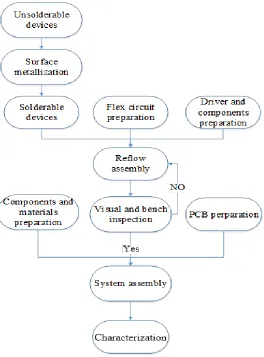
monitored. For the construction of this 3D power module, a fabrication flow chart is shown in Figure 1-8.
1.5 Thesis Outline
This thesis consists of the following chapters:
Chapter 1 introduces the stacked chip power module, states thesis topic and problem and reviews relevant literatures.
Chapter 2 proposes a chip-on-chip MOSFET power module topology for a stacked MOSFET, diode and gate driver chips. This chapter also introduces the characteristics of the bare die MOSFET, diode and Fairchild’s gate drive chip. Simulation results are provided to show module’s performance.
Chapter 3 introduces the material and gives detailed procedures for fabricating a module. Process procedures and results are also given for providing a solderable interface in place of aluminium pads on the chips.
Chapter 4 provides the test board assembly and test results.
CHAPTER 2 TOPOLOGY AND DEVICE CHARACTERISTICS
This chapter introduces the characteristics of the power devices and the gate drive chip. Electrical circuit design is shown as two parts, flex circuit module and PCB test circuit motherboard. Electrical and thermal simulation is developed in Simplis®SIMetrix and Comsol to assist the system design.
2.1 Bare Chip Characteristics
a) MOSFET chip dimensions b)Diode chip dimensions Figure 2-1 Power devices dimension [13] [14]
Table 2-1 Power device electrical specifications [13] [14] Component Specifications
MOSFET: CPM2-1200-0025B
Drain source breakdown voltage: 1200V Continuous drain current: 50A@120⁰C
Gate threshold voltage: 2.3V Gate-source voltage: -10/+25V gfs: 22S
Table 2-1 (continued) Coss:220pF Diode:
CPW5-1200-Z050B
Breakdown voltage: 1200V Maximum DC current: 50A
DC forward voltage: 1.6V@50A,25⁰C
Figure 2-2 FAN3122C die attachment diagram [15]
Table 2-2 FAN3122C specifications [16]
Parameter Value
Supply voltage range VDD 4.5-18V Input logic high threshold 55%xVDD
Peak sinking current 11.4A
2.2 Circuit Topology and Design
The power module is designed for placement into a buck converter topology. Figure 2-3 shows a traditional buck schematic with the power MOSFET and inductor on the low side. Gate driver shares the same ground as the power circuit which makes control easier.
Figure 2-3 Reverse buck converter
The passive components are designed and selected based on buck converter design requirements, as shown in Table 2-3.
Table 2-3 Circuit specifications
Vin 400V
Vout 160V
Iout 10A
Fsw 500kHz
Table 2-3 (continued)
ΔVout(peak to peak) 1%
Pout 1600W
The following ideal passive component values are selected based on the specifications above.
Table 2-4 Passive components
Component Value
Output capacitor 1uF
Inductor 64uH
Resistive load 16ohm
In addition, 1uF ceramic capacitors should be applied to both input and output as bypass capacitors since the design aims at 500kHz switching frequency which is a relatively high operating frequency. These ceramic capacitors also reduce the equivalent series resistance and inductance (ESR and ESL) of the bulk capacitor and output capacitor since ceramic capacitors have extremely low parasitic elements. These will improves the efficiency and switching performance.
2.3 Flex Circuit Development
There are three flex parts needed for the flex power module. First is used as interconnection between gate driver and MOSFET, which has a double layer double access feature. Gate drive bare die is flipped and attached to the top side of this layer as well as a 0.1uf bypass capacitor and gate resistor in a 0805 standard package. The power MOSFET die is attached to the bottom side of the layer. Gate signal generated by a signal generator is amplified by gate driver and applied to the MOSFET gate through vias. Copper traces are extended and solderable pads are placed at both ends of the part in order to make electrical connection with the PCB mother board. Figure 2-4 is the actual circuit picture.
2.3.1 Layout Challenges
circled in red is where a mistake occurred due to misinterpretation in the layout files. The pads should be solder filled. Unfortunately, the Cu trace was covered by insulated material. After communication with the manufacturer, we found a misunderstanding happened because the part was designed with “partial” double-layer double-access and “partial” single-layer double-access, which are not standard for manufacturing. The other two parts which are single-layer double-access parts have similar issues as shown in Figure 2-5. Designers should be careful when placing single layer and double layer parts on the same panel for fabrication.
Figure 2-4 Double layer double access part
Figure 2-5 Single layer double access part
views. However, since the die flips and is soldered onto the circuit, the landing pattern should be mirrored against the diagram. This is also a critical point that new designers should pay close attention to when creating flip-chip versus wire-bond footprints. Since flex circuits generally require longer turnaround time and higher expense (usually a few hundred dollars for a single-layer panel), a lot of details should be taken into consideration before ordering.
Figure 2-6 Incorrect gate driver footprint for wire bonding and not flip-chip
The final flex circuits were ordered from American Circuits, Inc. of Charlotte, NC. The three parts are modified to be double-layer double-access. By use of vias to create “single-layer double-access” parts, gerber-file layouts and actual circuits for Part A-C are shown side-by-side in Figure 2-7. The Part A is 825x220mil (21x5.5mm); Part B is 625x 410mil
a) Part A top side (Gerber and circuit)
b) Part A bottom side
c) Part B top side
e) Part C top side
2.4 Test Circuit Development
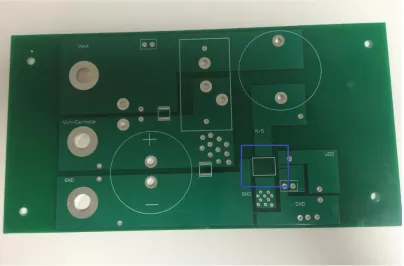
Test circuit development is the circuit design of a FR4 PCB mother board. Altium designer is the circuit design software used in the thesis. The circuit design problems, though not very complicated to a seasoned designed, shows the difficulties in designing flex for a beginner. Figure 2-8 is the PCB circuit under Altium Designer environment. Six solderable pads are available in the blue-square area. However, as it shows in Figure 2-9, pads are covered by epoxy insulation material in the blue-square area. This is because mask relief was absent for these pads. In Altium Design, the Top Solder layer is the solder mask layer. One should always pay attention to make the mask relief for the pads. This issue was resolved in the later chapter by physically removing the insulation and exposing Cu trace.
Figure 2-9 PCB circuit
2.5 Simulation Results
2.5.1 Electrical simulation
Both electrical and thermal simulations are presented in this section. Electrical simulation is based on LTspice® Linear Technology. Circuit functionality and device switching
performance will be checked. In addition, simulation results are also helpful with component selection and thermal analysis.
buck topology, are critical for the overall switching speed. There are two critical loops in the design. One is the AC current loop in the power stage as shown in Figure 2-10. Parasitic inductance between diode and MOSFET can be neglected since they are stacked vertically without any wire or via through the interconnection. The parasitic inductance in the loop is mostly induced by vias between input bypass capacitor and anode of the diode. The PCB via inductance value can be calculated using formula below:
Inductance: L=5.08h×[ln(4h/D)+1] [18]
Where D is the diameter of the via, h is the thickness of the PCB, and H is the length of the via. There are two kinds of vias in the critical loop on the PCB which have the diameter of 94mil and 56mil. For a 1.6mm standard thickness FR4 PCB, one 94mil via will add
L=5.08×0.063× [ln(4×0.063/0.094)+1]=0.64nH. The other 56mil via will add L=0.8nH. On the PCB, there are eleven 47mil vias parallel and ten 28mil vias parallel in the loop. Hence the parasitic inductance of these vias is 0.63nH/11+0.8nH/10=0.14nH
For gate drive control, the current paths for the MOSFET turn-on and turn-off are shown in Figure 2-11. Blue and yellow arrow lines represent the turn-on loops, whereas yellow and red lines represent the turn-off loop. These critical loops play crucial roles on determining the switching speed, and designers should make every effort to shorten the loops and minimize inductance and resistance in the paths.
Figure 2-11 Gate drive turn-on and turn off current paths [16]
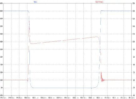
The buck topology constructed in LTspice®Linear Technology is shown in Figure 2-12. Parasitic inductance is included. Notice that the MOSFET and diode model number are different from what we mentioned in previous chapter. In fact, the MOSFET represents the same device, and however diode represents another similar CREE’s device which has 1200V
Figure 2-15 Vdiode & Idiode
2.5.2 Thermal simulation
Thermal analysis calculates the temperature and heat transfer within and between components in the design and its environment. The simulation analysis is conducted in COMSOL Multiphysics® Modeling Software. The flex module is modeled in the software and steady-state heat transfer condition is obtained.
To determine whether or not power devices are suitable for a particular application from a thermal standpoint, it is necessary to calculate their power dissipation. The power devices in the thesis, SiC MOSFET and diode, are major heat sources in the flex module. Heat
devices. The MOSFET power dissipation is mainly made up of two parts, resistive losses and switching losses. The switching MOSFET's resistive losses are calculated using its duty factor and Rds(on):
Presistive = [Ion² × Rds(on)] × (Vout/Vin)
According to the datasheet, Rds(on)=43mΩ @50A, 150˚C which can be used as worst case
condition. In addition, duty cycle and Ion is set to be 40% and 10A respectively. Resistive loss is then obtained as 1.72W.
Calculating the switching MOSFET's switching loss is difficult because it depends on many difficult-to-quantify and typically unspecified factors that influence both on and turn-off. As switching losses per cycle are obtained in the electrical simulation, the following formula is used as a rough approximation to be the first step in evaluating a MOSFET:
Pswitching=fsw×Switching loss per cycle
Where fsw is the targeted switching frequency 500kHz. Switching loss per cycle is 130µJ. Hence, power dissipation of switching losses is 65W. Switching losses should be calculated again once switching waveform is obtained on the lab bench.
Where Vf is DC forward voltage, If is forward current. According to the datasheet,
Vf=1.5V@ 25A, 125˚C. Assume If=10A. Conduction loss is then obtained as 9W. Switching
loss of the diode is calculated based on electrical simulation:
Pswitching=fsw×Switching loss per cycle
Where fsw is 500kHz and switching loss per cycle is 14µJ. Hence, the power dissipation of switching loss is 7W.
Then the flex module is built and studied in COMSOL environment. Figure 2-16 shows how the module is built. The parts in the module are built as blocks. Table 2-5 shows the part dimensions from top to the bottom in the model.
Table 2-5 Part Dimensions
Thickness(mm) Planar dimension(mm)
Part A Cu trace 0.1 5.5×12.3
Solder 2 0.1 3.05×4.54
MOSFET 0.18 4.04×6.44
Solder 1 0.1 4.04×6.44
Part B Cu trace 0.1 16×10
Table 2-5 (continued)
Diode 0.38 5×5
Solder 0.1 5×5
Part C Cu trace 0.1 16×10
MX-4 0.2 6×6
The materials should be assigned to each block after the 3D model is constructed. Table 2-6 shows the thermal characteristics of the materials used in the analysis. Copper is assigned to the flex circuit trace. Silicon carbide is assigned to the power devices. The MX-4 is a non-conductive thermal paste that is used to thermally connect Part C to heat sink. The Sn63Pb37 is a solder that will be described in a later chapter.
Table 2-5 Thermal characteristics
Materials Density (kg/m³) Thermal conductivity (W/(m*K))
Copper 8700 400
Silicon Carbide 3200 450
MX-4 2500 8.5
Figure 2-16 and Figure 2-17 show the steady-state temperature model of the flex module. Figure 2-15 is top view and Figure 2-16 is bottom view. The bottom of the module, which is the thermal paste layer, is set to be room temperature as it is directly connected to bulk heat sink. The extended ends of three flex part are also set to be room temperature since they are connected with the PCB traces directly. The hottest point is located in the MOSFET layer
and reaches 99˚C, which is below the maximum operating temperature of 150˚C in the
datasheet. The thermal paste layer is one of the main reasons that causes this high
CHAPTER 3 MODULE MATERIALS AND FABRICATION PROCESS
This chapter introduces the materials in the module and fabrication process in the lab. The SiC MOSFET and diode are from CREE, Inc and the flex circuit is chosen as the substrate. Surface metallization of the power devices is a major issue addressed in this chapter. However, the base process has been developed, but needs further improvement due to an undesirable metallization result.
3.1 MOSFET and Diode
Currently, most of the devices in commercial power modules are interconnected by bonding wires. Almost all power devices are designed for wire bonding instead of direct solder interconnect. The power MOSFET and diode used in this thesis were acquired from CREE, Inc. For the SiC power MOSFET, it has source and gate pads with approximately 4um thick Al. The backside of the die is the drain, which has a Ag solderable metallization (0.8/0.6um thick Ni/Ag). For the SiC Schottky diode, similarly, it has 4um Al anode metallization and a Ag (1.8um Ni/Ag) cathode metallization, according to the datasheet. Except for the bond pads, the rest of the die is covered with a polyimide passivation to form the insulation between pads and die edges. The absence of solderable metallization on the source and gate pads of the MOSFET, and anodes in the Schottky diodes, has to be addressed to achieve solder interconnection between die and the flexible printed circuit.
Electron beam physical vapor deposition approach (EBPVD) is selected for the metallization process to make the Al pads solderable. For the thin film materials, Ti/Ni/Cu under bump metallization was selected. Target thickness is 200nm/1000nm/200nm respectively. The Ti layer adheres well to the Al surface on the device pads. The Cu layer on top helps with solder wetting as well as acting as an oxidization layer. The Ni layer has three functions: [9]
It acts as a diffusion barrier between Al and Cu, otherwise intermetallic formation
between them could lead to the depletion of the Cu layer, thereby preventing solder wetting.
It is an excellent solder diffusion barrier
It may also provide a solder wetting surface in case Cu on top of the metallization
layers is consumed
3.1.2 Metallization process
Figure 3-1 E-beam evaporator
According to the data, the average thickness of the Ti glass slide is 2194Å. The mean deposition rate then can be calculated by dividing thickness by deposition time.
Figure 3-3 Raw data obtained from Nanometrics
After deposition of each layer of metal, the deposition rate was obtained for each of the three kinds of metal. The rates are 2Å/sec for Ti, 4.5Å/sec for Ni and 0.3Å/sec for Cu. Then three layers of metal were deposited at one time which means to load all metal materials into e-beam chamber and run the entire process without breaking vacuum. The reason of doing this is because metal layers should not be exposed to air during the deposition since the metal may oxidize and prevent the metal vapor from solidifying and sticking to the previous metal layer. Figure 3-4 are mechanical chips (dummy chips) that were stabilized onto metal plate using Kapton tape but left openings at source and gate on MOSFET, and anode on diode.
Scan Parameters
Scan Type Standard Scan
ID 0
Stylus Radius: 12.5 µm
Location -16894.7 um 23841.3 um
Length 1674.0 um
Duration 10 sec
Resolution 0.558 um/sample
Force 10.00 mg
Measurement Range 6.5 um Profile Hills&Valleys Display Range Auto
R. Cursor Pos: 618.8 um Width: 71.8 um M. Cursor Pos: 429.7 um Width: 62.1 um
Analytical Results
Function R.Cur Pos R.Cur Width M.Cur Pos M.Cur Width Result
Figure 3-4 Mechanical chips on metal plate
During the deposition, another issue made the process much slower than estimated. The tool has its own cooling system using water. As the process went on, the water temperature was also rising. According to the equipment manual, temperature of the cooling system should not go beyond 40⁰C, otherwise users should turn off the power until the temperature falls back to laboratory room temperature 17⁰C. Because of this, the deposition of Ni and Cu
Table 3-1 Deposition process and thickness obtained
Metal Heating cycles Deposition time (one cycle) Cooling time (one cycle) Total time Total thickness obtained(A) Average deposition rate(A/sec)
Ti 1 15 10 25 2015 1.34
Ni 5 30 10 200 9295 0.77
Cu 11 30 10 440 1834 0.07
*Time is in minute
Figure 3-5 Samples after process
3.1.3 Pull test and results
Pull test is illustrated in Figure 3-7. Metallized MOSFET die was attached to a direct bonded copper (DBC) plate. A specifically sized pull stud with a rounded end used for this type of testing was soldered onto the metallized side of the MOSFET. The other end was bent for pull test. A force meter was then hooked up to measure the tension. As a result, the peak tension recorded in the pull test is 182g at 2.3x4.0 mm² area which equals to 0.02kg/mm². According to [20], average strength of PVD Cu metallization is larger than 55MPa which equals to 5.5kg/mm². In contrast, the strength of the metallized layers on MOSFET is not enough for the application. As a result, the metallization approach needs to be improved. The improvement should be made will be mentioned in future work in the last chapter.
3.2 Flex circuit
Flex circuits are ordered from American Circuit, Inc. Materials of Part A are depicted in Figure 1-2 where each polyimide layer is 1mil (25.4μm) thick and each Cu layer is 1oz (35μm). The Parts B and C are single-layer double-access, which use the same thickness
materials as Part A. The reason of using single-layer for Parts B and C is because single-layer flex can provide better heat transfer capability than double layer. As it is shown in Figure 1-2, double-layer flex circuits always have an internal insulation material as well as adhesive layers in between the Cu layers which significantly increase the thermal resistance in the path. In contrast, single-layer double access flex is able to create a low thermal resistance path as shown in Figure 3-8. MOSFET and diode are vertically placed on both sides of Part B, since SiC has fairly good thermal conductivity. The thermal path made up of SiC and Cu materials is good for heat dissipation.
CHAPTER 4 ASSEMBLY, TESTING AND RESULTS
This chapter introduces the assembly and testing procedures of the chip-on-chip power module. However, due to failure of chip surface metallization, the actual MOSFET and diode were not used in the process. Since the thesis focuses on developing a fabrication process for the chip-on-chip power module, an identically sized Cu plate was used as substitution for the power devices. As a result, electrical characterization was developed with a wire-bonded power module. These procedures can be repeated once metallized power devices are obtained.
4.1 Power Module Assembly
Figure 4-1 shows the final flex circuit parts. The Part A has four component footprints on it, i.e. gate drive chip, MOSFET, gate drive bypass capacitor and gate resistor. Gate drive chip and MOSFET have the finest footprints that needs much effort to make sure they are
connected well both mechanically and electrically. Since they are on opposite sides of Part A. Two kinds of solder (Table 4-1) with different melting temperatures are needed. The lower temperature solder (Sn63Pb37) is used for all the top side component attachment. The higher temperature solder (Sn10Pb88Ag2) is used for all the bottom side component attachement.
Table 4-1 Two types of solder with different melting temperature
Table 4-1 (continued)
1 Sn63Pb37 183⁰C
2 Sn10Pb88Ag2 268-290⁰C
Figure 4-1 Size comparison of flex circuit parts and one cent coin
The assembly and electrical test process is developed step by step as below: Step1. MOSFET source and gate attachment on Part A
and belt speed was set as 6 inch/min. In addition, because of physical proximity of gate and source pads, short circuit may happen between gate and source and therefore need extra attention. A multimeter can be used to check the insulation between gate and source by probing plated vias. Figure 4-4 illustrates the module status after Step 1 in constrast with the finished module in Figure 1-7.
Figure 4-3 Reflow temperature profile
Figure 4-4 Semi-finished module after Step 1
Step2. Gate driver, capacitor and resistor attachment on Part A
Figure 4-5 Solder paste on pads
Figure 4-7 Part A with components
Figure 4-8 Semi-finished module after Step 2
A similar process is done to Part B in this step. Diode anode should be soldered to the bottom side of Part B using 300⁰C Solder 2 as shown in Figure 4-9 with cathode . Likewise, Part B is
probed at anode and cathode by a multimeter to check electrical conductivity. Figure 4-10 illustrates Part B assemly status. Thus far, pre-assembly of Parts A, B and C is finished.
Figure 4-9 Bottom sides of Part A and B
Step4. Module final assembly
In this step, the top side of Part B should be attached to the MOSFET drain, and the top side of Part C should be attached to diode cathode. Solder 1 was applied on top sides of Part B and C (Figure 4-11), and then three parts were stacked together and placed into the reflow oven (Figure 4-12). Kapton tape is used to stabilize each part since the flowability of liquid solder paste during reflow may cause the parts to drift away from original place. Typically, a solder dam material is applied to confine solder spreading, but is skipped for this
demonstration. The finished flex module is illustrated in Figure 4-13.
Figure 4-12 Flex module before reflow process
Step5. Test circuit assembly
One more reflow process is needed in this step in order to solder the flex module onto the PCB mother board. Other loose componenets can be mounted manually. Figure 4-14 shows the finished system assembly.
Figure 4-14 Finished system assembly
4.2 Electrical Characterization
Electrical characterization is conducted with a traditional wire-bonded power module due to unavailabile solderable power devices. Figure 4-15 shows the testbench set up. Tektronix
AFG 3252 Dual Channel Arbitrary/Function Generator and DPO 2024B Digital Phosphor Oscilloscope were used to perform the test.
Figure 4-15 Test bench set up
safe set-up for the PCB board and module. It was decided to spend more time on pad metalization, since the thesis is to develop the design process.
Gate-source and drain-source voltages are probed and recorded as shown in Figure 4-16. This provides suitable verification that the testing approach could be follwed in flex module design.
CHAPTER 5 SUMMARY AND FUTURE WORKS
This research developed a fabrication process for novel 3D chip-on-chip power modules for the NCSU-PREES laboratory. First, the thesis introduces the background of power
semiconductor modules, and reviews the past and current technologies of power packaging. Based on the past and current packaging technologies, the thesis proposes an idea of 3D chip-on-chip module using flex circuit substrate. The module have three potential advantages against other packaging approaches:
Smaller footprint
Shorter interconnect Higher power capacity
For future works, three other areas should be addressed when designing a chip-on-chip power module.
Parasitic extraction: Ansoft®Q3D extractor would be a good choice to extract the
parasitics of the circuit design. The parasitics can be quantified more accurately by software simulation than by theoretical calculation.
PCB mother board layout: the PCB test board, though not the major work of the
Other improvable issues include separating and shortening ground return of both power and signal loops, the approach to measure Id and so on. These are very specific engineering efforts that require careful and patient considerations.
Zincate treatment: Zincate treatment for aluminum pads on power devices should be
REFERENCES
[1] Wang, Wei. "Power Module with Series-connected MOSFETs in Flip-chip
Configuration." PhD diss., Virginia Polytechnic Institute and State University, 2010. [2] Sheng, William W., and Ronald P. Colino. Power electronic modules: design and
manufacture. CRC press, 2004.
[3] John H.Day. "Power Electronics Challenges for Hybrids", Auto Electronics, 2008.
[4] Li, Shengnan. "Packaging Design of IGBT Power Module Using Novel Switching Cells." PhD diss., University of Tennessee, 2011.
[5] Flexible electronics, Wikipedia, http://en.wikipedia.org/wiki/Flexible_electronics
[6] Fjelstad, Joseph. An Engineer's Guide to Flexible Circuit Technology: Materials, Design, Applications, Manufacturing. Electrochemical Publications, 1997.
[7] Lau, John H. Flip chip technologies. Vol. 1. New York: McGraw-Hill, 1996.
[8] Shah, H. N., Y. Xiao, T. P. Chow, R. J. Gutmann, E. R. Olson, S-H. Park, W-K. Lee, J. J. Connors, T. M. Jahns, and R. D. Lorenz. "Power electronics modules for inverter
applications using flip-chip on flex-circuit technology." 39th IAS Annual Meeting Conference Record, vol. 3, pp. 1526-1533. IEEE, 2004.
[9] Bai, John G., Guo-Quan Lu, and Xingsheng Liu. "Flip-chip on flex integrated power electronics modules for high-density power integration." IEEE Transactions on Advanced Packaging, vol. 26, no. 1, pp54-59, 2003.
[11] Matt Romig, Ozzie Lopez. "3D packaging advancements drive performance, power and density in power devices." Texas Instruments, www.ti.com, Jul.2011.
[12] Haque, Shatil. "Processing and characterization of device solder interconnection and module attachment for power electronics modules." PhD diss., Virginia Polytechnic Institute and State University, 1999.
[13] Cree, Inc. "Silicon Carbide Power MOSFET Z-FET MOSFET." CPM2-1200-0025B datasheet, 2013.
[14] Cree, Inc. "Silicon Carbide Schottky Diode Chip." CPW5-1200-Z050B datasheet, 2013. [15] Fairchild Semiconductor international, Inc. "FAN3122C Die Attachment Diagram." [16] Fairchild Semiconductor international, Inc. "Single 9-A High-Speed, Low-Side Gate Driver." FAN3121/FAN3122 datasheet, 2013.
[17] Jason Arrigo. "Input and Outpu Capacitor Selection." Texas Instruments, Application Report SLTA055, Feb.2006.
[18] Quick-teck. "Tips for PCB Vias Design.", Internal Technical Note EN-00417. [19] Cree, Inc. "Cree C2M SiC MOSFET PSPICE MODEL.", Quick start guide, rev 1.8. [20] Braeckelmann, G., D. Manger, S. C. Seo, S. Beasor, S. Nijsten, and A. E. Kaloyeros. "Deposition of barrier layer and CVD copper under no exposed wafer conditions: adhesion performance and process integration." In Materials for Advanced Metallization, 1997. MAM'97 Abstracts Booklet., European Workshop, pp. 27-29. IEEE, 1997.
[22] Jiang, Li. "Thermo-mechanical reliability of sintered-silver joint versus lead-free solder for attaching large-area devices." PhD diss., Virginia Polytechnic Institute and State
![Figure 1-1 Typical power multi-chip module [3]](https://thumb-us.123doks.com/thumbv2/123dok_us/1655768.1207601/14.612.118.515.126.425/figure-typical-power-multi-chip-module.webp)
![Figure 1-5 Comparison of standard connection technology (solder/bonding) and SKiN technology [10]](https://thumb-us.123doks.com/thumbv2/123dok_us/1655768.1207601/20.612.131.516.121.388/figure-comparison-standard-connection-technology-solder-bonding-technology.webp)
![Table 2-2 FAN3122C specifications [16]](https://thumb-us.123doks.com/thumbv2/123dok_us/1655768.1207601/29.612.176.459.130.425/table-fan-c-specifications.webp)

![Figure 2-11 Gate drive turn-on and turn off current paths [16]](https://thumb-us.123doks.com/thumbv2/123dok_us/1655768.1207601/41.612.198.434.301.511/figure-gate-drive-turn-turn-current-paths.webp)