Chapter 4
This chapter is designed to provide the student with general knowledge about the main improvements regarding the APT part of AXE 810. It describes the new hardware as well as main changes and improvements within APT hardware.
OBJECTIVES:
Upon completion of this chapter the student will be able to:
• describe the main building-blocks of the new hardware used in AXE 810
• describe the main improvements regarding the group switch hardware
• describe the main improvements regarding echo cancellers, ET devices, and transcoders located in the GEM subrack • describe main changes of hardware located in the GDM
4 Improvements Within APT
Table of Contents
Topic
Page
THE GEM SUBRACK ...1
THE SUBRACK AND INTERFACES...1
CONNECTION OF GDM ...3
RESTRICTIONS ...4
THE NEW GROUP SWITCH ...5
GENERAL...5
HARDWARE...6
STRUCTURE...7
SYNCHRONISATION...12
CABLING ...15
SINGLE-BOARD ET155 ...17
TRANSCODERS, TRA ...20
POSITION OF TRA ...20
THE FUNCTION OF THE TRA ...20
THE NEW TRA HARDWARE...21
ECHO CANCELLERS IN POOL, ECP ...23
THE PROBLEM WITH ECHO ...23
THE NEW ECP HARDWARE...24
PDSPL-2E...25
BACKGROUND ...25
GENERAL SYSTEM DESCRIPTION ...26
HARDWARE...27
THE LOAD FUNCTION ...28
ATM LINK INTERFACE, ALI ...31
SIGNALLING LINKS ...33
THE GEM SUBRACK
The GEM subrack is one of the two cornerstones in the new APT hardware. GEM, which stands for Generic Ericsson Magazine, is the main building block in APT and it can hold many important and fundamental APT functions:
• Group Switch • ET155
• Transceivers • Echo Canceller
• Interfaces to GDM subracks
This means that the majority of hardware devices will be located in the GEM subracks. Hardware not included in GEM is located in the GDM, Generic Device Magazine. More about GDM later on in this chapter.
The main principle of GEM can be seen in the figure below.
Group Switch Clocks (CLM) Interface to GDM ET155
Echo Cancellers Transcoders
Regional Processors
GEM
GEM
Figure 4- 1 GEM is the basic building block in AXE 810
THE SUBRACK AND INTERFACES
Each GEM subrack is a generic piece of hardware which holds some mandatory boards but has 22 generic positions which can be used to house any type of board which is adapted to the GEM size and backplane. This creates a flexible solutions with many alternatives. The mandatory boards are:
• Two group switch boards with a capacity of 16K ports of 64 kbit/s.
Beside these 4 boards, there are 22 positions that are free for usage. The figure below shows the main principle.
26
5 m
m
207.5 mm
15 mm
SCB-R PGS
SCB-R P GS
22 slots for free use
450 mm
30
0 m
m
250 m m
Figure 4- 2 The mandatory and free slots in GEM
The connection of devices to the group switch is done via the backplane. The interface is a new type of group switch interface with the name “DL34”. This interface is a flexible interface with a capacity of 128-2096 time slots of 64 kbit/s. The bit rate is 222.2 Mbit/s. This means that an ET155 board, which terminates up to 63 x 2.048 Mbit/s = 2016 time slots, can be connected via the DL34 interface. Devices with lower bit rate can of course also be connected as the number of channels is flexible. The figure below shows the main principle.
Device
DL34 Group
Switch 16k
A B
1
control point-of-view, the following two are the most interesting:
• a duplicated RP bus (serial RP bus) • a 100 Mbit/s Ethernet for future use.
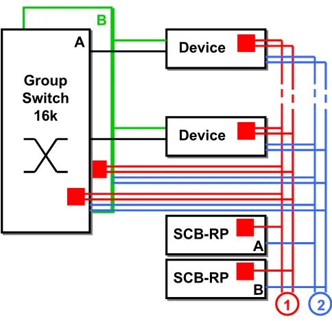
The figure below shows the control structure inside the subrack as well as the Ethernet connection which can be used by future applications. The boxes inside the boards represents the new regional processors which are integrated on the board, the RPI.
Device
Group Switch
16k A
B
Device
SCB-RP A
SCB-RP B
1
1 22 Figure 4- 4 The control structure inside GEM
The bus with number 1 is a duplicated serial RP bus in the backplane of the GEM subrack. The RP bus terminates in the RP Handler subrack of the Central Processor. The bus with number 2 in the figure is the duplicated 100 Mbit/s Ethernet bus which will be used by future applications. The SCB-RP has an Ethernet switch as well as one 1Gbit/s and one 100 Mbit/s Ethernet interface to the front of the board. It will be used by future functions in AXE.
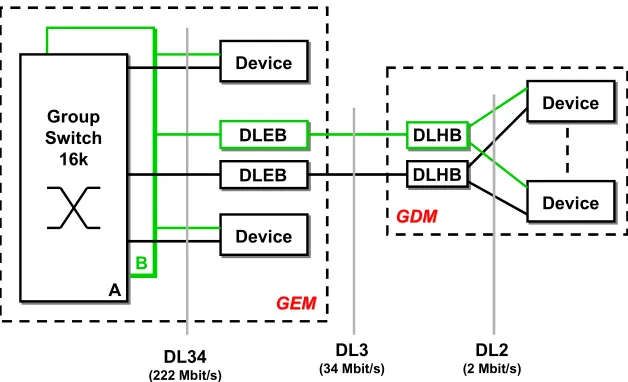
CONNECTION OF GDM
group switch in APT HWM 1.3 and 1.4. The figure below shows the main principles.
Device
DL34
(222 Mbit/s)
Group Switch 16k
A
B
Device DLEB
DLEB
Device
Device DLHB
DLHB
DL3
(34 Mbit/s)
DL2
(2 Mbit/s)
GEM
GEM
GDM
GDM
Figure 4- 5 Connection of GDM subracks to GEM
DLEB stands for “Digital Link multiplexer for Existing
equipment Board” and DLHB stands for Digital Link Handling Board. Each DLEB board can connect up to 4 DLHB boards (up to 4 GDM subracks) and there is always a need for two DLEB board; one for each plane in the group switch.
RESTRICTIONS
THE NEW GROUP SWITCH
GENERAL
The new group switch in AXE 810, which is referred to as GS890, is a completely new switch. In earlier AXE
modernisations, the group switch structure has been the same but the hardware has been modified and extended to 128K. This time, the group switch is new. The main features are:
• Distributed architecture
The switch is located in every GEM subrack as indicated earlier in this book.
• Time-Space architecture
The old AXE group switch had a time-space-time (TST) architecture. This new one has a time-space (TS)
architecture creating better characteristics. • Maximum size of 512K
The switch can be scaled up to 512K multiple positions (64 kbit/s channels). This means that the switch can have more than 250 000 calls established at the same time
(theoretically).
• Subrate switch up to 128K
The size of the subrate switch can be extended up to 128K. The subrate is used in mobile applications. The
implementation of the subrate switch differs from earlier GS hardware.
• Strictly non-blocking
The old group switch in AXE was not strictly non-blocking as each inlet could be loaded to about 80%. The new architecture with time-space structure gives this advantage. • Reduced cabling
The cabling has been reduced to about 1/12 if compared with the old switch (GS12).
• Reduced power consumption
The power consumption has been reduced to 1/6 of the old switch’s power consumption for the same switch size (GS12).
• Reduced space
• Device protection without waste of multiple positions For ET155, protection switching is an option. In that case, the interface to the group switch can connect two ET155:s without wasting multiple positions.
The architecture of the switch is further described in the following chapters.
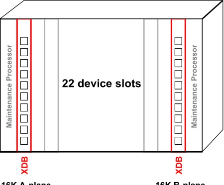
HARDWARE
The main hardware when it comes to switching is the XDB board (X means switching and DB stands for “distributed board”). The XDB boards has a switching capacity of 16K and there are two in each GEM subrack, one for the A-plane and one for the B-plane.
Ma in te na nc e P roc e ss o r 16K B-plane 16K A-plane XD B Ma in te na nc e P roc e ss o r
22 device slots
XD
B
Figure 4- 6 The XDB boards in GEM
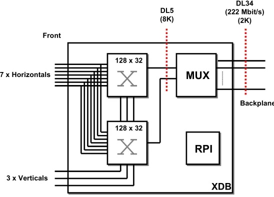
On the XDB board, there are three ASICs (application specific integrated circuit) which implements the 16K switch. One ASIC is a multiplexer and two are holding the speech stores (SS) and control stores (CS). One integrated Regional Processor (RPI) is also on the XDB board. The devices in the subrack are
connected to the XDB boards via the backplane while
MUX
128 x 32
Backplane Front
RPI
DL34 (222 Mbit/s)
(2K) DL5
(8K)
128 x 32
7 x Horizontals
3 x Verticals
XDB
Figure 4- 7 Circuits on the XDB board
The structure of the switch is explained in next chapter.
STRUCTURE
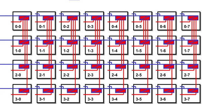
If you only have a 16K group switch, it is enough to have just one XDB circuit board. However, in case of larger switches, the XDB boards have to be inter-connected by means of so-called horizontal and vertical connections. The horizontal and vertical connections are best explained if you imagine all XDB boards put in a matrix. The figure below shows the main idea.
0-0 0-1 0-2 0-3 0-4 0-5 0-6 0-7
1-0 1-1 1-2 1-3 1-4 1-5 1-6 1-7
2-0 2-1 2-2 2-3 2-4 2-5 2-6 2-7
3-0 3-1 3-2 3-3 3-4 3-5 3-6 3-7
Figure 4- 8 A matrix of switch boards.
Each board has a capacity of 16K so the maximum capacity in the switch is 4 rows x 8 columns x 16K = 32 x 16 = 512K.
Horizontals and Verticals
• Horizontals
These connections connect all switch boards in a row to each other. The connection is “all to all” meaning that all boards in a row have direct connections to all other boards in the same row.
• Verticals
These connections connect all switch boards in a column to each other. Also these connections are “all to all”.
Showing all cables from all switch boards in a 512K switch is difficult but the figure shows all the cabling going to and from the first board (0-0) in the switch matrix.
0-0 0-1 0-2 0-3 0-4 0-5 0-6 0-7
1-0 1-1 1-2 1-3 1-4 1-5 1-6 1-7
2-0 2-1 2-2 2-3 2-4 2-5 2-6 2-7
3-0 3-1 3-2 3-3 3-4 3-5 3-6 3-7
Horizontals
Verticals
Figure 4- 9 Cabling from one switch board (note that all cables are not shown in the figure)
The Switching
0-0 0-1 0-2 0-3 0-4 0-5 0-6 0-7
1-0 1-1 1-2 1-3 1-4 1-5 1-6 1-7
2-0 2-1 2-2 2-3 2-4 2-5 2-6 2-7
3-0 3-1 3-2 3-3 3-4 3-5 3-6 3-7
Speech Store and Multiplexer
Figure 4- 10 A switch matrix with horizontals and verticals (simplified, as verticals are only shown from row 0)
The principle of switching is as follows:
1. A speech sample comes in on a horizontal and is then copied to all speech stores on that row. The horizontals takes care of that.
2. The time switching takes place in the speech store of the correct column and the speech sample is sent on the vertical to the correct board.
3. On the destination board, a multiplexer takes the correct speech sample from the vertical.
The switching in the other direction works according to the same principle but that will take another path. The figure below shows the main principle of switching between two switch boards in a part of the switch.
0-0 0-1 0-2 0-3
1-0 1-1 1-2 1-3
2-0 2-1 2-2 2-3
3-0 3-1 3-2 3-3
Figure 4- 11 Switching in both directions.
It can be seen that the samples take different paths. The rule is always to copy the speech sample to all speech stores on the same horizontal (in the same row) and then switch to the correct vertical.
Subrate
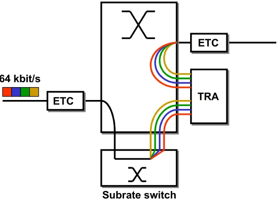
Subrate is used in mobile applications (for example in the BSC in GSM) to allow one 64 kbit/s channel to include more than one call. For example, most mobile systems code speech to less than 8 kbit/s which means that one 64 kbit/s channel can send 8 calls. To be able to switch these sub-rate channels, the group switch must be designed in a special way.
In the “old” group switches, the subrate switch was a “back pack” solution with a special subrack implementing the switch. The maximum capacity was 4K in all earlier version of AXE. The figure below shows the main principle of the old subrate solution.
ETC 64 kbit/s
Subrate switch
TRA ETC
Figure 4- 12 Subrate in the old group switch
0-0 0-1 0-2 0-3 0-4 0-5 0-6 0-7
1-0 1-1 1-2 1-3 1-4 1-5 1-6 1-7
2-0 2-1 2-2 2-3 2-4 2-5 2-6 2-7
3-0 3-1 3-2 3-3 3-4 3-5 3-6 3-7
Figure 4- 13 Subrate can only be used in the first row of the group switch.
Wideband
Wideband means that the group switch hardware can be used to set-up several 64 kbit/s channels that are kept together. For example, an ISDN subscriber using both B channels for internet access, must have 2 x 64 kbit/s switched though the exchange. The new GS890 can handle wideband in the same way as previous switches; it can establish up to 31 x 64 kbit/s through the switching hardware with the order kept of the channels.
Modularity
The switch has two main limitations when it comes to how it can be built:
• The subrate part must be in the first row. One row has the capacity of 128K which is the maximum capacity of the subrate switch.
• All rows and all columns must be of same length. This has to do with the switching principle explained in the previous chapter.
0-0 0-1 0-2 0-3 0-4 0-5 0-6 0-7
1-0 1-1 1-2 1-3 1-4 1-5 1-6 1-7
2-0 2-1 2-2 2-3 2-4 2-5 2-6 2-7
3-0 3-1 3-2 3-3 3-4 3-5 3-6 3-7
32K with 32K subrate
Subrate
128K no subrate
320K no subrate
Figure 4- 14 Switch sizes, examples
Please note that the extension must create a rectangle because of the switching principle. As an example, if you have a 128K switch as in the figure above, it is not possible to just add one 16K switch (2-0 or 0-4). One column or one row must be added.
Reliability
Just as with previous group switches from Ericsson, the whole switch is duplicated. The two parts are referred to as A-plane and B-plane. Each device is connected to both planes and the system will not be disturbed for single hardware faults.
SYNCHRONISATION
Group Switch A B CLM (CGB, Clock Generation Board) CLM (CGB, Clock Generation Board)
Figure 4- 15 Clock Modules provide timing information
External synchronisation of a node in a network must be
possible in different ways. The exchange clock system in CL890 supports the following:
• A local reference clock in case of interrupt of external timing information. The function is referred to as Reference Clock Module (RCM) and the hardware is called Local Reference Board (LRB). This gives better long-term stability that just having the CLMs.
• External references from incoming PCM lines or external sources from other vendors. These references are connected via one or two Incoming Reference Board (IRB) which converts the incoming source to 8 kHz.
• Stand alone clocks like the Ericsson Central Building Clock (CBC) or the GPS System Clock (GSC).
The figure below gives a summary of the different alternatives.
Switch core Plane A and Plane B 8 kHz CLM (CGB-0) CLM (CGB-1) RCM (LRB) ICF (IRB) Stand alone clock (CBC or GSC) MV MV 2 Mbit/s GPS ETC, ET155, RCM or Stand alone clocks
Depending of the planned maximum size of the group switch, different configuration alternatives exist for the clocks. The three following alternatives exist:
1. Clocks for a GS consisting of one GEM (16k)
In this case, everything can be housed in the same GEM subrack. The subrack could lock like the example below.
XDB IRB XDB
CG B-0
CG B-1 IRB SC
B-RP
SC B-RP
8 device slots 8 device slots
Figure 4- 17 Clocks for one GEM
2. Clocks for a GS built with 8 GEMs (128k)
Two of the GEMs have a CGB board, one IRB board and two CDB boards for distribution of timing information. Please study the example below. All other GEMs (1-6) only have the XDB boards as the cables terminate in these boards.
XDB IRB XDB
CG B-0
CDB SC
B-RP
SC B-RP
8 device slots 9 device slots
CDB
Figure 4- 18 Clocks for GS up to 128k
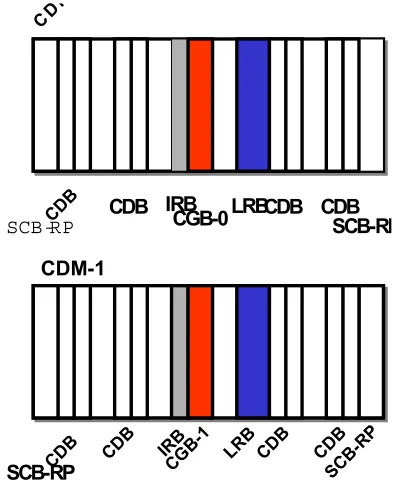
3. Clocks for a GS built with 32 GEMs (512k)
SCB-RP
CDM
CDB CDB IRBCGB-0LRBCDB CDBSCB-RP
SCB-RP CDM-1
CDB CD B
CDB CDB SC
B-RP IRB
CG B-1
LRB
Figure 4- 19 Clocks for GS up to 512k
CABLING
Cabling from XDB boards
It has already been mentioned that an XDB board (the switch in the GEM subrack) is connected to both horizontals and verticals. By studying the front of the board, that is quite easy to see as there are 3 vertical connections and 7 horizontal connections. The board also has 2 connectors for connection of clocks (timing information from CLMs). The figure below shows the front of the XDB board.
XDB
3 Vertical Connections
7 Horizontal Connections
2 Connections from clocks
1 2 3 4 5 6 7 1 2 3
Cabling for clocks
The cabling from the clocks to the XDB boards, and also
between the two CGB boards, is slightly more complicated. The main reason is that there are many different alternatives
depending on expected maximum size of the group switch (i.e. the number of GEM subracks. The example in this book will be a group switch with a size between 32K and 128K (2-8 GEM subracks). If the switch is larger than 128K, two separate subracks will be used for the clocks (as described earlier).
The example has three GEM subracks where there is only clock module in each one of the two first. In these two subracks, there are two clock distribution boards as well (CDB). The figure below shows the principle of the cabling with 3 GEM subracks.
X D B
CG
B
-0
GEM-0
CDB XD
B
CDB
XD
B
CG
B
-1
CDB XD
B
CDB
XD
B
XD
B
GEM-2
GEM-1
SINGLE-BOARD ET155
ET155 is not new in that sense that it existed also in APT 1.4. However, the ET155 released in AXE 810 is a single board solution which reduces footprint and power consumption considerably. The same board may be used for all three main transport standards: ITU, SONET and TTC standards
(European, American and Japanese standards). By having one single board for the 155 Mbit/s interface gives a number of advantages to the customers:
• Simplified connection to the transport network due to large savings in cabling and DDF (if compared with the use of 2 Mbit/s interfaces).
• reduced footprint
• reduced power consumption • reduced cabling
• simplified handing.
The table below makes a comparison between the versions available in AXE Classic, HWM 1.3 and HWM 1.4 and the new single board ET155. Please note that the comparison is made with the European version (E1) and that the savings in footprint and power consumption is even larger if compared with the US or Japanese versions (T1/J1).
ETC in BYB 202 (2 Mbit/s)
ETC in BYB 501, 1.3 (2 Mbit/s)
ETC in BYB 501, 1.4 (155 Mbit/s)
Single board ET155
Footprint ~160 ~ 44 4.5 1
Power Consumption
- - 5 1
Number of
boards Multiplexer63 + RP + Multiplexer63 + RP + 5 to 6 1 Cost for large
DDF Yes Yes No, but smallODF No, but smallODF
Figure 4- 22 The new single-board ET155 compared with older versions
ETC51
DDF
SDH Transport
Network ETC563
Terminal or Add/drop Multiplexer
Figure 4- 23 Connection of AXE with E1 links
If the same capacity is needed but an ET155 is used instead, the picture is much simpler. The figure below shows the situation.
ET155
ODF
SDH Transport
Network
Figure 4- 24 Connection of AXE with the new ET155
The number of exchange terminals is reduced if using ET155 instead of the old ETC5 having a 2 Mbit/s interface. If
upgrading from AXE HWM 1.4 to the new hardware, also there a significant saving can be achieved. Please study the figure below.
LO T-w LO T-w LO T-w LO T-w
Working
LOT-p
HOT-p HOT-w
Protection
ET155-7
ET155-w
ET155-p
Working
Protection DL3
DL34
Figure 4- 26 Protection function
The list of functions in ET155 is quite long. To summarise it, please look at the list below.
•
155 Mbit/s SONET termination in accordance with ANSI standards OC3 IR-1,ANSI T1105.06-1996; 1310 nm• 155 Mbit/s SDH termination in accordance with ETSI, ITU-T, ANSI and TTC standards
• Automatic Protection Switching (APS), option • Hardware inventory support
• Audible tone sending and attenuation on 64 kbit/s channels • MTBF > 25 years
TRANSCODERS, TRA
POSITION OF TRA
Transcoders are used in mobile systems to change the coding from the ordinary PCM coding with 64 kbit/s to a lower bit rate. The main reason for changing the coding is that PCM is not well suited for radio transmission due to high bit rate and no
functions for handling transmission errors often occurring on the radio path. The transcoders are located in the Base Station Controller in GSM. The figure below shows the position of the transcoder in the system.
Figure 4- 27 The position of the transcoders in mobile systems
THE FUNCTION OF THE TRA
As already described is one of the main problems with mobile communication the bad radio connection. This requires a special coding format for the speech in order to reduce number of bit/s and to increase speech quality. The job of the transcoder is to convert between different coding standards. The coding
standards used in the fixed part of the mobile network is always 64 kbit/s PCM. However, in the mobile interface, there are a number of standards. To give an example, we can study GSM which today has three different coding standards defined:
• Full Rate (FR)
This was the first coding standard in GSM and it codes speech with 13 kbit/s.
• Enhanced Full Rate (EFR)
This coding format gives better speech quality but with maintained bit rate of 13 kbit/s. The algorithm demands more processing power.
• Half Rate (HR)
BSC MSC
16 or 8 kbit/s TRA 64 kbit/s PCM
64 kbit/s PCM
This means that the transcoders must be able to support a number of different speech coding algorithms at the same time. The figure below shows the main function of the transcoder.
Half Rate (6.5 kbit/s) TRA PCM (64 kbit/s)
Figure 4- 28 Main function of transcoder, TRA
The coded speech in GSM will be 6.5 kbit/s but this bit stream is put in an 8 kbit/s bit stream (1/8 PCM channel) due to the fact that the subrate works on 8 kbit/s level. Additional 1.5 kbit/s is filled with signalling and padding (rate adaptation).
THE NEW TRA HARDWARE
The new hardware for transcoders is built round a speech
processing platform called CSPB, Common Speech Proccessing Board. The capacity has been increased significantly if
compared with the previous versions. Please study the table below.
TRA R5 (GSM)
TRAB3 (TDMA)
TRA R6 (GSM)
Channels per board
24 48 192
Capacity 1 1 8
Volume 1 1 1/8
Power consumption
1 1 1/3
Figure 4- 29 Capacity of the new TRA hardware
TRA TRA TRA
ETC
ETC
BSC or MSC
ETC
ECHO CANCELLERS IN POOL, ECP
THE PROBLEM WITH ECHO
The echo canceller is a device which is connected to the speech path to remove echo caused by long delays in the speech path. Some speech energy leaks back in the analogue line circuit and returns to the sender. It is the so called “fork” in the line circuit, converting from 2-wire to 4-wire connection, which causes the leak of speech energy.
Traditionally, delay has been caused by satellite links but today, the digital mobile phones cause a delay because of the speech coding process and the way the speech is transmitted. For that reason, echo cancellers are used on a broader basis in a modern network. The figure below shows the main function of an echo canceller when a digital mobile phone is connected to an analogue telephone in the fixed network.
LIC
= Echo
Echo canceller
Figure 4- 31 The position and function of an echo canceller
Echo cancellers are also pooled, just as the transcoders, and connected to the speech path if needed. This reduces the total number of echo cancellers and it creates redundancy. Faulty echo cancellers are simply blocked and not connected. The figure below shows the main principle of pooled echo cancellers.
TRA TRA ECP
ETC
ETC
MSC or Transit Exchange
ETC
ETC ETC
ETC
THE NEW ECP HARDWARE
Also the echo cancellers are made on the common speech processing platform CSPB, Common Speech Processing Board. The ECP is, just as the transcoder, also located in the new GEM subrack and connected to the group switch via the backplane interface. The capacity has increased significantly as can be seen in the table below.
ECP 404 ECP5
Channels per
board 32 128
Capacity 1 4
Volume 1 1/4
Power consumption
1 1/2
PDSPL-2E
Some abbreviations are longer than others. This is probably one of the longest within Ericsson. The abbreviation PDSPL-2E stands for “second enhanced generation Pooled Digital Signalling Platform Loadable”. Easy…
BACKGROUND
In a telephone exchange, there are several types of devices that send tones of various types. Examples are analogue signalling devices and tones sent and received to/from subscribers. In the older versions of AXE, based on BYB 202, each type of tone sending was performed by separate devices. Some years ago, the common hardware PDSPL1 in BYB 202 was developed. Still, there where different boards for different functions.
When BYB 501 was released in 1997, the PDSPL-2H was released at the same time. This was a general hardware platform for tone sending but the boards came pre-programmed from the factory. To add new devices of a specific type, the customer had to order a PDSPL board with the correct identity (index) to get the desired functionality. The board is housed by the GDM subrack and it occupied 40 mm of space.
With the PDSPL-2E, the customer can buy a general board, which is empty when delivered from Ericsson, and then load it with the desired function. The figure below shows the evolution.
TCD on BYB 202
TCD on BYB 202 with PDSPL1
TCD on BYB 501 with PDSPL-2H
TCD on BYB 501 with PDSPL-2E
TCD SW
Figure 4- 34 Evolution of PDSPL (example of a TCD application)
The functions that are implemented in PDSPL-2E are:
• CSR, Code Sender Receiver
MFP or CCITT No 5 signalling. The signalling is made with tones. For software compatibility, one board supports 16 CSR devices.
• TCD (Transceiver Check Device) performs trunk line continuity checks.
• CAT (Code Answer and Tone Sender) is a fully
programmable sender for all sorts of maintenance tones and sequences. Through the use of commands, it is possible to define any type of tone as well as complete code answers through the linking of tones and idle/zero.
• TRU (Tone Receiving Units) is a tone receiver used by the GTT and PRT AXE functions. GTT (Generated Test Traffic) generates calls to exchanges with code answering equipment. The TRU unit detects and verifies the incoming code answers. GTT is only used in conjunction with A-law. PRT (Progression Test) is a related function that is in employed in markets where µ-law is used.
• KRD (Key-set Code Receiver Device) is used as a DTMF receiver combined with a dial-tone tone sender. KRD is capable of sending either a single tone, a sum of two tones or an amplitude modulated tone with carrier suppression. Both A- and µ-law coding is supported.
• CSKD (Code Sender Key-set Device) is used as a DTMF sender. Both A- and µ-law coding is supported.
• CSFSKD (Code Sender FSK Device, FSK meaning Frequency Shift Keying) is a sender for calling-line identification. Both A- and µ-law coding is supported. • CCD (Conference Call Device) is the hardware supporting
the Multi Junctor Function. Multi Junctor is a platform function that allows the connection of more than two participants to a call. The Multi Junctor Function supports two main functions (monitoring and multi party call) that are independent of one another. Six supplementary functions are associated with these two main functions, i.e., internal connection, speech attenuation, tone sending, speech control, comfort noise and companding law.
devices are connected to the group switch via DL2 interfaces going in the backplane of the Generic Device Magazine (GDM). The RP is the link between the PDSPL device and the Central Processor. Please study the figure below.
GDM
RP4 PDSPL DLHB GEM RPB-S
CP
Group Switch
Figure 4- 35 The PDSPL in AXE
The CP has a path to the PDSPL via the RP4 in the GDM subrack. Via the DLHB boards and the GEM subrack, the PDSPL has a path to the group switch. From the group switch, both locally connected subscribers as well as subscribers connected via incoming lines, can be served by any PDSPL within the exchange. Notice that it is not possible to mix old and new PDSPL boards within the same magazine.
HARDWARE
The hardware is build-up around a few main components:
• One device processor with RAM memory.
• One interface circuit which has EM bus interface as well as DL2 interface to the group switch. The circuit is an ASIC as both EMB and DL2 are proprietary interfaces.
• Three Digital Signalling Processors (DSP) which are connected to the DL2 interface as well as internally connected.
• A flash memory for storage of the loaded software. The contents of the flash memory is copied to the RAM memory of the processor as well as to the internal memory of the DSPs when the board is reset.
DSP 0 DSP
1 DSP
2
Flash
RAM Device
Processor
Interface
circuit (ASIC) DL2 (to/from GS) EM bus (to/from RP)
Figure 4- 36 The hardware of the PDSPL-2E board
The size of the PDSPL circuit board has been reduced to 50% compared with previous version. The functionality of the
PDSPL circuit board has not been changed but the size has been reduced. Please study Figure 4- 37 below.
P D S P L -2 H P D S P L -2 E
40 mm 20 mm
Figure 4- 37 The size has been reduced of the PDSPL circuit board
THE LOAD FUNCTION
• The PDSPL Application Loader (PDAL) function. This function makes it possible to load the PDSPL boards with firmware stored in the CP.
• The APZ 10.0 operating system or higher
It is not possible to mix loadable and not loadable PDSPL boards in the same subrack. In the exchange, it is possible to have a mix between the “old” and the new PDSPL hardware.
The PDSPL hardware can be mixed with any other type of hardware adapted for the GDM subrack. The only limit is the capacity of the RP.
The loading of firmware start by loading them into the Program Store (PS) of the central processor. The loading is done from the IOG/APG. Two software units handle the loading; one in the central processor and one in the regional processor. Please study the figure below.
APG
CP RP
PS
PDAL1U PDAL1R
PDSPL HW
RPB EMB
Figure 4- 38 Overview of the firmware loading using PDAL
The function also has two tables:
• A licence and configuration table
The table stores information about which of the applications that are free to use. This makes it possible for Ericsson to licence functions to operators. When the licence fee is paid, the application can be used by the operator in as many PDSPL boards as they wish.
• A downloaded EM table
The table stores information about firmware that has been loaded in PDSPL boards. The table is updated after successful loading of firmware.
ATM LINK INTERFACE, ALI
ATM will be used extensively in the 3:rd generation mobile system as bearer of voice and data. In the case of AXE, ATM will be used in cases where ATM is used to access the radio part of UMTS (referred to as UTRAN). Different scenarios are defined to how the future network will evolve and the figure below shows one possible scenario where an existing GSM operator adds an UTRAN network and lets his existing AXE switches interface to this network. This means that AXE needs and ATM interface that can handle voice, data and SS7
signalling.
UTRAN
ATM Connectivity
Network
ATM TDM (SDH) Step 1
Step 2
Figure 4- 39 AXE interfaces the ATM network in UTRAN
The interface is an optical 155 Mbit/s interface that supports different ATM services. Voice and data will use AAL2 while signalling uses AAL5. In the case of signalling, the ALI will include signalling parts which enables it to extract the signalling and send it to the CP for analysis. Please study the example in the figure below.
ALI
CP
ET155
155 Mbit/s ATM
#7
SDH AXE Media Gateway
Figure 4- 40 Signalling on AAL5
HDLC-based format between the ALI and the Transcoder (TRA). AAL2 is used and the ALI can in the first release handle 480 channels. Permanent Virtual Circuits (PVC) are set-up between the ALI and different end points and AAL2 signalling can be used inside these PVCs to establish and release calls (Q.AAL2 signalling). Please study the figure below.
A LI
ET155
A A L2
SD H A XE M edia G atew ay
TRA
HDLC
Figure 4- 41 The ALI is used for coded AAL2 transmission
The ALI can also handle 64 kbit/s speech on AAL2. In that cane, no TRA is need to change the coding of the speech (it is done in the UTRAN network). The ALI can in the first release handle 480 channels.
In case of circuit switched data, ATM will carry data in cells which will terminate in a so called Data Transmission Interface (DTI). This equipment is in GSM referred to as Interworking Unit (IWU). The ALI can handle 8 channels of circuit switched data. Note: 8 channels does not seem to be enough but consider that most of the data traffic in 3:rd generation mobile system will go over packet switched networks built on IP or ATM. The figure below gives an example of an ALI handling circuit switched data as well as 64 kbit/s un-coded speech.
ALI
ET155
64 kbit/s voice
AXE Media Gateway
DTI
SIGNALLING LINKS
All types of signalling links are based on the RPP and the RPG platforms. Both these processor types have been described in the APZ chapter (chapter 3) regarding performance and structure. These two following chapters will describe the protocols supported by the APT software.
SS7 SIGNALLING LINKS
All signalling links are based on the RPG3 hardware which is an improvement of the RPG2 regarding capacity. The following signalling standards are supported by the AXE 810 software.
• ITU-T C7, 64 kbit/s
The signalling terminal fulfils ITU-T Q.703 white book recommendation. One RPG3 can handle 4 signalling links for all traffic mixes.
• ANSI SS7, 64 kbit/s
The signalling terminal fulfils Bellcore GR-246-CORE. One RPG3 can handle 4 signalling links for all traffic mixes. • ANSI SS7, 56 kbit/s
The signalling terminal fulfils Bellcore GR-246-CORE. One RPG3 can handle 4 signalling links for all traffic mixes. All three signalling terminals are placed in a GDM-H subrack which can have up to 8 RPG3s. This means that one subrack can have up to 32 signalling terminals operating at 64 or 56 kbit/s.
There are also non-GS connected signalling terminals on another platform than RPG. The signalling terminals are placed in GDM2-H subracks with the possibility to have 4 signalling terminals. The three standards supported are:
• ANSI DS0A SS7, 56 kbit/s
The signalling terminal fulfils Bellcore GR-246-CORE and DS0A maintenance functionality in accordance with
Bellcore GR-OPT-000489. • ANSI V35 SS7, 56 kbit/s
The signalling terminal fulfils Bellcore GR-246-CORE. • Japanese J7X21 J7, 48 kbit/s
HIGH-SPEED SIGNALLING LINKS (HSL)
A high-speed link is used in some applications where there is high load on the signalling links. Examples are to Home Location registers (HLR) in mobile networks or to Service Control Points (SCP) for intelligent network services.
An HSL is based on a full 2 Mbit/s (or 1.5 in Japan or the US) used for signalling and the link is terminated in the RPP. This means that a HSL roughly has 30 times the capacity of an ordinary 64/56 kbit/s signalling link. The signalling is based on ATM and the ATM cells are mapped to a standard 2/1.5 Mbit/s ETC or to a tributary of and STM-1 (ET155). Please study the figure below.
R P P
E T 155 A X E
ETC
2 Mbit/s
Figure 4- 43 High-speed link for signalling
Two types of HSL standards are supported:
• HSL ETSI, 2048 kbit/s
One RPP supports one high-speed signalling link for all traffic mixes. The software supports ITU-T Q2110, 2140 and 2144. That corresponds to SSCOP, SSCF and SAAL Layer Management respectively.
• Japanese HSL, 1544 kbit/s