Article 1
Modeling and Analysis of Opto-Fluidic Sensor for
2
Lab-On- a-Chip Application
3
Venkatesha M. 1*, Chaya B. M. 1, Pattnaik P. K. 2 and Narayan K. 1 4
1 Sai Vidya Institute of Technology, Bengaluru, Karnataka, India; [email protected] 5
2 BITS-Pilani, Hyderabad campus, Hyderabad, India. 6
* Correspondence: [email protected]; Tel.: +91-897-113-7161 7
Abstract: In this work modeling and analysis of an integrated opto-fluidic sensor, with a focus on
8
achievement of single mode optical confinement and continuous flow of micro particles in the
9
microfluidic channel for Lab-on-a Chip (LOC) sensing application is presented. This sensor consists
10
of integrated optical waveguides, microfluidic channel among other integrated optical
11
components. A continuous flow of micro particles in a narrow fluidic channel is achieved by
12
maintaining the two sealed chambers at different temperatures and by maintaining a constant
13
pressure of 1Pa at the centroid of narrow fluidic channel geometry. The analysis of silicon on
14
insulator (SOI) integrated optical waveguide at an infrared wavelength of 1550nm for single mode
15
sensing operation is presented. The optical loss is found to be 0.0005719dB/cm with an effective
16
index of 2.2963. The model presented in this work can be effectively used to detect the nature of
17
micro particles and continuous monitoring of pathological parameters for sensing applications.
18
Keywords: micro fluidic channel; micro particles; fluid flow rate; lab-on-a-chip; waveguide
19 20
1. Introduction 21
A Lab-On-a-Chip (LOC) is a device that integrates many laboratory tests on a common
22
integrated circuit. The size of LOC is in the range of few millimeters to few square centimeters [1].
23
LOC’s requires the combination of microfluidics, manipulation and study of micro liters of fluids
24
and light-fluid interaction. Most of the LOC fabrication processes were developed on silicon. Silicon
25
fabrication processes are directly derived from semiconductor fabrication. The demands for cheap
26
and easy production of LOC’s results in a simple technology for the development of
27
polydimethylsiloxane (PDMS), microfluidic devices [2]. LOC’s provides application related
28
advantages such as low fluid volume consumption, faster analysis, quick response times and
29
compactness of the system due to the integration of multiple functions [3].
30
In most of the opto-fluidic sensors used in LOC applications, the sensitivity and accurate test
31
results depends on microfluidics, light-fluid interaction and light guiding properties of optical
32
waveguide. Microfluidics involves behavior, control and manipulation of fluids that are
33
geometrically constrained to a millimeter scale. At small scales (channel size around 100nm to
34
500µm), the comparison between effects of the momentum of a fluid to that of viscosity is given by
35
Reynolds number and its value can become very low. At lower Reynolds number, fluid flow
36
becomes laminar and molecular transportation occurs due to diffusion [4]. Accurate specifications
37
in chemical and physical properties such as temperature, concentration and pressure results in more
38
uniform reaction conditions and more accurate single or multi step reactions [5,6]. In this article the
39
optical waveguides and microfluidic channel are developed by using silicon as guiding medium.
40
Silicon is transparent to infrared light with wavelengths above 1100nm [7]. In the development of
41
biosensors, the bio-sample flow rate plays a very important role in its sensitivity. The sensitivity of
42
ultrasensitive and selective non-enzyme using copper wires is found to be high at near infrared
43
region [8]. Electrochemical detection of glucose from whole blood using copper wires [9], radio
44
frequency [10], and capillary based ring resonators [11] is presented with many other sensing
45
mechanisms [12-17].
46
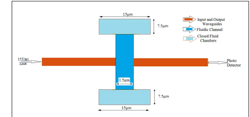
Figure 1 shows schematic of an integrated opto-fluidic biosensor employed for modeling and
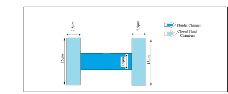
47
simulation. It consists of a laser source at 1550nm, photo detector and SOI input and output
48
waveguides (shown in Red color) with a narrow fluidic channel (Shown in blue color). In the
49
operation, the optical power is coupled into the input waveguide by using laser source (1550nm).
50
The guided modes propagate through the input waveguide and couples into the fluidic sensing
51
region. When the light couples from input waveguide to the output waveguide through the fluidic
52
sample the absorption of optical power occurs due to the properties of the micro particles present in
53
the fluidic sample. Based on the fluidic gap distance, a mode mismatch occurs between fluidic gap
54
and input waveguide. Mode mismatch occurs due to the absorption of optical power [18], in fluidic
55
gap. Hence mode mismatch which occurs during propagation of light through sensing region
56
(fluidic gap distance) and absorption of optical power by the analyte is used for the purpose of
57
analysis and also as a designing tool
58
59 60 61 62 63 64 65 66 67 68 69 70 71 72 73 74
Figure 1: Schematic representation Integrated Biosensor 75
In this article modelling of micro fluidic channel to achieve a continuous flow rate between two
76
sealed chambers maintained at different temperatures and pressure acting on the fluidic channel
77
walls is described in section two. The modelling and modal analysis of SOI waveguides for use in
78
light propagation is discussed in section three. The optical properties of SOI waveguide at infrared
79
wavelength range 1500nm to 1600nm and power coupling analysis is depicted in section four.
80
2. Modeling of Micro Fluidic Channel 81
In this section microfluidic structure shown by blue color in Figure 1 is designed and analyzed.
82
Micro fluidic channels are small dimension structures developed to achieve flow rate, sorting and
83
manipulation of fluids that are geometrically constrained.
84
Figure 2 shows the structure of micro fluidic channel used for analyzing the flow rate between
85
the two closed fluidic chambers, which are maintained at different temperatures. It consists of two
86
fluidic chambers having dimensions of 7.5µm in length and 15µm in depth. The fluidic chambers are
87
linked by a narrow channel having 1.5µm width and 15µm in length. The chamber and channel
88
walls are modeled using silicon as material having a thickness of 1µm. The walls of the two
89
chambers are in thermal contact with heat sinks maintained at 290 K and 300 K, respectively. The
channel walls are thermally insulated. The fluid in the center of the channel is maintained at a
91
pressure of 1 Pascal.
92 93 94 95 96 97 98 99 100 101 102 103
Figure 2: Structure of micro fluidic channel 104
The micro fluidic channel shown in figure 2 is used to compute the flow between two sealed
105
chambers (closed fluid chambers) connected by a micro-channel with conducting walls when the
106
chambers are maintained at different temperatures. The material used for the walls is Silicon. To
107
achieve a continuous flow rate between two sealed chambers a birefringent object is used with a
108
pressure point at the centroid of channel geometry. For channels of micron scale dimensions the
109
Knudsen number becomes larger than 0.01. At atmospheric pressure, it is therefore necessary to use
110
a slip condition on the surfaces of walls in the vicinity of the channel. The slip velocity,
u
slip, along111
the walls of the micro fluidic channel is given by equations (1) and (2) [19].
112
( )
(
)
(
)
[
T(
n. T)
n]
Tn n n n
u W W
F T T
s
slip=σ λμτ − τ +σ ρμ ∇ − ∇ (1)
113 .T . λ ζ T
TW = F− T n∇ (2)
114
Where,
λ
is the mean free path of the fluid,n
is the boundary normal,τ
is the viscous stress115
tensor,
T
Wis the wall temperature,T
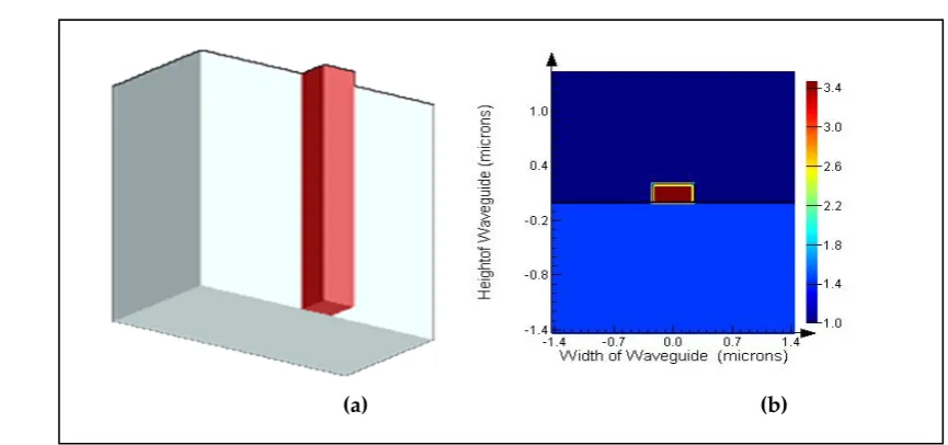
F is the temperature of the fluid,μ
is its viscosity, andρ
is116
its density. The slip coefficients,
σ
sis the viscous slip coefficient,σ
Tis the thermal slip coefficient,117
and
ζ
T is the temperature jump coefficient can be defined by material properties,a
v is the118
tangential momentum accommodation coefficient. The slip coefficients are given by equation (3), (4)
119
and (5) [20].
120 v v S a a 2− = σ (3) 121
4
3
=
Tσ
(4)122 P v v T C a a μ κ γ γ ζ 1 2 2 + − = (5) 123
Where
κ
the thermal conductivity of fluid and the mean free path can be computed from the124
fluid properties using the following equation (6) and (7) [21].
125
c C
1
O ρ
μ
λ= (6)
127
πρ
8p
πM 8RT c
n
=
= (7)
128
A continuous flow between the two sealed chambers maintained at slightly different
129
temperatures is achieved by maintaining a pressure of 1 pa at the centroid of micro fluidic geometry.
130
The channel width is 1.5µm, so the Knudsen number varies from 0.064 and 0.045.
131
The relative pressure acting on the channel wall, as a function of position along the wall is
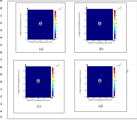
132
represented by mean path of micro particles. As the absolute pressure in a fluid flow is reduced, the
133
mean free path of the fluid molecules begins to approach the size of the vessel through, which, the
134
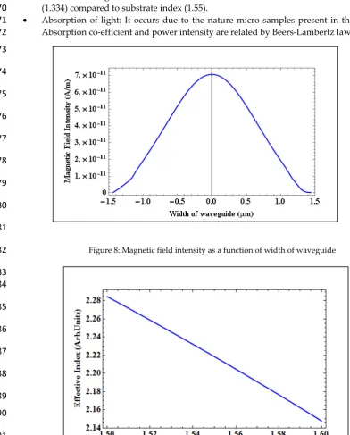
flow occurs. The detailed analysis of the velocity magnitude, Pressure and temperature analysis is
135
described in this section.
136
137
138
139
140
141
142
143
144
145
Figure 3: (a) Streamline velocity field v/s Channel length (b) Velocity Magnitude v/s Channel length 146
Figure 3 (a), shows a graph of streamline velocity field with respect to channel length. Figure 3
147
(b) shows a graph of velocity magnitude with respect to channel length. In the steady state there is
148
no net flow through the channel, but a flow parallel to the walls, in the direction of the thermal
149
gradient (cold to hot), develops due to thermal creep. In order to compensate for this flow, a back
150
flow develops in the center of the channel, which is driven by a pressure gradient in the fluid. It
151
results in a continuous flow of fluidic sample in the narrow micro fluidic channel. This is achieved
152
by maintaining a constant pressure of 1 Pascal at the center of fluidic channel.
153
Figure 4 (a), shows fluid mean free path. Such rarefied flows are characterized by a parameter
154
known as the Knudsen number, which is the ratio of the mean free path to the characteristic length
155
of the geometry. Figure 4 (b), shows the relative pressure acting on the channel wall, as a function of
156
position along the wall.
157
Figure 5 (a) and figure 5 (b) shows the temperature and pressure contours within the model. A
158
temperature jump occurs between the vessel walls and the fluid normal heat fluxes occur into the
159
wall from the fluid sample.
160
161
162
163
164
165
166
167
168
169
Figure 4: (a) Mean free path v/s Channel length (b) Pressure along channel length v/s Arc length
170
171
172
173
174
175
176
177
178
179
Figure 5: Contour diagram of (a) Temperature v/s Channel length (b) Pressure v/s Channel length 180
3. Modeling of SOI waveguide 181
In this section, the design and modal analysis of a single mode SOI waveguide structure to
182
operate at a wavelength of 1550nm is presented. The SOI waveguide is designed at infrared region
183
of light spectrum (1500nm-1600nm) for single mode operation.
184
Figure 6(a) shows the geometrical details of a SOI waveguide. It consists of silicon core having
185
dimensions of 500nm width and 250nm height. These dimensions results in single mode operation.
186
The substrate is silicon-di-oxide (SiO2), which acts as lower cladding layer for the waveguide. The
187
substrate height is designed for 2µm and width is designed for 4µm.
188
The dimensions and refractive index of the materials used in the waveguide geometry is shown
189
in table1.
190
(a)
(b)
191
192
193
194
195
196
197
198
199
200
Figure 6: (a) Waveguide geometry (b) Refractive index distribution 201
Table 1: Materials and dimensions of waveguide 202
203
204
205
206
Figure 6 (b) shows the refractive index distribution of SOI waveguide (substrate (SiO2), Core
207
(Silicon) and Cover layer (Air)) at 1550nm.. There is a high refractive index contrast between silicon
208
core (3.3714) and oxide substrate (1.55) index as well as cover layer (air) index. This high refractive
209
index contrast results in SOI waveguides being highly amenable to light guiding at infrared
210
wavelength. This results in excellent propagation characteristics such as dispersion, loss, effective
211
index. The light confinement for various wavelengths in the range 1500nm to 1600nm is depicted in
212
figure 7. It is observed that for all these wavelength range single mode operation is achieved with
213
almost negligible loss.
214
Eigen mode (EM) solver is used for numerically simulate the waveguide geometry which is
215
shown in figure. 6(a). The simulation settings used in the EM solver is shown in Table 2. Perfectly
216
matched layers (PML) boundary conditions are used in the simulation [13].
217
Table 2: Eigen Mode Solver Settings 218
219
220
221
222
223
224
Material Width (nm) Height (nm) Refractive Index at 1550nm
Si (Core) 500 250 3.4714
SiO2 (Substrate) 4000 2000 1.55
Parameter Value
Mesh Resolution 50×50
Wavelength 1550nm-1600nm
Boundary conditions PML
Background index 1 (Air)
4. Results and Discussion 225
In this section, the modal and power coupling analysis of opto fluidic sensor shown in figure 1
226
is presented. The sensor is designed to operate at 1550nm. It is observed that for 1500nm to 1600nm
227
wavelength range single mode operation is achieved with excellent optical parameters and light
228
confinement in input and output waveguides.
229
Figure 7 shows the optical mode confinement in SOI waveguide at 1550nm, 1530nm, 1550nm and
230
1600nm respectively. It is evident that the optical confinement of light is pronounced at the core of
231
the waveguide (red color) when compared to the optical power leakage into the cladding (yellowish
232
green color).Single mode operation is achieved for a core height of 250nm for the wavelength range
233
1500nm to 1600nm. In operation for bio-sensing application 1550nm is selected for the analysis.
234
Figure 8 shows the magnetic field (H-field) intensity of SOI waveguide which is confined within the
235
core region of waveguide. With the help of Figure 8, mode field diameter (MFD) is found out to be
236
1.774µm for a width of 0.5µm. Since MFD and width of the waveguide are of similar dimensions
237
indicating very good optical mode confinement.
238
239
240
241
242
243
244
245
246
247
248
249
250
251
252
253
254
255
Figure 7: Mode Confinement Plots: TE0 mode confinement in a SOI waveguide at (a) 1500nm (b) 256
1530nm (c) 1550nm (d) 1560nm 257
Figure 9 and 10 shows the effective index and loss in SOI waveguide for a wavelength range of
258
1550nm to 1600nm. Table 3 gives the effective index, loss in dB/cm, percentage of TE/TM fraction for
259
(b)
(c)
(d)
(a)
(b)
the wavelengths 1550nm, 1530nm, 1550nm and 1600nm. Light and fluidic interaction is analyzed by
260
considering fluidic region index as 1.334 (this approximately is refractive index of blood). The
261
fluidic gap distance is designed is section 2 for 1.5µm. The input waveguide is excited by a laser
262
source of 1550nm wavelength with 10dBm power level. The laser input power is coupled into the
263
input waveguide the guided modes propagates through it and interacts with fluidic sample.
264
Reflection of light takes place at the boundary between silicon core and fluidic sample. As a result
265
the change in effective index occurs and the speed at which light propagates in the fluidic sample.
266
This also results in variation of optical power intensity in the sensing region. Most of the light
267
intensity is lost in the sensing region due to following optical phenomenons.
268
• Reflections of light into the substrate: It occurs due to low refractive index of fluidic sample
269
(1.334) compared to substrate index (1.55).
270
• Absorption of light: It occurs due to the nature micro samples present in the fluidic sample.
271
Absorption co-efficient and power intensity are related by Beers-Lambertz law [19].
272
273
274
275
276
277
278
279
280
281
Figure 8: Magnetic field intensity as a function of width of waveguide 282
283 284
285
286
287
288
289
290
291
292
294
295
296
297
298
299
300
Figure 10: Loss in waveguide as a function of wavelength 301
Table 3: SOI Waveguide Parameter 302
303
304
305
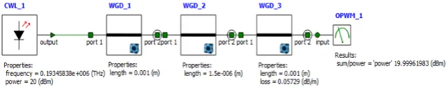
The entire Lab-on-a-Chip structure as described in schematic representation of figure 1 and
306
been simulated for optical mode propagation using 1550 nm source is shown in Figure 11. The
307
optical power measurement analysis is carried out by considering input waveguide, output
308
waveguide as mode waveguides with effective index 2.2963 and micro fluidic channel region as
309
modal waveguide with effective index 1.383. The length of input and output waveguides is selected
310
as 1mm and gap distance (fluidic channel width) is 1.5µm. The laser source wavelength is selected at
311
1550nm with a power level of 20dBm (1mW). The optical power of 19.999619 dBm is measured at the
312
end of output waveguide using optical power meter. It indicates there is significant level of optical
313
power coupling from input waveguide to output waveguide through the fluidic gap region. The
314
optimum design parameters of the proposed sensor are listed in table 4.
315 316 317
318
319
Figure 11: Optical power measurement using Interconnect 320
Table 4: Design parameters of opto-fluidic sensor 321
322
323
324
325
326
Wavelength in nm Effective Index Loss in dB/cm %( TE/TM) Fraction
1500 2.3619 0.000569 73.96/81.6
1530 2.322 0.00057 72.97/81.43
1550 2.2963 0.0005719 72.32/81.33
1600 2.230 0.00048597 70.75/81.1
Parameter Value wavelength 1550nm
Height of input/output waveguide 250nm
Width of input /output waveguide 500nm
Width of fluidic channel 1.5µm
Length of input/output waveguide 1mm
5. Conclusions 327
In this work modeling and analysis of integrated waveguides, and micro-fluidic channel for
328
opto-fluidic lab-on-chip sensor application has been presented. The flow rate analysis between two
329
fluidic chambers connected by a narrow micro fluidic channel which is in a plane perpendicular to
330
integrated optical SOI waveguides is presented. The narrow fluidic channel sandwiched between
331
two single SOI waveguides acts as a sensing region. A continuous flow of fluidic sample in the
332
narrow micro fluidic channel is achieved by maintaining pressure of 1 Pascal at the centroid of the
333
fluid channel geometry. The sensor is designed for single mode operation, which, is achieved at 1550
334
nm for waveguide dimensions of 250 nm (height) and 500 nm (width). The effective refractive index
335
was found out to be 2.2963 with a negligible loss of 0.0005719dB/cm. It is observed that, when the
336
input waveguide is excited by a laser source with 20dBm power at 1550nm, a power level of
337
19.999dBm is measured at the end of output waveguide. The power measured from output
338
waveguide gives the qualitative measurement of optical properties and nature of the micro particles
339
present in the fluidic sample. This micro structure fluidic channel with integrated laser and detector
340
can be used for Bio-sensing applications.
341
Acknowledgments: The authors would like to thank Science and Engineering Research Board, Department of 342
Science and Technology (DST-SERB) Grant Number YSS/2015/000382, Government of India for funding this 343
research work. 344
Author Contributions: “Venkatesha M, Chaya B M and Narayan K conceived and designed the experiments; 345
Venkatesha M performed the experiments; Venkatesha M, Narayan K, Chaya B M and Pattnaik P K analyzed 346
the data; Narayan K contributed analysis tools; Venkatesha M and Narayan K wrote the paper.” 347
Conflicts of Interest: The authors declare no conflicts of interest. 348
References 349
1. Volpatti L R, Yestisen A K, Commercialization of microfluidic devices, Trends in Biotechnology, 32(7), 350
347-350, 2014. 351
2. Saggiomo V, Velders H A,Sample 3D printed scaffold removal method for the fabrication of intricate 352
microfluidic devices, Advanced Science, 2(8), 2015. 353
3. Ghallab Y, Badway W, Sensing methods for di-electrophoresis phenomenon from bulky instruments to lab 354
on a chip, IEEE circuits and Systems Magazine, 4(3), 5-15, ISSN 1531-636X. 355
4. Ryan S Pawell, David W Inglis, Tracie J. Barber, and Robert A taylor, Manufacturing and wetting low cost 356
microfluidic cell separation devices, Microfluidics, 7, 2013. 357
5. Tabeling P, Introduction to Microfluidics, Oxford University Press, 2015. 358
6. Chokkalingam V, Weidonhoff B, Kraener M, Maier W F, Herminghaus S, Seemann R, Optimized drop let- 359
based microfluidics scheme for sol-gel reaction, Lab Chip, 10,2010. 360
7. Yuchan Zhang, Liang Su, Dan Manuzzi, Honorio Valdés Espinosa de los Monteros, Wenzhao Jia, Danqun 361
Huo, Changjun Hou, Yu Lei, Ultrasensitive and selective non-enzymatic glucose detection using copper 362
nanowires, In Biosensors and Bioelectronics, Volume 31, Issue 1, 2012, Pages 426-432, ISSN 0956-5663, 363
https://doi.org/10.1016/j.bios.2011.11.006. 364
8. Alejandra Fernández-Cid, Alberto Riera, Pilar Herrero, Fernando Moreno, Glucose levels regulate the 365
nucleo-mitochondrial distribution of Mig2, In Mitochondrion, Volume 12, Issue 3, 2012, Pages 370-380, 366
ISSN 1567-7249, https://doi.org/10.1016/j.mito.2012.02.001. 367
9. Julaluk Noiphung, Temsiri Songjaroen, Wijitar Dungchai, Charles S. Henry, Orawon Chailapakul, Wanida 368
Laiwattanapaisal, Electrochemical detection of glucose from whole blood using paper-based microfluidic 369
devices, In Analytica Chimica Acta, Volume 788, 2013, Pages 39-45, ISSN 0003-2670, 370
https://doi.org/10.1016/j.aca.2013.06.021. 371
10. Hyunggoo Park, Hyung Seo Yoon, Umakant Patil, Rani Anoop, Juho Lee, Juhwan Lim, Woonhyoung 372
Lee, Seong Chan Jun, Radio frequency based label-free detection of glucose, In Biosensors and 373
Bioelectronics, Volume 54, 2014, Pages 141-145, ISSN 0956-5663, https://doi.org/10.1016/j.bios.2013.10.053. 374
11. Yunhan Luo, Xiaolong Chen, Mengyun Xu, Zhe Chen, Xudong Fan, Optofluidic glucose detection by 375
capillary-based ring resonators, In Optics & Laser Technology, Volume 56, 2014, Pages 12-14, ISSN 376
12. Fernando Guerrero-Romero, Luis E. Simental-Mendía, Martha Rodríguez-Morán, Association of 378
C-reactive protein Levels with Fasting and Postload Glucose Levels According to Glucose Tolerance 379
Status, In Archives of Medical Research, Volume 45, Issue 1, 2014, Pages 70-75, ISSN 0188-4409, 380
https://doi.org/10.1016/j.arcmed.2013.11.004. 381
13. A.L. Galant, R.C. Kaufman, J.D. Wilson, Glucose: Detection and analysis, In Food Chemistry, Volume 188, 382
2015, Pages 149-160, ISSN 0308-8146, https://doi.org/10.1016/j.foodchem.2015.04.071. 383
14. Chengcheng Liu, Yongjie Sheng, Yanhong Sun, Junkui Feng, Shijin Wang, Jin Zhang, Jiacui Xu, Dazhi 384
Jiang, A glucose oxidase-coupled DNAzyme sensor for glucose detection in tears and saliva, In Biosensors 385
and Bioelectronics, Volume 70, 2015, Pages 455-461, ISSN 0956-5663, 386
https://doi.org/10.1016/j.bios.2015.03.070. 387
15. N.Y. Kim, R. Dhakal, K.K. Adhikari, E.S. Kim, C. Wang, A reusable robust radio frequency biosensor using 388
microwave resonator by integrated passive device technology for quantitative detection of glucose level, 389
In Biosensors and Bioelectronics, Volume 67, 2015, Pages 687-693, ISSN 0956-5663, 390
https://doi.org/10.1016/j.bios.2014.10.021. 391
16. Guangran Ma, Min Yang, Chenyi Li, Haiyan Tan, Liang Deng, Shi Xie, Fugang Xu, Li Wang, Yonghai 392
Song, Preparation of spinel nickel-cobalt oxide nanowrinkles/reduced graphene oxide hybrid for 393
nonenzymatic glucose detection at physiological level, In Electrochimica Acta, Volume 220, 2016, Pages 394
545-553, ISSN 0013-4686, https://doi.org/10.1016/j.electacta.2016.10.163. 395
17. Wei Shen, Jun Sun, Jowy Yi Hoong Seah, Lei Shi, Sheng Tang, Hian Kee Lee, Needle-based sampling 396
coupled with colorimetric reaction catalyzed by layered double hydroxide peroxidase mimic for rapid 397
detection of the change of d-glucose levels with time in bananas, Analytica Chimica Acta, Available online 398
9 November 2017, ISSN 0003-2670, https://doi.org/10.1016/j.aca.2017.11.003. 399
18. Narayan. K, T. Srinivas, G. Mohan Rao and M. Manoj Varma, " Analysis of integrated optical 400
lab-on-a-chip sensor based on refractive index and absorbance sensing”, IEEE sensors J, 2013,13, (5) , pp. 401
1730-1741. 402
19. Berenger, J. A perfectly matched layer for the absorption of electromagnetic waves. J. Comput. Phys.1994, 403
114, 185–200. 404
20. E.H. Kennard, Kinetic Theory of Fluides, McGraw-Hill, New York, 1938. 405
21. J.C. Maxwell, “On Stresses in Rarefied Fluides Arising from Inequalities of Temperature,” Phil. Trans. R. 406