A Broadband High-Efficiency Rectifier Based on Two-Level
Impedance Match Network
Ling-Feng Li1, Xue-Xia Yang1, 2, *, and Er-Jia Liu1
Abstract—A broadband high-efficiency rectifier with shunt-diode circuit topological structure is presented in this paper. By utilizing the two-level impedance match network, the rectifier can achieve a high microwave-direct current (mw-dc) conversion efficiency within a broad range of operation bandwidth. A stepped microstrip line and a cross-shaped microstrip stub as two-level match network is designed to extend the operation bandwidth. A cross-shaped stub connected to the capacitances act as a dc-pass filter to block the fundamental frequency wave and the high order harmonics and further improve mw-dc efficiency within a broad bandwidth. Experimental results show that the peak conversion efficiency is 80.3% at the frequency of 1.9 GHz when the input power is 22 dBm. When the input power is 19.5 dBm, the bandwidth of efficiency higher than 70% is 40% (1.80 GHz–2.72 GHz). This rectifier has the characteristics of low profile and easy integration, which is suitable for RFIDs, WSNs, and other applications.
1. INTRODUCTION
With the continuous development of microwave technology, Microwave Power Transmission (MPT) has attracted lots of attention as the power supply of Wireless Sensor Network (WSN) [1], Medical Equipment [2], Intelligent Wearable Devices [3] and Radio Frequency Identification Devices (RFID) [4]. The MPT system removes the cables and batteries, which can extend device’s lifetime and application fields. The microwave rectifier is the key component of a MPT system. It transfers microwave to dc power and provides it to the electronic equipment. The microwave to direct current (mw-dc) efficiency is the most essential parameter of a rectifier.
Recent research on rectifiers reveals that the general conversion efficiency of mw-dc is about 80% if the operation frequency is not higher than C band. However, rectifiers can only have high mw-dc efficiency above 70% at a narrow band [5, 6]. The manufacture errors may cause the variation of the operation frequency, which degrades rectifier performance, especially when the rectifier is integrated with narrow-band antenna [5, 6]. In order to meet the frequency demands of applications, a broadband high-efficiency rectifier is expected.
In order to design a broadband high-efficiency rectifier, some rectifiers using broadband match network were proposed [7–9]. A broadband match network based on grounded coplanar waveguide (GCPW) was designed to extend bandwidth [7]. The bandwidth of efficiencies higher than 50% was 54.5% (1.6 GHz–2.8 GHz). In [8], the rectifier with a high-impedance inductor achieved the efficiency of 40% over a broad frequency band from 40 MHz to 4750 MHz. A broadband rectifier reported in [9] was designed by using three section stepped impedance transformers, the rectifier covered the band from 1.65 GHz to 3.05 GHz and the maximum conversion efficiency was 78.3%. However, the efficiency over the bandwidth only reached about 50%, which cannot achieve high efficiency over the bandwidth.
Received 30 October 2017, Accepted 2 December 2017, Scheduled 13 January 2018
* Corresponding author: Xue-Xia Yang ([email protected]).
1 School of Communication and Information Engineering, Shanghai University, Shanghai 200072, China. 2 Key Laboratory of
Reference [10] reported a rectifier based on high quality factor, the bandwidth of efficiencies higher than 70% was 18.6% (1.46 GHz–1.76 GHz). The rectifier reported in [11] obtained the efficiency of 70% over a broad frequency band from 5.2 GHz to 6 GHz. However, these simple match network structures can’t extend the operation bandwidth observably and the peak efficiency decreased. In [12], the rectifier based on branch-line coupler obtained the efficiency of 70% over a broad frequency band from 2.08 GHz to 2.58 GHz. But the circuit was complex, which increased the circuit size and the processing difficulty. In this paper, a broadband high-efficiency rectifier with two-level match network is presented. This rectifier covers seven wireless communication systems of TD-SCDMA, CDMA2000, TD-LTE, FDD-LTE, UMTS-2100, Wi-Fi and Bluetooth. By using the two-level impedance match network, the proposed rectifier achieves high mw-dc efficiency within a broad bandwidth. A dc-pass filter is designed to block the fundamental frequency wave and the high order harmonics within a broad bandwidth. The rectifier has the characteristics of simple structure and easy integration, which can be applied as the power supply of WSN and RFID systems.
2. THE DESIGN AND SIMULATION OF RECTIFIER
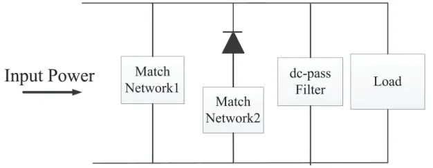
Figure 1 shows the basic topological structure of this rectifier. The circuit is based on diode-shunt topological structure, which is composed of a two-level match network, a packaged diode, a dc-pass filter and a resistive load. Match network 1 and match network 2 adjust the input impedance of the diode to 50 Ω successively and extend the operation bandwidth. To design a high-efficiency rectifier, it is necessary to select a diode which has a low threshold voltage to operate at low-power dissipation and has a high breakdown voltage to meet a high input power. The Schottky diode HSMS2820 of Avago Technologies is adopted. The diode parameters areVF = 0.3 V,RS = 6 Ω,Cj0= 0.7 pF andVB= 15 V. It can be applied to obtain a high efficiency at a broad input power.
Figure 1. Topological structure of the proposed rectifier.
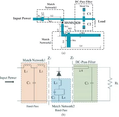
The layout of the proposed rectifier is shown in Figure 2(a). The impedance match network of the rectifier is divided by two parts. The match network 1 is a stepped microstrip line and match network 2 is a cross-shaped stub. The cross-shaped stub as the match network 2 is adopted to generate a dc path and cancel the imaginary part of diode over a broad bandwidth. Furthermore, the cross-shaped stub blocks the second order harmonic generated by the diode. The stepped microstrip line is designed to reduce the reflection coefficient further and improves the mw-dc conversion efficiency. By adjusting the length and width of two-level match network, an additional resonance frequency can be formed. Thus, the rectifier can operate over an extended bandwidth.
The equivalent circuit is shown in Figure 2(b). The open stubs and short stubs are equivalent to capacitance and inductance. The values are given by
jX =jΩL=jLtanθ
jB=jΩC=jCtanθ (1)
Input Power
H
Match Network1
Match Network2
L3
L6
W2 L1
L2
W
L5 W1
HSMS2820 C2
C1 Metal Via
L4 W3
W4 W5
5
W6
DC-Pass Filter
Load
(a)
(b)
Figure 2. (a) Layout and (b) equivalent circuit of the proposed rectifier.
The input impedance of the basic diodeZD is
ZD = πRS
cosθon
θon
cosθon −sinθon
+jωRSCj
π−θon
cosθon + sinθon
(2)
whereθon is the turn-on angle of the diode, and Cj is the junction capacitance of the diode. From the equivalent circuit of the rectifier, the impedance of match network 2 is obtained
Z2 =ZL3+ (ZC2//ZL4) = jω
(L3−ω2C2L3L4+L4)
1−ω2C2L4 (3)
It is observed that the input impedance Z2 has inductor characteristic, which can cancel the imaginary part of ZD. The input impedance of the branch with diode is given as
ZD+Z2= Re(ZD) + Im(ZD +Z2)
When the values ofC2,L3 and L4 are chosen properly, the impedanceZ1 can be obtained
ImZ1(ω1)≈ImZ1(ω2)≈0
The match network 1 has band-pass characteristic, which can adjust the real part ofZ1 and further compensate the imaginary part. The inductanceL2 can cancel the imaginary part ofZ1 and the match network1 can adjust the real part to 50 Ω. A rough equation is given by
ReZ1(ω1)≈ReZ1(ω2)
By designing proper lumped elements, the rectifier can achieve good match characteristic at two resonance frequencies. When two frequency bands are close to each other, a broad impedance bandwidth can be obtained.
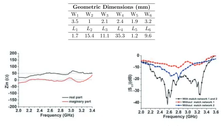
The rectifier is simulated and analyzed by Aglient ADS software. The rectifier is designed on an F4B-2 substrate with the relative dielectric constantεrof 2.65, thicknesshof 0.8 mm and tanβ of 0.001. The capacitance C1 and C2 is designed by 47 pF. The geometric parameters of the rectifier are listed in Table 1. The input impedance Zin of the rectifier versus the frequency is shown in Figure 3. The real and imaginary parts of the input impedance Zin are between 30 ∼ 60 Ω and −10 ∼ 10 Ω when the operation frequency increases from 2.2 GHz to 3.3 GHz. It is observed that the input impedance Zin changes slowly with the frequency in a relatively broad bandwidth, and it is close to the standard impedance of 50 Ω.
Table 1. Dimension of the proposed rectifier.
Geometric Dimensions (mm) W1 W2 W3 W4 W5 W6
3.5 1 2.1 2.4 1.9 3.2
L1 L2 L3 L4 L5 L6
1.7 15.4 11.1 35.3 1.2 9.6
Figure 3. Simulated input impedance Zin vs. frequency.
Figure 4. Simulated |S11|vs. frequency.
The proposed rectifier based on a two-level match network is compared with the rectifiers without the match network 1 or match network 2 in terms of the reflection coefficient, which is displayed in Figure 4. The simulated |S11| of the rectifier without matching network 2 is less than −10 dB when the operation frequency increases from 2.4 GHz to 3.0 GHz. By using the two-level match network, the bandwidth of|S11|less than−10 dB is more than 42.8% (from 2.2 GHz to 3.4 GHz) and the bandwidth of |S11|less than −20 dB is enhanced to 900 MHz (from 2.4 GHz to 3.3 GHz). Moreover, the reflection coefficient has two resonance frequencies. The bandwidth can be extended by generating extra resonance frequency. Thus, the proposed rectifier can extend the operation bandwidth by using two-level match network.
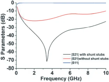
Figure 5. Simulated|S21|and|S11|of the dc-pass filter.
Figure 6. Photograph of the fabricated rectifier.
is designed to suppress the fundamental frequency and high order harmonics. Figure 5 presents the simulated return loss and insertion loss of the dc-pass filter versus the frequency. It can be found that the|S11|is close to 0dB when the frequency increases from 0.1 GHz to 10 GHz. The|S21|is under
−40 dB within the fundamental frequency bandwidth (from 2.2 GHz to 3.2 GHz) and is under−25 dB in the second and third order harmonic bandwidth. The higher order harmonics are too low to contribute to the power loss significantly. Compared with the dc-pass filter without shunt stubs, the proposed dc-pass filter has better performance in harmonic suppression. So the fundamental frequency and high order harmonics can be inhibited effectively by using this proposed dc-pass filter.
3. EXPERIMENTS RESULTS
The fabricated rectifier is shown in Figure 6. The mw-dc conversion efficiency of the rectifier is calculated by the following formula,
η= PDC Pin =
V2
DC/R
Pin (4)
where VDC is the output dc voltage which is measured by a multimeter. PDC is the dc output power on the loadR, and is calculated byVDC and R. Pin is the input power from the CW Generator of HP 83623L. The load is set by adjustable resistance box.
The reflection coefficient|S11| is measured by Agilent 8722ES Vector Network Analyzer, in which the maximum input power is only 15 dBm. The simulated and measured reflection coefficients within different input powers are displayed in Figure 7. It is observed that the measured |S11| agrees with
the simulated result. When the input power is 15 dBm, the rectifier has low reflection coefficient at the resonance frequency, and the bandwidth of |S11| less than −10 dB gradually extends when the input power increases from 5 dBm to 15 dBm. From the simulated results, when the input power is above 15 dBm, the rectifier should obtain lower reflection coefficients. The measured resonance frequency has a difference of 200 MHz with the simulated result. This is probably due to the parasitic effect of the surface mount device component and the manual welding process.
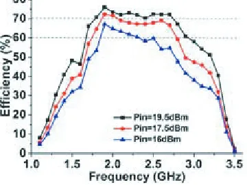
The measured mw-dc conversion efficiencies versus the load, input power and frequency are displayed in Figures 8–10. The load characteristic for the rectifier is investigated at the frequency of 1.9 GHz as shown in Figure 8. It can be found that the measured optimal load is 120 Ω. The mw-dc conversion efficiency with the load resistance of 120 Ω is displayed in Figure 9 when the input power is
Figure 8. Mw-dc efficiency vs. load. Figure 9. Mw-dc efficiency vs. input power.
Figure 10. Mw-dc efficiency vs. frequency.
Table 2. Performance comparison of broadband high-efficiency rectifier.
Ref. Input
Power Bandwidth
Efficiency
over Bandwidth Diode
The Peak Efficiency
[7] 18 dBm 1.6∼2.8 GHz (54.4%) >50% HSMS2862 72.8% [9] 15 dBm 1.65∼3.05 GHz (57%) >50% HSMS2862 78.3% [10] 10 dBm 1.46∼1.76 GHz (18.6%) >70% HSMS2860 81%
[11] 13 dBm 5.2∼6 GHz (14.2%) >70% HSMS2860 75.6%
[12] 17.2 dBm 2.08∼2.58 GHz (21.5%) >70% HMPS2860 80.8% This
from 0 dBm to 22 dBm and frequency is 1.9 GHz. The maximum mw-dc conversion efficiency of 80.3% is gained on the load of 120 Ω when the input power is 22 dBm. The output dc voltage is 3.91 V. Figure 10 shows that the mw-dc efficiency is higher than 70% from 1.8 GHz to 2.72 GHz when the input power is 19.5 dBm and the load is 120 Ω, which also reveals a broadband performance of the rectifier. When the input power is above 19.5 dBm, the bandwidth of efficiencies higher than 70% may be extended further. Thus, the rectifier can achieve high efficiency within a broad operation bandwidth.
Table 2 shows the comparison of bandwidth, efficiency over the operation bandwidth and input power between the proposed rectifier and recent publications. The proposed rectifier owns mw-dc efficiency higher than 80% and a wider bandwidth of efficiency higher than 70%. Compared with the other broadband rectifier, the proposed rectifier has obvious advantages in the mw-dc efficiency and bandwidth.
4. CONCLUSIONS
In this paper, a broadband high-efficiency rectifier based on a two-level impedance match network has been presented. The two-level impedance match network is designed to extend the operation bandwidth. A broadband dc-pass filter is designed to block harmonic power over a broad bandwidth. The measured results have shown that the proposed rectifier has a maximum conversion efficiency of 80.3% on the load of 120 Ω when the input power is 22 dBm, and the bandwidth of efficiencies higher than 70% is about 40% (from 1.80 GHz to 2.72 GHz). Furthermore, the rectifier possesses the characteristics of a simple structure and easy integration, which can be applied in the WSN and RFID systems.
REFERENCES
1. Jiang, S. and S. V. Georgakopoulos, “Optimum wireless powering of sensors embedded in concrete,”
IEEE Transactions on Antennas & Propagation, Vol. 60, No. 2, 1106–1113, 2012.
2. Cheng, H. W., T. C. Yu, and C. H. Luo, “Direct current driving impedance matching method for rectenna using medical implant communication service band for wireless battery charging,”Iet Microwaves Antennas &Propagation, Vol. 7, No. 4, 277–282, 2013.
3. Ge, J. J. and L. Jin, “A modified rectenna for Ka band wireless power transmission,”International Symposium on Computational Intelligence and Design, 185–188, 2015.
4. Lu, J. J., X. X. Yang, H. Mei, et al., “A four-band rectifier with adaptive power for electromagnetic energy harvesting,” IEEE Microwave & Wireless Components Letters, Vol. 26, No. 10, 819–821, 2016.
5. Sun, H. and G. Wen, “A new rectenna with all-polarization-receiving capability for wireless power transmission,” IEEE Antennas& Wireless Propagation Letters, Vol. 15, 814–817, 2016.
6. Huang, W., B. Zhang, X. Chen, K.-M. Huang, and C.-J. Liu, “Study on an S-band rectenna array for wireless microwave power transmission,”Progress In Electromagnetics Research, Vol. 135, 747–758, 2013.
7. Nie, M. J., X. X. Yang, G. N. Tan, et al., “A compact 2.45 GHz broadband rectenna using grounded coplanar waveguide,” IEEE Antennas &Wireless Propagation Letters, Vol. 14, 986–989, 2015. 8. Wang, D., M. D. Wei, and R. Negra, “Design of a broadband microwave rectifier from 40 MHz to
4740 MHz using high impedance inductor,”Microwave Conference, 1010–1012, 2015.
9. Nie, M. J., X. X. Yang, et al., “A broadband rectifying circuit with high efficiency for microwave power transmission,”Progress In Electromagnetics Research Letters, Vol. 52, 135–139, 2015. 10. Sakaki, H. and K. Nishikawa, “Broadband rectifier design based on quality factor of input matching
circuit,” Microwave Conference, 1205–1207, 2015.
11. Wu, P., L. Zhang, C. Liu, et al., “A C-band microwave rectifier based on harmonic termination and with input filter removed,” Wireless Power Transfer Conference, 2017.