University of Windsor University of Windsor
Scholarship at UWindsor
Scholarship at UWindsor
Electronic Theses and Dissertations Theses, Dissertations, and Major Papers
2016
Electronic Properties of Nanoscale Structures/Devices Atomically
Electronic Properties of Nanoscale Structures/Devices Atomically
Engineered on Metal Surfaces
Engineered on Metal Surfaces
Brendan Rhyno
University of Windsor
Follow this and additional works at: https://scholar.uwindsor.ca/etd
Recommended Citation Recommended Citation
Rhyno, Brendan, "Electronic Properties of Nanoscale Structures/Devices Atomically Engineered on Metal Surfaces" (2016). Electronic Theses and Dissertations. 5864.
https://scholar.uwindsor.ca/etd/5864
This online database contains the full-text of PhD dissertations and Masters’ theses of University of Windsor students from 1954 forward. These documents are made available for personal study and research purposes only, in accordance with the Canadian Copyright Act and the Creative Commons license—CC BY-NC-ND (Attribution, Non-Commercial, No Derivative Works). Under this license, works must always be attributed to the copyright holder (original author), cannot be used for any commercial purposes, and may not be altered. Any other use would require the permission of the copyright holder. Students may inquire about withdrawing their dissertation and/or thesis from this database. For additional inquiries, please contact the repository administrator via email
Electronic Properties of Nanoscale
Structures/Devices Atomically
Engineered on Metal Surfaces
By
Brendan Rhyno
A Thesis
Submitted to the Faculty of Graduate Studies through the Department of Physics
in Partial Fulfillment of the Requirements for the Degree of Master of Science
at the University of Windsor
Windsor, Ontario, Canada
2016
c
Electronic Properties of Nanoscale Structures/Devices
Atomically Engineered on Metal Surfaces
by
Brendan Rhyno
APPROVED BY:
J. Rawson
Department of Chemistry & Biochemistry
C. Rangan
Department of Physics
E. H. Kim, Advisor
Department of Physics
Declaration of Originality
I hereby certify that I am the sole author of this thesis and that no part of this thesis has
been published or submitted for publication.
I certify that, to the best of my knowledge, my thesis does not infringe upon anyone’s
copyright nor violate any proprietary rights and that any ideas, techniques, quotations, or any other material from the work of other people included in my thesis, published or
otherwise, are fully acknowledged in accordance with the standard referencing practices. Furthermore, to the extent that I have included copyrighted material that surpasses the
bounds of fair dealing within the meaning of the Canada Copyright Act, I certify that I have obtained a written permission from the copyright owner(s) to include such material(s)
in my thesis and have included copies of such copyright clearances to my appendix.
I declare that this is a true copy of my thesis, including any final revisions, as approved
by my thesis committee and the Graduate Studies office, and that this thesis has not been submitted for a higher degree to any other University or Institution.
Abstract
Currently, there is interest in using a bottom-up approach to fabricate nanostructures i.e.
structures whose dimensions are on the order of 10−9 metres. Discovering devices which exploit/thrive on quantum mechanical effects is vital if the down-sizing of electronics is
to continue. The aim of this Thesis is to theoretically design and characterize nanoscale structures/devices built atom-by-atom in a bottom-up approach on a metal surface. By
varying the properties of our “building blocks” (i.e. atoms), we demonstrate that one can engineer devices which purposefully exploit novel physics. More specifically, we demonstrate
how the strongly correlated state induced by magnetic atoms in a metal can be used for control and transmission of signals between distinct points. Furthermore, we demonstrate a
mechanism to drive superconductivity in a single atom; we utilize this mechanism to create superconducting nanostructures with precisely designed properties.
Acknowledgements
First and foremost, I must thank Dr. Eugene Kim for the countless hours spent discussing
physics, research, and life – I am truly grateful to have had the opportunity to work/learn in such an environment. Without our interactions, I can honestly say I would not be the
same physicist (or person) that I am today. Thank you.
To my best friend and partner in life, my wife Shelby Rhyno: thank you for always being
by my side and supporting me (even when I am a goof). I cannot wait to start the next chapter of our lives together!
This list would not be complete if I did not thank my parents for their constant support and for encouraging me to study science.
Finally, I am grateful to the Government of Ontario, Natural Sciences and Engineering Research Council of Canada (NSERC), and University of Windsor for providing me with
financial support throughout the duration of this work.
Table of Contents
Declaration of Originality iii
Abstract iv
Acknowledgements v
List of Figures viii
1 Introduction 1
1.1 Present-Day Electronics; Top-Down vs. Bottom-Up . . . 1
1.2 Atomic-Scale Engineering . . . 3
1.3 The System . . . 5
1.3.1 The Surface . . . 5
1.3.2 Impurity Atoms . . . 6
1.3.3 The Bulk . . . 7
1.4 Thesis Contributions and Outline . . . 8
1.5 Notes . . . 9
2 Scattering Formalism 10 2.1 Green’s Functions and the Dyson Equation . . . 10
2.1.1 A Single Scatterer . . . 12
2.1.2 Multiple Scatterers . . . 13
2.2 Quantum Corrals . . . 15
3 Signal Control and Transmission Using Magnetic Atoms 16 3.1 The Kondo Problem . . . 16
3.1.1 Background . . . 16
3.1.2 The Infrared Fixed Point . . . 18
3.2 The Kondo Mirage . . . 21
3.3 Signal Control and Transmission . . . 24
4 Atomic-Scale Engineering of Superconducting Nanostructures 28 4.1 Superconductivity . . . 29
4.1.1 Background . . . 29
4.1.2 Superconducting Atoms . . . 32
4.2 Scattering Formalism: Superconducting Impurities . . . 33
4.3 Engineering Superconducting Nanostructures . . . 36
5 Conclusion 40
Table of Contents vii
Appendices 42
A Momentum Sums . . . 43
A.1 Two Dimensions . . . 43
A.2 Three Dimensions . . . 44
A.3 Examples . . . 44
B Second Quantization . . . 46
B.1 Identical particles . . . 46
B.2 Second Quantization . . . 47
B.3 Thermal Expectation Values of Fermion Bilinears . . . 50
B.4 Green’s Functions . . . 51
B.5 The Spectral Representation . . . 52
C Theory of Superconductivity . . . 53
C.1 Mean-Field Superconducting Hamiltonian . . . 53
C.2 The Gap Equation . . . 55
C.3 Superconducting Density of States . . . 57
C.4 Green’s Function for a Superconductor . . . 58
D Green’s Function for a Two-Dimensional Electron Gas . . . 61
E Effective Scattering Potentials . . . 65
E.1 Black-dot Approximation . . . 66
F Spin Operators . . . 67
F.1 Spin Density Operator . . . 67
F.2 Spin-Spin Coupling . . . 68
G Green’s Functions with Magnetic Impurities . . . 69
G.1 Green’s Functions for the Magnetic Atom . . . 69
G.1.1 Mean-Field Equations . . . 71
G.2 Green’s Function for the Conduction Electrons . . . 72
G.3 Green’s Function for Two Magnetic Atoms in a Metal . . . 73
Bibliography 76
List of Figures
1.1 The Transistor . . . 2
1.2 Tunneling through a Barrier . . . 2
1.3 The Scanning Tunneling Microscope . . . 4
1.4 Face-Centered Cubic Lattice and the (111) Plane . . . 6
1.5 Single Adatom on a Metal Surface . . . 7
1.6 Multiple Adatoms on a Metal Surface – Engineering Electronic Wave Functions 7 2.1 Density of States of a Quantum Corral . . . 15
3.1 Resistivity Minimum of Dilute Magnetic Alloys . . . 17
3.2 The Kondo Resonance . . . 18
3.3 A Magnetic Impurity in a Quantum Corral . . . 21
3.4 The Kondo Mirage . . . 22
3.5 The Mirage Signal . . . 23
3.6 Magnetic Atom Signal Modulation Device . . . 24
3.7 Two Magnetic Impurities in a Quantum Corral . . . 25
3.8 Results: Signal Control and Transmission Using Magnetic Atoms . . . 27
4.1 Defining Properties of Superconductors . . . 29
4.2 Interacting with the Lattice: An Attractive Interaction Between Electrons . 30 4.3 The Cooper Problem . . . 31
4.4 A Cooper Pair . . . 31
4.5 A Superconducting Atom . . . 33
4.6 Atomically Engineered Superconducting Nanostructure . . . 37
4.7 Results: Superconducting Quantum Corral – the Josephson Current . . . . 38
4.8 Results: Atomically Engineered Andreev Bound States . . . 39
C.1 Superconducting Density of States . . . 58
D.1 Arguments for the Green’s Function . . . 63
Chapter 1
Introduction
1.1
Present-Day Electronics; Top-Down vs. Bottom-Up
Semiconductor devices lie at the heart of present-day electronics. The central element used to process information is the transistor. Invented in 1947 by Bardeen, Brattain, and
Shockley, the transistor has revolutionized technology, earning its creators the Nobel Prize in Physics “for their researches on semiconductors and their discovery of the transistor
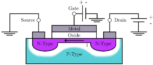
effect” in 1956.[1] Fig. 1.1 shows a schematic of the metal-oxide-semiconductor field-effect transistor. The bulk of the device consists of a doped silicon crystal – while Si is an
intrinsic semiconductor, doping (with impurity atoms) changes its electrical properties;[2] hence, making it possible tocontrol the current through the device via electric fields. It is
important to appreciate how information is transferred between locations in a transistor – information is physically carried from one point to another by the flow of currents between
the source and drain electrodes.
For many years, engineers have successfully found ways to shrink transistor devices and
hence, increased the capacity for complex computation. In fact, Gordon Moore (co-founder of Intel) noticed that approximately every 1 to 2 years the number of transistors which could
be fitted onto a single integrated circuit doubled.[3] This observation has held true for the past few decades and is now deemed “Moore’s Law”; as a result of this downsizing, current
transistors are nanostructures with dimensions on the order of 10’s of nanometres.[4]
Chapter 1. Introduction 2
Figure 1.1: Schematic of the transistor. The “P-Type” (“N-Type”) regions are doped
with acceptor (donor) atoms resulting in holes (electrons) being the majority charge carrier.[2] Along each region’s boundary, electrons and holes recombine forming a depletion region. Two metal electrodes are placed on the N-type regions called the source and drain; another electrode called the gate is placed on top of an insulating oxide layer. If the drain and source are held at a (low) potential difference, one can send a current between the two by applying a voltage across the gate.
Moore’s law epitomizes the technological revolution we currently enjoy, but it is also a
warning of things to come – as current devices/technology shrink down further, quantum effects must be taken into account.[5] For transistors, quantum tunneling poses the most
severe problem. Tunneling is a purely quantum phenomenon exhibited by particles when faced with an energy barrier – classically, a particle cannot overcome an energy barrier
unless provided with sufficient additional energy; however, quantum mechanics gives a finite probability that the particle will be found on the opposite side of the barrier (Fig. 1.2).
Fundamentally, transistors work on the assumption that we control the flow of current through them; hence, with the present design, tunneling gives an uncontrollable contribution
to the current.
Chapter 1. Introduction 3
Further problems arise when one considers the pathways in which information travels be-tween devices: theinterconnect wires.[6] Modern chips require a dense array of interconnect
wires to relay information (i.e. currents) from one transistor to another.[6, 7] Interconnect wires built from conducting materials such as copper and aluminum suffer from scaling,
because their resistivity increases as their dimensions decrease into the nanoscale.[6, 8, 9] This coupled with the increased current density each wire must support when downsized
leads to concerns over the Joule heating of the wires.[10]
Therefore, further advancements in electronics and, more generally, information processing
will require the development of new technologies that embrace quantum effects. To realize these technologies, new systems/approaches are needed. Integrated circuits are currently
fabricated using top-down methods[7] – semiconducting crystal wafers are put through a series of material deposit and photolithographic steps to produce a finished circuit which
contains (billions of) devices connected via metallic pathways.[4, 7] However, nanometre-scale devices enable an opposite means of fabrication, namelybottom-up– a desired structure
is built-up piece by piece using smaller “building blocks” of matter. Inherently, a top-down process is subtractive whereas a bottom-up process is additive.[11]
With this in mind, the goal of this Thesis is to consider a class of nanostructures built bottom-up. Specifically, we design and characterize the properties of structures/devices
built atom-by-atom on metal surfaces. By controlling matter on the smallest of scales, these systems allow us to investigate novel physics with the prospect of potential device
applications.
1.2
Atomic-Scale Engineering
The tool employed both to probe and build these structures is the scanning tunneling microscope (STM).[12] Designed in 1981 by Binnig and Rohrer at IBM, the STM utilizes the
phenomenon of quantum tunneling to image matter on the nanoscale.[13] The significance of this device was immediately appreciated and its inventors were awarded the Nobel prize
Chapter 1. Introduction 4
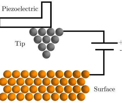
Pictured in Fig. 1.3 is a schematic of the device: the STM consists of an atomically sharp tip brought near a surface (their separation on the order of ˚A’s); as a result, electrons
tunnel between the tip and surface generating a tunneling current.[15, 16] A small bias voltage (less than 0.3[V])[12] is applied between the tip and surface to precisely control this current. Piezoelectric materials (materials which expand or contract in the presence of an electric field) are then used to control the motion of the tip in space.[15, 16]
Figure 1.3: Schematic of the scanning tunneling microscope. A piezoelectric material translates an atomically sharp tip through space. When the tip is biased with respect to the surface, electrons tunnel to the surface resulting in a current.
The two most common measurements made with an STM are the so-called spectroscopic
and topographic measurements. In a spectroscopic measurement, the tunneling current (or differential conductancedI/dV) is measured as the bias voltage between the tip and surface is swept (while holding the tip’s spatial position fixed).[16] In a topographic measurement, the tip’s height is measured as its position in the plane of the surface is swept (while holding
the bias voltage and tunneling current fixed). A constant current is achieved by providing a feedback loop to the piezoelectric servo aligned in the axis of the tip.[16] Furthermore,
experiments have been carried out where topographic and differential conductance maps of the surface are generated simultaneously.[17, 18]
The differential conductance measured in STM experiments is proportional to the local density of states (LDOS) for electrons on the surface:
A(r;ω) =X n
Chapter 1. Introduction 5
where {φn(r)} ({εn}) are the wave functions (eigenvalues) for the surface electrons.[12, 19] [The tunneling current is then proportional to an integral of the LDOS over energy.]
Therefore, the physical quantity of primary interest is the LDOS. One finds that the LDOS can be computed efficiently via A(r;ω) = −(1/π)Im[G(r,r;ω)] where G(r,r0;ω) is the (retarded) Green’s function for the surface electrons.[12, 19]
In 1990, Eigler and Schweizer demonstrated that an STM could also be used to perform atomic-scale engineering; specifically, to position individual impurity atoms (or adatoms)
embedded in a host material.[20] They achieved this by bringing an STM tip towards an impurity and applying a sufficiently high voltage such that the atom’s bond with the
substrate was overcome. The impurity was then relocated to a region of interest.[20, 21] This atomic-scale control is exciting because it allows one to build structures not found in nature.[17, 18, 22]
1.3
The System
To proceed, it is essential to discuss the substrate on which these structures are engineered; namely, the surface of noble metals. It is also essential to discuss the bulk material below
as this plays a subtle but essential role in determining the system’s electronic properties.
1.3.1 The Surface
These structures are typically fabricated on the surface of a noble metal (such as copper, silver, and gold).[17, 22] In their crystalline form, these elements form a face-centered cubic
(fcc) lattice (Fig.1.4).[23] The (111) plane of this lattice is of particular interest, as the surface states resulting from this cut are orthogonal to the material’s bulk states – the wave
function of a surface state decays exponentially fast into the bulk and vacuum.[12] This is important/useful, as the electrons on the surface essentially move within the plane of the
surface – the surface states areisolated from the bulk states.
More precisely, electrons on the (111) surface constitute a two-dimensional electron gas
Chapter 1. Introduction 6
Figure 1.4: Left – the unit cell of a face-centered cubic lattice. By cutting the lattice
along the direction shown with the (blue) coloured surface, one obtains the (111) plane. Right – the arrangement of the atoms in the (111) plane.
momentum,m is its effective mass, andEF is the Fermi energy of the surface state. [Note: As written, εp measures the energy with respect to the Fermi energy.] Being able to treat
the surface as a 2DEG is advantageous, because having an isotropic dispersion (i.e. the
same in all directions of momentum space) enables one to carry out calculations without considering the orientation of the lattice.[12] In this Thesis, we focus on the Cu(111) surface
as it is most relevant to experiment.[17, 22] Electrons in the 2DEG of the Cu(111) surface have an effective mass ofm = 0.38me (me is the bare electron mass) with a Fermi energy of EF = 450[meV].[17, 18]
1.3.2 Impurity Atoms
Introducing impurity atoms has stunning consequences – STM experiments reveal that wave patterns form around the sites of the impurities (Fig.1.5).[22] These waves are a result of
electrons in the 2DEG scattering off of the impurity atoms. In treating these scattering centers theoretically, it is useful to know that the Fermi wavelength for a Cu(111) surface is
λF = 2.95[nm][12, 19] – the wavelength of the electrons in the 2DEG is far larger than the size of the impurity atoms themselves. Since we will be interested in the system’s low-energy
(orinfrared) properties, one can disregard higher orbital channels and treat the impurities simply as s-wave scatterers;[12, 19] namely, we treat the impurity atoms as delta function
scatterers.
Chapter 1. Introduction 7
Figure 1.5: Electron probability density from a single adatom on a metal surface. The
scattered electrons give rise to a wave pattern emanating from the atom.
describes a standing wave (e.g. a “particle in a box”).[24, 25] In the 1990s researchers began to exploit this by using STMs to form (nearly) closed geometries with impurity atoms on
a metal surface – the structures were deemed quantum corrals (QCs).[12] The electron scattering results, as revealed by STM measurements, are stunning for their intrinsic beauty
but also because they provide a window from which to view the system’s wave function itself (recall Eq. 1.1).
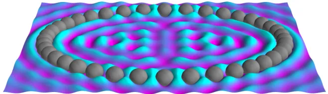
Figure 1.6: Electron probability density from multiple adatoms on a metal surface. When arranged in a closed structure – a quantum corral – the interference between the surface electron waves from scattering off the adatoms leads to a nontrivial structure inside the corral.
As an example, consider the LDOS of an elliptical QC shown in Fig. 1.6. The unique
wave pattern which forms from the superposition of the surface electrons’ wave functions is clearly visible in the image. Furthermore, this elliptical structure is of particular interest
to us as it will be the platform for the structures/devices we will consider in subsequent Chapters.
1.3.3 The Bulk
Chapter 1. Introduction 8
atom, surface electrons are absorbed into the bulk and bulk electrons tunnel to the surface – i.e. at impurity locations, surface states and bulk states are no longer orthogonal.[12] It is
through this coupling that the bulk makes its presence “felt” on the surface. Therefore, the effect of placing an impurity atom on the surface at positionr0 is described by the potential
ˆ
V =UX
s
ψs†(r0)ψs(r0) +C X
s h
ψ†s(r0)χs(r0) +χ†s(r0)ψs(r0) i
(1.2)
whereU is the strength of scattering on the surface (in the s-wave channel),Cis the strength of the coupling between the surface and the bulk, and ψs(r) (χs(r)) are electron field operators for the surface (bulk) at position rwith spin-s. [Appendix B gives a description of second quantization (as needed for this Thesis).]
It has been shown that one achieves good quantitative agreement with experiment when
impurities are treated using theblack-dot approximation.[12] Namely, the coupling between the surface and bulk (due to the presence of the impurity atom) is so strong that other
scattering processes can be ignored: U → 0. Historically, the absorption of electrons into the bulk has been seen as a hindrance;[12] however, it is precisely this effect that we exploit
later when we investigate bulk materials with properties different from the surface layer.
1.4
Thesis Contributions and Outline
The rest of this Thesis is organized as follows:
In Chapter 2, we discuss the formalism to calculate/characterize the electronic properties
of these systems; namely, we develop the scattering formalism.
In Chapter 3, we present a novel means of controlling and transmitting signals utilizing
magnetic atoms. We begin by reviewing the key physics exhibited by magnetic atoms embedded in metals; namely, the Kondo effect. We then review the seminal experiments
which demonstrated how this effect can be used to transmit a signal between distinct points in a QC. We review/develop the appropriate formalism to describe the physics. To conclude,
Chapter 1. Introduction 9
In Chapter 4, we present a novel means of fabricating superconducting nanostructures on the smallest scale; namely, atom-by-atom. We begin by reviewing the central properties
of superconductors. We then discuss a novel mechanism to make individual atoms exhibit superconducting properties and extend the scattering formalism to allow for these atoms.
Lastly, we describe our work demonstrating atomic-scale engineering of superconducting nanostructures and, in particular, precise control over the electronic properties of these
structures.
Chapter 5 contains a summary and prospects for future work.
Finally, a collection of Appendices that contain details of the calculations is included.
1.5
Notes
All the calculations in this Thesis are carried out in units where ~= 1.
For normalization purposes, we put our systems in a large box of volume V[= Ld, where
Chapter 2
Scattering Formalism
The intention of this Thesis is to discuss the engineering of nanoscale systems/devices using
adatoms on metal surfaces. In this Chapter, we develop a formalism to understand and, more practically, compute the (electronic) properties of these systems; namely, here we
outline the scattering formalism.
2.1
Green’s Functions and the Dyson Equation
Consider a system of fermions with second quantized Hamiltonian ˆH =P n
Enc†ncn, where
cn annihilates a fermion of energyEn (Appendix B). Define theGreen’s function as
G(r,r0;t) :=−iΘ(t)h{ψ(r;t), ψ†(r0)}i (2.1) whereψ(r;t) is the system’s field operator at positionrand timet,h· · ·idenotes a thermal average,{· · · }is the anticommutator, and Θ(t) is the Heaviside step function. The physical quantity of interest is the local density of states (LDOS)A(r;ω), as this is what is measured in STM experiments;[12] explicitly,
A(r;ω) =−1
πIm[G(r,r;ω)] (2.2)
Chapter 2. Scattering Formalism 11
where G(r,r0;ω)=R dt eiωtG(r,r0;t) is the Fourier transform of Eq. 2.1. Expanding the field operators in terms of the{cn} gives
G(r,r0;ω) =X n
φn(r)φ∗n(r0)
ω−En+iδ
(2.3)
where {φn(r)} are the single-body wave functions of the Hamiltonian and δ(= 0+) is a convergence factor. Notice that one must know the energy eigenvalues and eigenfunctions to compute the Green’s function with Eq. 2.3.
Starting with Eq. 2.1 is not always the most convenient way to proceed. Alternatively, one can make use of the resolvent operator:
ˆ
G= (ω−Hˆ +iδ)−1 (2.4) where ˆH is the Hamiltonian, and ω is a real scalar. [As before, δ = 0+.] In particular, by using the corresponding single-body operator for the second quantized Hamiltonian (also
denoted by ˆH) and projecting ˆGonto position representation one obtains
G(r,r0;ω) =hr|(ω−Hˆ +iδ)−1|r0i . (2.5) One can show that this is an equivalent form of the Green’s function by expanding in the eigenkets of the single-body Hamiltonian,{|ni}, and letting the operator act on the energy kets. Doing this yields Eq. 2.3 whereφn(r) =hr|ni.
Our primary focus is systems containing impurity atoms; the Hamiltonian of such a system
can be written as
ˆ
H= ˆH0+ ˆV (2.6)
where ˆH0 is the Hamiltonian of the bare system (i.e. the Hamiltonian without impurities) and ˆV is ascattering potential arising from the impurity atoms. By making the definition
ˆ
G0 := (ω−Hˆ0+iδ)−1 and using that ( ˆABˆ)−1= ˆB−1Aˆ−1 one obtains the Dyson equation: ˆ
Chapter 2. Scattering Formalism 12
To obtain the Green’s function from the Dyson equation, consider the corresponding single-body operators for the system and project onto position representation:
G(r,r0;ω) =G0(r,r0;ω) + Z
dr1dr2G0(r,r1;ω)hr1|Vˆ |r2iG(r2,r0;ω) (2.8) where the bare Green’s function has been defined as G0(r,r0;ω) := hr|Gˆ0|r0i. We see that the Dyson equation enables one to determine the system’s (full) Green’s function from the
bare Green’s function.
2.1.1 A Single Scatterer
We now apply this formalism to some example systems which are relevant to the rest of
the Thesis. First, consider a two-dimensional electron gas (2DEG) with a single scattering center (an impurity atom) located at position r0. The Hamiltonian used to describe the
system is ˆH = ˆH0+ ˆV, where ˆH0 is the Hamiltonian of the 2DEG and ˆV is the scattering potential due to the impurity. To simplify things, we take the scattering potential to be an
s-wave scatterer i.e. a delta function.[12] Approximating the impurity as a point scatterer is justified because the wavelength of electrons on the surfaces of interest (noble metals such
as copper and gold) are far larger than the size of the impurity itself.[12]
Our goal is to obtain the system’s Green’s function. To that end, consider the Hamiltonian’s
corresponding single-body operator: Hˆ = ˆH0 + ˆV where ˆH0[= (1/2m)ˆp2 −EF] is the Hamiltonian of a free-particle and ˆV[= V0δ(ˆr−r0)] is the potential due to the impurity withV0 characterizing the scattering phase shift (see Appendix E). [Note: We are measuring energies with respect to the Fermi energy EF.] By inserting the scattering potential into Eq. 2.8 one obtains
Chapter 2. Scattering Formalism 13
Eq. 2.9 to obtain
G(r,r0;ω) =G0(r,r0;ω) +G0(r,r0;ω)T(ω)G0(r0,r0;ω) (2.10) where theT-matrix has been defined as
T(ω) := V0
1−G0(r0,r0;ω)V0
. (2.11)
2.1.2 Multiple Scatterers
Next, consider a collection of (s-wave) impurity atoms in a 2DEG. Similar to the case of a single scatterer, the Hamiltonian of this system is described by ˆH = ˆH0+ ˆV where ˆH0 is the Hamiltonian of the 2DEG and ˆV is the scattering potential arising from the presence of the multiple impurities.
Again, we will use the Dyson equation to compute the Green’s function. Consider the corresponding single-body Hamiltonian: ˆH= ˆH0+ ˆV where ˆH0is the Hamiltonian of a free-particle and the scattering potential is given by ˆV =V0P
i
δ(ˆr−ri) with{ri} representing the locations of the impurities. Proceeding in the same fashion as before, we insert this
potential into the Dyson equation. Integrating over the resulting delta functions yields
G(r,r0;ω) =G0(r,r0;ω) +X i
G0(r,ri;ω)V0G(ri,r0;ω). (2.12) Introduce the following vectors:
G(r;ω) :=
G(r1,r;ω)
G(r2,r;ω) .. .
, G0(r;ω) :=
G0(r1,r;ω)
G0(r2,r;ω) .. . . (2.13)
Writing the Dyson equation in terms of these vectors gives
G(r,r0;ω) =G0(r,r0;ω) +G T
Chapter 2. Scattering Formalism 14
expression for the Green’s function, analyze the Dyson equation at r = ri. Carrying out this procedure for every impurity site and organizing the results as a matrix yields
G(r0;ω) =G0(r0;ω) + ˆG0(ω)V0G(r0;ω) (2.15) where the matrix ˆG0(ω) has been defined as
ˆ
G0(ω) :=
G0(r1,r1;ω) G0(r1,r2;ω) . . .
G0(r2,r1;ω) G0(r2,r2;ω) . . . .. . ... . .. . (2.16)
One can obtain a solution for the vector of Green’s functions by solving Eq. 2.15:
G(r0;ω) =hI−Gˆ0(ω)V0 i−1
G0(r0;ω) (2.17) Inserting the solution back into the Dyson equation gives an explicit expression for the
Green’s function. Namely,
G(r,r0;ω) =G0(r,r0;ω) +G T
0(r;ω) ˆT(ω)G0(r0;ω) =G0(r,r0;ω) +
X
i,j
G0(r,ri;ω) ˆTi,j(ω)G0(rj,r0;ω) (2.18) where the T-matrix has been defined as
ˆ
T(ω) :=V0 h
I−Gˆ0(ω)V0 i−1
. (2.19)
From Eq. 2.10 (a single scatterer) and Eq. 2.18 (multiple scatterers) it is clear that the
Green’s function is constructed using the free-particle Green’s function. Computing the free-particle Green’s function in two-dimensions (or the Green’s function of a 2DEG) yields
(Appendix D)
G0(r,r0;ω) = (
−i(πρ0)H0(1)(k|r−r0|) ,r6=r0
−i(πρ0) +ρ0ln
EF+ω
D−ω
,r=r0
(2.20)
Chapter 2. Scattering Formalism 15
and H0(1)(x) is a Hankel function.[26]
2.2
Quantum Corrals
The formalism discussed so far is suitable to describe the results of quantum corral (QC) experiments.[12] Similar to what has been realized experimentally, we consider the case
of 40 impurity atoms arranged in an ellipse, (x/a)2 + (y/b)2 = 1, where a/b = 1.5 with
a= 8.583[nm] on a Cu(111) surface – EF = 0.45[eV] andm= 0.38me.[17, 18]
We apply Eq. 2.18 to obtain the Green’s function of the QC. To do this, as discussed in Chapter 1, we treat the s-wave scattering phase shift in the black-dot approximation.[12]
By computing the LDOS from the Green’s function via Eq. 2.2, we obtain the spatial map in Fig. 2.1. In agreement with experiment, our calculations produce distinct standing wave
patterns inside the walls of the corral.[17, 27]
Chapter 3
Signal Control and Transmission
Using Magnetic Atoms
Seminal experiments have shown how a magnetic impurity can be used to transmit a signal between distinct points in a quantum corral: the Kondo mirage.[17] In this Thesis, we are
interested in the prospect of controlling the transmitted signal.
In this Chapter, we review key properties/results of the Kondo problem; we then discuss
a formalism to treat the Kondo model and, in particular, its infrared properties. We also review key properties of the mirage experiment. Finally, we discuss how two magnetic
impurities in a quantum corral can be used to control transmitted signals.
3.1
The Kondo Problem
3.1.1 Background
The Kondo problem deals with a single magnetic impurity in a metal host. Investigations
of this problem began by trying to understand the resistivity minimum displayed by dilute magnetic alloys[28] – as the temperature is lowered, one finds a metal’s resistivity decreases
because electron-phonon scattering becomes less of a burden;[28–30] however, in the 1930s experiments revealed that doping a metal with magnetic impurities introduces a minimum
Chapter 3. Signal Control and Transmission Using Magnetic Atoms 17
in the resistivity as a function of temperature (Fig. 3.1).[28]
Figure 3.1: The resistivity of a dilute magnetic alloy, R vs. T. As T is lowered, R
decreases; after passing a critical value,R rises again. Shown with a dotted black line is the resistivity of a metal without magnetic impurities; in this case,R vs.T is monotonic.
The first satisfactory explanation of the resistivity minimum was given by Jun Kondo in 1964.[31] Kondo considered the Hamiltonian
ˆ
H= ˆH0+ ˆV (3.1)
where ˆH0 is the Hamiltonian of the metal and ˆV is the potential that arises from the coupling of the spin degree of freedom of the magnetic atom (MA) to those of the metal.
Explicitly,
ˆ
H0= X
p,s
εpc†p,scp,s (3.2) where cp,s destroys an electron of momentum p and spin-s in the metal and the single-particle dispersion is εp =p2/2m−EF. The potential was taken as
ˆ
V =Jτ¯·S(r0) (3.3)
where J is a (positive) coupling constant, ¯τ is the MA’s spin operator, and S(r0) is the spin density operator of the metal (evaluated at the location of the MA): S(r) =
(1/2)P s,s0
ψ†s(r)¯σs,s0ψs0(r) where ψs(r) is the electron field operator of the metal at position
rwith spin-sand {σµ}are Pauli matrices in spin space (Appendix F). Using perturbation theory, Kondo computed the resistivityR(T) and obtained
Chapter 3. Signal Control and Transmission Using Magnetic Atoms 18
where the first term is due to scattering from inert impurities, the second term is the phonon contribution, and the final term is due to scattering from the MAs. [In Eq. 3.4, D is the bandwidth of the conduction electrons anda andb are (positive) constants.]
While Kondo’s calculation was able to explain the resistivity minimum (through the log-arithmic term arising from the scattering off of magnetic impurities), it also signaled that
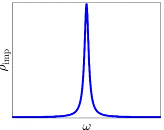
this (seemingly) simple Hamiltonian (Eq. 3.1) has highly nontrivial physics buried in it – the logarithm diverges as T → 0; therefore, perturbation theory breaks down and the ground state is a strongly correlated state. After much struggle, it came to be understood this strongly correlated state consists of a cloud of conduction electrons locked in a singlet with the impurity.[28] The state manifests itself via a resonance in the density of states at
(or near) the Fermi energy, known as the Kondo resonance (KR).
Figure 3.2: The density of states of a magnetic impurity in a metal host, ρimp vs. ω.
Due to the interaction between conduction electrons and the magnetic atom, one observes a resonance in the impurity density of states at the Fermi energy.
3.1.2 The Infrared Fixed Point
We will be interested in utilizing the strongly correlated ground state of the Kondo Hamil-tonian for signal transmission; hence, we need to develop an approach appropriate for
low-energies. To this end, we employ a fermionic representation for the MA’s spin operator[28]
¯
τ = 1 2
X
s,s0
fs†σ¯s,s0fs0 (3.5)
Chapter 3. Signal Control and Transmission Using Magnetic Atoms 19
the spin’s physical Hilbert space; namely, there is always a single (spin-up or spin-down) fermion on the impurity site. We achieve this by imposing the constraint
X
s
fs†fs = 1 . (3.6)
Using Eq. 3.5, one can show the spin-spin coupling can be written as (Appendix F)
¯
τ ·S(r0) =−1
2 X
s,s0
[ψs†(r0)fs][fs†0ψs0(r0)] + const. (3.7)
By inserting Eq. 3.7 into the Hamiltonian one obtains
ˆ
H=X
p,s
εpc†p,scp,s−
J
2 X
s,s0
[ψ†s(r0)fs][fs†0ψs0(r0)] (3.8)
where the unimportant constant value has been removed for convenience (i.e. we have shifted our energy scale); then, to enforce the constraint on the Hilbert space (Eq. 3.6), we
employ a Lagrange multiplier, λ– we arrive at the effective Hamiltonian
ˆ
Heff= X
p,s
εpc†p,scp,s−
J
2 X
s,s0
[ψs†(r0)fs][fs†0ψs0(r0)] +λ
X
s
fs†fs−1 !
. (3.9)
To proceed, we use that our interests are solely in the infrared properties of the system.
Guided by the physics, we analyze Eq. 3.9 using mean-field theory. Specifically, using that theinfrared fixed point of the Kondo model is such that a cloud of conduction electrons is
locked in a singlet with the impurity spin, we approximate
[ψs†(r0)fs][fs†0ψs0(r0)]→ hψs†(r0)fsif†
s0ψs0(r0) +ψ†s(r0)fshf†
s0ψs0(r0)i . (3.10)
Furthermore, we treat the constraint on average – we demand that ∂λhHˆi= 0 whereh· · ·i represents a thermal average. Doing so yields
X
s
Chapter 3. Signal Control and Transmission Using Magnetic Atoms 20
By inserting Eq. 3.10 into Eq. 3.9 and removing the unimportant constants, one obtains the mean-field Hamiltonian:
ˆ
HMF= X
p,s
εpc†p,scp,s+λ X
s
fs†fs−χ X
s
fs†ψs(r0)−χ∗X
s
ψ†s(r0)fs (3.12) where we have defined
χ:= J 2
X
s
hψs†(r0)fsi . (3.13) In treating the Hamiltonian, we introduced the quantities λand χ; these are determined self-consistently via Eqs. 3.11 and 3.13. Explicitly, one obtains
π
2 =
∞
Z
−∞
dωf(ω) Γ
(ω−λ)2+ Γ2 (3.14a)
− 1
J ρ0 =
∞
Z
−∞
dωf(ω) (ω−λ)
(ω−λ)2+ Γ2 (3.14b)
where Γ = πρoχ2 and f(ω) is the Fermi function. [These calculations are detailed in Appendix G.]
In general, Eqs. 3.14a and 3.14b must be solved numerically; however, they can be solved
analytically at zero temperature. In this case,f(ω) becomes a step function. Carrying out the integral in Eq. 3.14a yields λ= 0 and from Eq. 3.14b one finds Γ =TK where we have introduced theKondo temperature:[28]
TK:=De−1/J ρ0 (3.15) where D is an ultraviolet cutoff. TK represents the dynamically generated energy scale in the Kondo problem – physically, it describes the size of the cloud of electrons which screen
Chapter 3. Signal Control and Transmission Using Magnetic Atoms 21
3.2
The Kondo Mirage
Seminal experiments performed by Manoharan, Lutz, and Eigler found that introducing a MA into a quantum corral (QC) built on a surface containing a two-dimensional electron
gas (2DEG) can remarkably change the system’s wave function.[17] By placing a cobalt atom at one focus of an elliptical QC they showed, using scanning tunneling microscope
(STM) differential conductance measurements, that a “mirage” appears at the other focus of the ellipse (Fig. 3.4) – the information about the MA wastransmitted from one focus to
another. Notice that, in contrast to conventional technology where information is carried by currents (a consequence of the wave function), here the medium carrying the information
is the wave function (of the QC) itself.
To describe the system, we consider the Kondo Hamiltonian derived above (Eq. 3.12);
however, the eigenstates of the bare Hamiltonian will no longer be plane-waves, but they will be eigenstates of the QC.1 Namely,
ˆ
H =X n,s
εnc†n,scn,s+λ X
s
fs†fs−χ X
s
fs†ψs(r0)−χ∗ X
s
ψs†(r0)fs (3.16) where {cn,s} are annihilation operators for the QC (with eigenvalues {εn}), ψs(r0) is the field operator for an electron of spin-sat the position of the MA, and{fs} are annihilation operators for the impurity spin. As before, the constants λ and χ are determined self-consistently via Eq. 3.11 and Eq. 3.13.
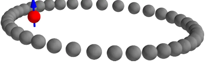
Figure 3.3: The system under consideration – a magnetic atom in a quantum corral.
1
Chapter 3. Signal Control and Transmission Using Magnetic Atoms 22
Our goal is to compute the Green’s function for the conduction electrons:
G(r,r0;t) =−iΘ(t)h{ψs(r;t), ψs†(r0)}i . (3.17) By carrying out the calculation, one obtains (Appendix G)
G(r,r0;ω) =G0(r,r0;ω) +G0(r,r0;ω)T(ω)G0(r0,r0;ω) . (3.18) In Eq. 3.18, G0(r,r0;ω) is the Green’s function of the QC (as derived in Chapter 2); fur-thermore, the influence of the MA is described by the T-matrix:
T(ω) =|χ|2G(ω) (3.19)
withG(ω)[=−iΘ(t)h{fs(t), fs†}i(ω)] being the impurity atom’s Green’s function.
Figure 3.4: The Kondo mirage. A magnetic impurity sits at the left focus of an elliptical
quantum corral. By subtracting off the local density of states of the corral with no impurity present one sees the presence of the magnetic atom (in the local density of states) around the filled focus; at the unfilled focus (on the right) a signal is also visible – the magnetic atom’s existence has been broadcast to the other end of the corral.
The quantity measured experimentally is the local density of states (LDOS), Eq. 2.2. [Recall that the LDOS is proportional to the differential conductance measured by an STM.[12]]
Chapter 3. Signal Control and Transmission Using Magnetic Atoms 23
atoms arranged in an ellipse, (x/a)2+ (y/b)2 = 1, where a/b= 1.5 witha= 8.583[nm] on a Cu(111) surface – EF = 0.45[eV] and m = 0.38me.[17, 18] We place the MA at one foci of the elliptical QC, f =√a2−b2.
Computing the LDOS using Eq. 3.18 gives the results in Figure 3.5. In the density plot, the
LDOS of the QC has been subtracted off to display the effect the MA has on the electronic properties of the system. As done in [17], a line of constant slope has been subtracted off the
LDOS data at both the filled and mirage focus. One readily verifies the agreement between our calculation and the experimental data.[17] At the site of the MA (the filled focus), a
prominent KR is observed in the electron density of states; this signal is the experimental signature of Kondo physics.[17] Furthermore, a clear KR is observed at the unfilled focus
(i.e. the mirage signal) in both spatial and energy sweeps of the LDOS. These results confirm that the theory we developed in the previous sections is suitable to describe the
physics contained in the mirage experiment.
Figure 3.5: The mirage signal. A single magnetic impurity sits at the left focus of a
Chapter 3. Signal Control and Transmission Using Magnetic Atoms 24
3.3
Signal Control and Transmission
The mirage experiment is particularly interesting because it exploits the electron’s spin degree of freedom. There is currently interest in exploring technologies that take advantage
of this intrinsic electron property (the field of spintronics).[32–35] The mirage experiment showed how the KR signal could be transmitted between spatially distinct points via the
eigenstates of the QC, but here we ask the question: can we control this signal?
Figure 3.6: Schematic for the proposed device. Using a metallic surface as the platform,
two magnetic impurities are to be placed inside of an elliptical quantum corral – one magnetic atom will be positioned on a focus; the other will be translated around inside the corral.
To this end, we consider the system shown in Fig. 3.6 – an elliptical QC with two MAs: the first MA is located at one focus of the QC with the other atom free to be moved about within
the walls of the corral. We describe the system by thetwo-impurity Kondo Hamiltonian
ˆ
H= ˆH0+ ˆV (3.20)
where ˆH0(= P n,s
εnc†n,scn,s) is the Hamiltonian of the bare system, and ˆV describes the coupling of the MAs to the 2DEG and to each other. The interaction between the MAs is taken into account by including the Ruderman-Kittel-Kasuya-Yosida (RKKY) interaction
in the potential.[29, 30, 36] Specifically,
ˆ
V =J1τ¯1·S(r1) +J2τ¯2·S(r2) +Kτ¯1·τ¯2 (3.21)
where ¯τiis the spin operator for MAi(located at positionri),S(ri)[= (1/2)P s,s0
ψs(† ri)¯σs,s0ψs0(ri)]
Chapter 3. Signal Control and Transmission Using Magnetic Atoms 25
RKKY interaction; namely, the effective interaction between the MAs via the 2DEG.[36]] In what follows, we will focus on the case of antiferromagnetic interimpurity interaction,
K >0.
Figure 3.7: The system under consideration – two magnetic atoms in a quantum corral.
In the two impurity Kondo problem, there are two important energy scales: the
single-impurity Kondo temperatureTK (Eq. 3.15) and the interimpurity interactionK. ForK
TK, the interimpurity interaction is unimportant and the system behaves as two independent impurities. ForK TK, the Kondo effect will be inhibited as the two impurities will lock into a singlet. In general, there is competition/interplay between the Kondo effect and the
interimpurity interaction.
Motivated by this physics, we treat Eq. 3.21 by employing a fermionic representation for
each MA’s spin operator:[28]
¯
τi= 1 2
X
s,s0
fi,s† σ¯s,s0fi,s0 (3.22)
where, as before, we have a constraint on the Hilbert space P s
fi,s† fi,s = 1. Then, the coupling between spin operators can be written as (Appendix F)
¯
τi·S(ri) =− 1 2
X
s,s0
[ψs†(ri)fi,s][fi,s† 0ψs0(ri)] + const. (3.23a)
¯
τ1·τ¯2 =− 1 2
X
s,s0
[f2,s† f1,s][f1,s† 0f2,s0] + const. (3.23b)
Chapter 3. Signal Control and Transmission Using Magnetic Atoms 26
effective Hamiltonian
ˆ
H =X n,s
εnc†n,scn,s+ 2 X i=1 " λi X s
fi,s† fi,s−χi X
s
fi,s† ψs(ri)−χ∗i X
s
ψs†(ri)fi,s #
−ΦX
s
f1,s† f2,s−Φ∗ X
s
f2,s† f1,s (3.24)
where the parameters{χi,Φ, λi}are determined (self-consistently) by
χi:=
Ji 2
X
s
hψs†(ri)fi,si (3.25a) Φ := K
2 X
s
hf2,s† f1,si (3.25b) X
s
hfi,s† fi,si= 1. (3.25c) The physical quantity of interest is once again the LDOS: A(r;ω) =−(1/π)Im[G(r,r;ω)] where G(r,r;ω) is the Fourier transform of the conduction electrons’ Green’s function (Eq. 3.17).[12] Computing the Green’s function yields (Appendix G)
G(r,r0;ω) =G0(r,r0;ω) + 2 X
i,j=1
G0(r,ri;ω) ˆTi,j(ω)G0(rj,r0;ω) (3.26) where G0(r,r0;ω) is the Green’s function of the QC (as derived in Chapter 2), ri is the position of MA i, and the T-matrix is ˆTi,j(ω) = [−iΘ(t)h{fi,s(t), fj,s† }i](ω)χ∗iχj.
Using the same structural and surface parameters as in the previous section (the case of a single MA in a QC), we introduce the second MA into the Green’s function via Eq. 3.26.
The LDOS for different distances between the MAs is shown in Fig. 3.8. In the density plot, the LDOS of the QC along with the off-focus MA is subtracted from the total electron
LDOS to emphasize the change in the mirage signal due to interference caused by the off-focus MA. Also, as done previously, a line of constant slope has been subtracted off the
LDOS data at the filled and mirage focus.
From the spatial (energy) sweep of the LDOS shown in the density (mirage) plot, it is clear
that the KR at the mirage focus can persist even in the presence of a second MA; thus, the superposition of many-body states due to each MA can coherently interfere. Remarkably,
Chapter 3. Signal Control and Transmission Using Magnetic Atoms 27
Figure 3.8: Signal control and transmission using magnetic atoms. Two magnetic atoms sit inside a quantum corral with one of the impurities located at the left focus of the corral. Top image: A spatial plot of the local density of states evaluated at the Fermi energy (with the density of states of the quantum corral and off-focus magnetic atom subtracted off). In this image one sees that the corral’s wave function has been modified by the presence of the second magnetic impurity (see Fig. 3.5); however, the Kondo mirage still persists. Bottom image: Energy sweep of the local density of statesA(r;ω) at the filled focus (left) and unfilled focus (right) for various position configurations. While doing little to the filled focus, small translations of the “free” magnetic atom greatly change the signal observed at the mirage focus. [Note: a line of constant slope has been subtracted off the bottom images.]
from an anti-resonance (black curve) to a resonance (red curve). The other coloured lines show the evolution of this signal as the off-focus MA is moved from a distance of 6.69[nm] (black curve) to 0.96[nm] (red curve) away from the filled focus MA. At the filled focus, the LDOS changes very little as the off-focus MA is relocated; however, the signal changes
drastically at the mirage focus. Hence, the two MA QC device can be thought of as a signal modulator[37] – the original KR signal at the mirage focus (due to the filled focus MA) is
Chapter 4
Atomic-Scale Engineering of
Superconducting Nanostructures
We now consider engineering superconducting nanostructures atom-by-atom. Our system is a metal film deposited on top of a bulk superconductor. As we will see in the ensuing
discussion, superconductivity is induced in the bulk states of the film via the proximity effect, but not the surface states – a two-dimensional electron gas persists on the surface.
However, an impurity atom on the surface strongly couples the surface state to the bulk states.[12] This process induces superconductivity in the region of the impurity, making the atom behave as asuperconducting impurity.
In this Chapter, we review key properties and features of superconducting systems and
introduce the concept of superconducting atoms; we then extend the scattering formalism to treat superconducting impurities. Finally, we discuss the engineering of superconducting
nanostructures and, in particular, display precise control over Andreev bound states.
Chapter 4. Atomic-Scale Engineering of Superconducting Nanostructures 29
4.1
Superconductivity
4.1.1 Background
When certain materials are cooled down below some critical temperature,Tc, they transition into the remarkable superconducting (SCing) state of matter.[38] A material in this phase
has zero electrical resistance or infinite conductance – i.e. the material superconducts. Besides electrical currents flowing unimpeded inside a SC, these materials also expel external
magnetic fields up to a small length called thepenetration depth.[39] Namely, the bulk of a SC is perfectly diamagnetic – a characteristic feature known as theMeissner effect1.[38, 40]
Fig. 4.1 shows the change in resistivity from the normal to SCing region as the temperature is lowered as well as the Meissner effect inside a SC slab of lengthL.
Figure 4.1: Defining properties of superconductors. Left image: The resistivity of a
superconductor, R vs. T – the resistivity is zero in the superconducting state (below the critical temperature Tc). Right image: The Meissner effect – when immersed in a weak
magnetic fieldB0, a superconductor expels the field in its bulk.
An acceptable microscopic theory of superconductivity did not emerge for nearly 50 years from its discovery in 1911 by Onnes[41, 42] to the theory developed by Bardeen, Cooper,
and Schrieffer (BCS) in 1957.[43] As such, in this intermediate period many physicists tried and failed to explain the phenomenon of superconductivity2.[42] However, prior to the
BCS theory, powerful phenomenological approaches emerged that could reproduce essential features of superconductors, namely the London and Ginzburg-Landau theories.[39, 44]
1
Note that the Meissner effect is different from Lenz’s law: the Meissner effect persists even in equilibrium, whereas Lenz’s law is a dynamical effect only.
2
Chapter 4. Atomic-Scale Engineering of Superconducting Nanostructures 30
To develop a meaningful microscopic theory of superconductivity it is essential to determine the operative physics. Namely, one must determine the essential interactions that account
for the features of a SC, but also what interactions can be safely disregarded in the Hamil-tonian. Several important discoveries/observations were made in the years leading up to
1957 that were crucial in making these choices.
First was the experimental discovery of the Isotope effect, where it was found that the
superconducting critical temperature (from the normal state to the SC state) was inversely proportional to the mass of ions in the underlying lattice: Tc∝1/
√
M.[45, 46] This result hinted that it would be necessary to consider interactions between conduction electrons and phonon excitations in the vibrating lattice. This coupling was first explored by Herbert
Fr¨ohlich3 in 1950[47] as well as Bardeen and Pines in 1955.[48]
Figure 4.2: An attractive interaction between electrons. An illustration of how two
electrons elude the repulsive Coulomb interaction via the lattice. Top image: The outgoing electron (on the left) creates a phonon. Bottom image: The incoming electron “feels” an attractive interactionat a later time due to the phonon.
It was determined that in certain systems, mediated by lattice vibrations, electrons are able to evade the repulsive Coulomb interaction.[39] The essence of this interaction is shown in
Fig. 4.2: an electron in the Fermi sea attracts nearby positively charged ions in the lattice; then, the resulting phonon excitation attracts another conduction electron. The net result is
that in such materials one can integrate out the Coulomb and electron-phonon interactions replacing them with an effectiveattractive electron-electron interaction.[49]
The final key insight came from the Cooper problem. In 1956, Leon Cooper considered the problem of two electrons interacting through an attractive interaction above a filled
3
Chapter 4. Atomic-Scale Engineering of Superconducting Nanostructures 31
noninteracting Fermi sea.[50] The electrons of momentum p1 and p2 (Fig. 4.3) interact with the Fermi sea only through the Pauli principle; i.e. only states with E > EF are available to the two electrons.
Figure 4.3: The Cooper problem – two electrons with momentap1andp2interact above
a filled noninteracting Fermi surface. The electrons form a bound state for an arbitrarily weak attractive interaction.
By considering the case of a spin-singlet with zero center-of-mass momentum one can show that the energy of the electron pair becomesE= 2EF−2∆ where ∆>0.[39] Therefore, two particles of opposite momentum and spin interacting near a filled Fermi surface will form a bound state for an arbitrarily weak attractive interaction, referred to as a Cooper pair
(Fig. 4.4). Therefore, the Fermi sea is unstable – a collection of electrons interacting through an arbitrarily weak attractive interaction will form (energetically favourable) Cooper pairs;
this results in an energygap between the ground state and the excited states.
Figure 4.4: Schematic of a Cooper pair – two electrons of opposite momentum (black
arrows) and spin (blue arrows) forming a bound state.
Equipped with these insights (affording a mechanism to produce the SCing state), BCS developed a successful microscopic theory of superconductivity in 1957.[43] Consequently,
they were awarded the Nobel prize in 1972.[51]
Chapter 4. Atomic-Scale Engineering of Superconducting Nanostructures 32
4.1.2 Superconducting Atoms
The defining traits of SCs (perfect conductance and diamagnetism) lend themselves to a
myriad of technological applications: SCing wires in power lines, strong magnetic fields for magnetic levitation, sensitive magnetometers, and more.[52–57] SCing structures built on the nanoscale – SCing nanostructures – further open up the potential for unique device
applications.[58–61]
In particular, there is interest in superconductivity on the atomic scale with experiments showing the state exists in atomically thin films,[62, 63] small chains of molecules,[64] and
isolated nanoparticles.[65] Such SCing nanostructures could be used to replace the ordinary conductors needed to fabricate interconnect wires in electronics.[64] Thus, a fundamental question arises: is there a limit to the number of atoms required to produce the many-body
SCing state? It turns out the answer is yes – a material ceases to superconduct below a certain size, namely when the system’s level spacing becomes comparable to the (bulk)
superconducting gap.[65–67] Here, we demonstrate a novel mechanism which allows one to circumvent this limit, enabling single atoms to exhibit superconducting properties; we
utilize this mechanism to create SCing nanostructures with a bottom-up approach.
An important, but subtle, feature of superconductivity and hence SCing nanostructures is
the proximity effect.[68] This effect occurs when a SC is placed in good electrical contact with a normal material; specifically, Cooper pairs tunnel from the SC to the normal material
inducingsuperconductivity.[68, 69] The induced SCing state only persists so far into the bulk of the normal material before it is lost and the sample retains its standard properties. Only
recently have the microscopic principles behind this effect been explored in detail.[69, 70]
As a result, one can consider the setup shown in Fig. 4.5 – a thin metal layer is deposited
on top of a bulk SC. For concreteness consider a Cu(111) film deposited on a SCing crystal, as this surface harbours a two-dimensional electron gas (2DEG). Because of the proximity
effect, superconductivity will be induced in the bulk of the film, but not on the surface. [Recall, surface electrons in Cu(111) are orthogonal to bulk electrons.] Furthermore, recall
that an impurity atom on the surface strongly couples the surface and bulk states.[12] Remarkably, this means an impurity can induce superconductivity at a specific location on
Chapter 4. Atomic-Scale Engineering of Superconducting Nanostructures 33
Figure 4.5: A superconducting atom. A thin metal film is deposited onto a bulk
su-perconductor. Due to the proximity effect, the bulk of the film becomes superconducting; because of the orthogonality between surface and bulk states, the surface remains normal. One can induce superconductivity on the surface through the addition of impurity atoms.
The effect of placing an impurity atom in this system will again be described by Eq. 1.2. Written explicitly in terms of Nambu spinors, one has
ˆ
V =UΨ†S(r0)τ3ΨS(r0) +C h
Ψ†S(r0)τ3ΨB(r0) + Ψ†B(r0)τ3ΨS(r0) i
(4.1)
where ΨS(r0) (ΨB(r0)) is the Nambu spinor for the surface (bulk) at the location of the
impurity, andτµ are Pauli matrices (in Nambu space).
4.2
Scattering Formalism: Superconducting Impurities
We start by considering a single SCing impurity on the metal surface at position r0. As discussed in Appendix E, an inert scatterer gives rise to a “scattering potential” of the form
ˆ
V =V0(ω)δ(ˆr−r0) where ˆris the electron position operator and
V0(ω) = 1
πρ0
Q D
D Q
(4.2)
withρ0 being the surface electron density of states and
Q=Cp −(ω+iΓ)
∆2−(ω+iΓ)2 (4.3a)
D=Cp −∆
∆2−(ω+iΓ)2 . (4.3b)
Chapter 4. Atomic-Scale Engineering of Superconducting Nanostructures 34
The Green’s function for this system is obtained from the Dyson equation:
G(r,r0;ω) =G0(r,r0;ω) +G0(r,r0;ω)V0(ω)G(r0,r0;ω) (4.4) whereG0(r,r0;ω) is the bare Green’s function of the 2DEG. [Note: for a SCing system, the Green’s function is a 2x2 matrix (Appendix C).] To solve Eq. 4.4, first let r=r0. One can then find an expression for G(r0,r0;ω) which can be placed back into Eq. 4.4 to obtain
G(r,r0;ω) =G0(r,r0;ω) +G0(r,r0;ω) ˆT(ω)G0(r0,r0;ω) (4.5) where the T-matrix has been defined as
ˆ
T(ω) :=V0(ω)[I−G0(r0,r0;ω)V0(ω)]−1. (4.6) To proceed, it is useful to know that the bare Green’s function of a 2DEG is (Appendix D)
G0(r,r0;ω) =
G011(r,r0;ω) 0 0 G022(r,r0;ω)
. (4.7)
The elements of the bare Green’s function are
G011(r,r0;ω) = (
−i(πρ0)H0(1)(k+|r−r0|) ,r6=r0
−i(πρ0) +ρ0ln
EF+ω
D−ω
,r=r0
(4.8a)
G022(r,r0;ω) = (
−i(πρ0)H0(2)(k−|r−r0|) ,r6=r0
−i(πρ0)−ρ0ln
EF−ω
D+ω
,r=r0
(4.8b)
wherek2±= 2m(EF ±ω),ρ0 is the 2D electron density of states, Dis an ultraviolet cutoff, and H0(i) is a Hankel function.[26]
Now, consider a collection of SCing impurities on the surface of the thin metal film. The
Hamiltonian of the system is ˆH= ˆH0+ ˆV where ˆH0 is the Hamiltonian of the system in the absence of the the SC impurities (i.e. a 2DEG) and ˆV is the “scattering potential” arising from the coupling of the impurity atoms to the bulk SC as a result of the proximity effect. Namely, the single-body operator is ˆV =V0(ω)P
i
Chapter 4. Atomic-Scale Engineering of Superconducting Nanostructures 35
The Green’s function is obtained from the Dyson equation (Eq. 2.8). Integrating over the delta functions gives
G(r,r0;ω) =G0(r,r0;ω) +X i
G0(r,ri;ω)V0(ω)G(ri,r0;ω) (4.9) where G0(r,r0;ω) is the system’s bare Green’s function. To move forward, it will prove useful to write the sum above as a matrix multiplication. It is straightforward to show
G(r,r0;ω) =G0(r,r0;ω) +G T
0(r;ω) ˆV(ω)G(r0;ω) (4.10) where we have introduced the vectors
G(r;ω) :=
G11(r1,r;ω) G12(r1,r;ω)
G11(r2,r;ω) G12(r2,r;ω) ..
. ...
G21(r1,r;ω) G22(r1,r;ω)
G21(r2,r;ω) G22(r2,r;ω) .. . ...
, G0(r;ω) :=
G011(r1,r;ω) 0
G011(r2,r;ω) 0 ..
. ...
0 G022(r1,r;ω) 0 G022(r2,r;ω)
.. . ... (4.11)
withGij(r,r0;ω) being a matrix element of the Green’s function and introduced the potential matrix defined as
ˆ
V(ω) := 1
πρ0
Q 0 . . . D 0 . . .
0 Q . . . 0 D . . .
..
. ... . .. ... ... ...
D 0 . . . Q 0 . . .
0 D . . . 0 Q . . .
.. . ... . .. ... ... ... . (4.12)
[Note: above we utilized that G0(r,r0;ω) = G0(r0,r;ω).] It is our intention to obtain an explicit expression for the Green’s function from the Dyson equation. To that end, we
Chapter 4. Atomic-Scale Engineering of Superconducting Nanostructures 36
and arranging the result as a matrix yields
G(r0;ω) =G0(r0;ω) + ˆG0(ω) ˆV(ω)G(r0;ω) (4.13) where we have defined the matrix
ˆ
G0(ω) :=
G011(r1,r1;ω) G110 (r1,r2;ω) . . . 0 0 . . .
G011(r2,r1;ω) G110 (r2,r2;ω) . . . 0 0 . . . ..
. ... . .. ... ... . ..
0 0 . . . G022(r1,r1;ω) G022(r1,r2;ω) . . . 0 0 . . . G022(r2,r1;ω) G022(r2,r2;ω) . . . .. . ... . .. ... ... . .. . (4.14)
Rearranging Eq. 4.13 gives an explicit equation for the vector of Green’s functions:
G(r0;ω) = h
I−Gˆ0(ω) ˆV(ω) i−1
G0(r0;ω). (4.15) Inserting Eq. 4.15 into the Dyson equation returns the Green’s function. Namely,
G(r,r0;ω) =G0(r,r0;ω) +GT0(r;ω) ˆT(ω)G0(r0;ω) (4.16) where the T-matrix has been defined as
ˆ
T(ω) := ˆV(ω)hI−Gˆ0(ω) ˆV(ω) i−1
. (4.17)
4.3
Engineering Superconducting Nanostructures
Equipped with this formalism, we are now in a position to consider atomically engineered SCing nanostructures. Recall that in quantum systems closed geometries lead to discrete
states; in SCing systems, such states are known asAndreev bound states (ABS).[71, 72] To that end, we consider an elliptical quantum corral (QC) constructed using SC impurities –
Chapter 4. Atomic-Scale Engineering of Superconducting Nanostructures 37
Figure 4.6: Atomically engineered superconducting nanostructure. The system is most
directly probed using a scanning tunneling microscope with a superconducting tip.
To investigate this system, consider the configuration shown in Fig. 4.6. Here, we probe the nanostructure using a scanning tunneling microscope (STM) built with a SCing tip. We are
interested in computing experimentally observable quantities of the SCing system. To that end, it can be shown that the tunneling current between the surface and the STM tip is
given by the superposition of currents from single-particle tunneling and pair tunneling;[73] the current due to pairs, known as theJosephson current, is a signature of the SCing state.
The amplitude of the dc Josephson current is given by4
JS =
G0
πe∆
∞
Z
0
dω Im
fnanoret (ω)−fnanoret (−ω)
FSTM(ω; ∆) (4.18)
where G0(= e24πρnanoρSTMT02) is the normal state conductance between the STM and the surface withρnano (ρSTM) being the nanostructure’s (STM’s) electron density of states (evaluated at the Fermi energy) and with T0 being the matrix element for an electron to tunnel from STM to surface, ∆ is the SCing gap of the STM tip,fnanoret (ω)[=G12(r,r;ω)/πρ0] is the dimensionless anomalous (retarded) function of the nanostructure, and
FSTM(ω; ∆) =
( 2
√
∆2−ω2 arctan
√ ∆2−ω2
ω+∆
,|∆|>|ω|
1
√
ω2−∆2 ln
ω+∆+√ω2−∆2
ω+∆−√ω2−∆2
,|∆|<|ω|
. (4.19)
Similar to experiments, we consider the following structural and material properties for the QC: 44 impurity atoms arranged in an ellipse, (x/a)2+ (y/b)2 = 1, where a/b = 2 with a = 7.92[nm] on a Cu(111) surface – EF = 450[meV] and m = 0.38me;[17, 18] For simplicity, we consider the case where both the material inducing superconductivity on the
surface and the STM tip are the same (e.g. niobium) – ∆nano= ∆STM≈2[meV].
Chapter 4. Atomic-Scale Engineering of Superconducting Nanostructures 38
We compute the Green’s function of the QC from Eq. 4.16. To do this, we must assign numeric values to the broadening and ultraviolet cutoff. It is reasonable to take Γ≈0.01∆ andD≈EF. Computing the amplitude of the system’s Josephson currentJS as a function of position (via Eq. 4.18) results in the plot shown in Fig. 4.7.
Figure 4.7: Josephson current for a superconducting quantum corral. The blue (red)
regions represent areas of high (low) current with white regions being in-between. Regions outside the corral have minimal signs of superconductivity, whereas regions with tightly packed superconducting impurities exhibit a large Josephson current.
An initial observation is that we do obtain a Josephson current – the impurities are indeed inducing superconductivity on the surface of the metal. Also, much like the QCs built with
“ordinary” impurities, standing wave patterns emerge inside the wall of the SCing QC; however, here these standing waves are ABS. Thus, the SCing QC is capable of confining/
harbouring ABS – this confinement is not perfect though, as we do not have a solid wall.
Therefore, we have demonstrated how to control superconductivity on the scale of single
atoms; furthermore, we have shown that confinement gives rise to ABS. Now, we seek to control the ABS inside the QC. To that end, we consider the single-atom gating techniques
used in [18]; namely, by translating a single SCing impurity inside the SCing QC, we seek to modify the particle/hole wave functions of the system. We will observe such changes
by computing the local density of states (LDOS) – for a SCing system Eq. 2.2 becomes