ABSTRACT
IYER, BALAJI VISWANATHAN. Length Adaptive Processors: A Solution for the
Energy/Performance Dilemma in Embedded Systems. (Under the direction of Dr. Thomas M. Conte).
Embedded-handheld devices are the predominant computing platform today. These
devices are required to perform complex tasks yet run on batteries. Some architects use ASIC
to combat this energy-performance dilemma. Even though they are efficient in solving this
problem, an ASIC can cause code-compatibility problems for the future generations. Thus, it
is necessary for a general purpose solution. Furthermore, no single processor configuration
provides the best energy-performance solution over a diverse set of applications or even
throughout the life of a single application. As a result, the processor needs to be adaptable to
the specific workload behavior. Code-generation and code-compatibility are the biggest
challenges in such adaptable processors.
At the same time, embedded systems have fixed energy source such as a 1-Volt
battery. Thus, the energy consumption of these devices must be predicted with utmost
accuracy. A gross miscalculation can cause the system to be cumbersome for the user.
In this work, we provide a new paradigm of embedded processors called Dynamic
Length-Adaptive Processors that have the flexibility of a general purpose processor with the
specialization of an ASIC. We create such a processor called Clustered Length-Adaptive
Word Processor (CLAW) that is able to dynamically modify its issue width with one VLIW
instruction overhead. This processor is designed in Verilog, synthesized, DRC-checked, and
transistor-level analysis tools to dispel several myths that were thought to be dominating
factors in embedded systems.
To compile benchmarks for the CLAW processor, we provide the necessary software
tools that help produce optimized code for performance improvement and energy reduction,
and discuss some of the code-generation procedures and challenges.
Second, we try and understand the code-generator patterns of the compiler by
sampling a representative application and design an ISA opcode-configuration that helps
minimize the energy necessary to decode the instructions with no performance-loss. We
discover that having a well designed opcode-configuration, not only reduces energy in the
decoder by also other units such as the fetch and exception units. Moreover, the sizable
amount of energy reduction can be achieved in a diverse set of applications.
Next, we try to reduce the energy consumption and power-dissipation of register-read
and register-writes by using popular common-value register-sharing techniques that are used
to enhance performance. We provide a power-model for these structures based on the value
localities of the application. Finally, we perform a case-study using the IEEE 802.11n PHY
Transmitter and Decoder and identify its energy-hungry units. Then, we apply our techniques
and show that CLAW is a solution for such hybrid complex algorithms for providing
Length Adaptive Processors: A Solution for the Energy/Performance
Dilemma in Embedded Systems
by
Balaji Viswanathan Iyer
A dissertation submitted to the Graduate Faculty of North Carolina State University
in partial fulfillment of the requirements for the degree of
Doctor of Philosophy
Computer Engineering
Raleigh, North Carolina
2009
APPROVED BY:
_______________________________ ______________________________
Dr. Thomas M. Conte Dr. Eric Rotenberg
Committee Chair
DEDICATION
BIOGRAPHY
Balaji was born in Thrissur, India on December 16, 1980. He is the only child of T. N. and
Geetha Viswanathan. He immigrated to USA at the age of 11 with his parents. Balaji
completed his Bachelors Degree in Computer Engineering at Purdue University, West
Lafayette, Indiana in 2002. Later on, he received his Masters in Electrical Engineering from
North Carolina A&T State University under the direction of Dr. John Kelly in 2003. After
ACKNOWLEDGMENTS
I would like to thank my advisor, Dr. Thomas M. Conte for being a great research
advisor. His support, guidance and encouragement have helped me gain an enormous amount
of knowledge and accomplish my PhD. I will be forever thankful toward him. I would also
like to thank my committee members, Dr. Eric Rotenberg, Dr. Purush Iyer and Dr. W. Rhett
Davis for their advice and encouragement on this journey.
I would further like to thank Dr. Davis and his students, Ravi Jenkal, Ambrish Sule
and Hao Hua for helping me with EDA tools and scripts. I am forever thankful for their time
and assistance with helping me synthesize and simulate my processor and do power
measurements using NCSU Cadence and Synopsys tools. Further thanks go to Meeta Yadav,
Thorlindur Thorolfsson, Monther Aldwairi, Manav Shah, and Shobhit Kanujia for helping
me start the CLAW project. I would like to thank Chad Rosier and Liang Han for helping me
with the GCC compiler.
In addition, my friends at CESR and NCSU: Mark Dechene, Mawuya Alotoom, Niket
Choudhri, Aravindh Anantharaman, Ali El-Hajj Mahmood, Vimal Reddy, Ahmed Alzwawi,
George Patsilaras, Yuentao Peng, Salil Pant, Liang Han, Mazen Kharboutli, Siddhartha
Chabrra, Devesh Tiwari, J. Elliot Forbes, Hashem Hashemi, Zane Purvis, Tongtong Chen,
Hanyu Cui, Fei Gao, Fei Guo, Sabina Grover, Palomi Pal, Chungsoo Lim, Shaolin Peng,
Zentao Hu, Sibin Mohan, Radha Venkatagiri, etc., have helped me both academically and
I would also like to thank the present and former TINKER members: Shobhit
Kanujia, Saurabh Sharma, Jesse Beu, Paul Bryan, Chad Rosier, Jason Poovey, Milind
Nemlekar and Sajjid Reza who have supported me in my research and provided me quality
insights and helped me relax when things got unbearable. Additional thanks go to Jason for
helping me proof-read my thesis proposal and several of my papers.
This section will be incomplete if I did not acknowledge the people who have helped
me get up to this level. My sincere thanks go to Dr. John Kelly Jr. for providing me
encouragement to pursue a PhD and for being a great MS advisor. Similarly, thanks go to my
two high-school Mathematics teachers (Mr. Randy Zamin and Mr. Bruce Thornquist) and my
Chemistry teacher (Mr. Mayfield) who has helped me uncover my Math and Science abilities
and showed me the light toward this career path.
Mrs. Sandy Bronson has greatly helped me on the administrative side by making sure
my paperwork is turned on to the right person at the right time. Thank you very much Mrs.
Bronson!
Finally, my family has offered a great deal of support and encouragement in my life. I
want to individually thank my loving father (T. N. Viswanathan) and mother (Geetha
Viswanathan). Finally, I would like to acknowledge my loving fiancée Gayathri.
TABLE OF CONTENTS
LIST OF TABLES ...viii
LIST OF FIGURES ...ix
Chapter 1 Motivation ...1
1.1 Related Work...3
1.1.1 Opcode-Optimization...4
1.1.2 Register-Sharing ...5
1.1.3 Application-Aware Processor Customization ...6
1.1.4 Next-PC Computation for Clustered Architectures ...13
1.1.5 Clustered Microarchitecture Scheduling...10
1.2 Dissertation Layout...14
Chapter 2 Experimental Framework...15
2.1 The CLAW Architecture...16
2.2 Top-Level Architecture...17
2.2.1 Fetch Unit. ...18
2.2.2 Decode (or Dispatch), Execution and Write Back Units ...18
2.3 Integrating Multiple Clusters ...20
2.3.1 Register-File Organization ...21
2.4 Multithreading Architecture...22
2.5 Compiler Support for CLAW...24
2.5.1 GCC toolchain for CLAW ...24
2.6 Benchmarks...24
2.7 Analysis Framework...26
Chapter 3 Instruction-width optimization ...29
3.1 Dynamic Issue-Width Scalability...30
3.2 Pipeline Clock-Gating...31
3.3 Next PC Calculation ...34
3.4 Instruction Scheduling and Shutoff Insertion...35
3.5 Results...40
3.5.1 Base Results...40
3.5.2 Dynamic Length-Adaptivity...47
3.6 Conclusion...62
Chapter 4 Opcode Optimization ...64
4.1 Popular ISA Encoding in Existing Embedded Systems ...66
4.3 Results...71
4.4 Multi-cluster CLAW Configurations...80
4.5 Conclusion...83
Chapter 5 Register-Sharing ...84
5.1 Preliminary Analysis...85
5.2 Register Sharing Techniques...85
5.3 Experiments and Terminology ...88
5.4 Results...89
5.5 Conclusion...99
Chapter 6 A Case study on IEEE 802.11n PHY...100
6.1 Motivation ...100
6.2 IEEE 802.11n Architecture ...101
6.2.1 FEC Transmitter and Decoder...103
6.2.2 Interleaving and De-interleaving ...104
6.2.3 OFDM Symbol Mapping ...105
6.2.4 MIMO Encoding and Decoding ...106
6.2.5 Fast Fourier Transform ...108
6.3 Implementation...108
6.4 Results...110
6.4.1 Instruction Distribution ...110
6.4.2 Parallelism ...112
6.4.3 Energy Consumption...113
6.5 Conclusion...116
Chapter 7 Conclusion and Future-Work ...118
LIST OF TABLES
Table 2-1: Register Functions...22
Table 2-2: Toolchain Components...24
Table 2-3: EEMBC Benchmarks Description ...26
Table 4-1: Original CLAW Encoding...65
Table 4-2: Encoded to Reduce Hamming Distance ...65
Table 4-3: Illustration of Distance Saved using Source Register Switching...71
Table 4-4: Percentage Dynamic Energy Reduction...73
Table 4-5: Percentage Static Energy Reduction ...74
Table 4-6: Different Load Instruction Types in CLAW ...78
Table 4-7: Percentage Dynamic Energy Reduction ( 2 Cluster CLAW) ...80
Table 4-8: Percentage Static Energy Reduction (2 Cluster CLAW) ...81
Table 4-9: Percentage Dynamic Energy Reduction (4-Cluster CLAW)...82
Table 4-10: Percentage Static Energy Reduction (4-Cluster CLAW) ...82
Table 5-1: Zero and Duplicate writes for different register file configurations ...85
Table 6-1: Three Transmission Scenarios Example ...108
LIST OF FIGURES
Figure 1-1: OptimoDE, Tensilica, Lx and CLAW Design Flow...8
Figure 1-2: Steps for adding new Application into OptimoDE, Tensilica, Lx and CLAW...8
Figure 2-1: Power Delay Product of Some-Popular Embedded Processors ...17
Figure 2-2: CLAW Top-level Architecture...18
Figure 2-3: Clustered CLAW Block Diagram...21
Figure 2-4: CLAW Instruction Granularities ...21
Figure 2-5: CLAW Multithreading Flow-Diagram ...23
Figure 2-6: EEMBC Benchmark Structure ...25
Figure 2-7: Power Analysis Steps...27
Figure 2-8: Running an Executable on CLAW ...28
Figure 3-1: Shutoff Instruction Format ...31
Figure 3-2: Overall Clock Gating Circuit Block Diagram...32
Figure 3-3: Clock Gating Logic...32
Figure 3-4: Cascaded CLK Output ...33
Figure 3-5: Design-Flow of UAS Algorithm on GCC...36
Figure 3-6: Example of an Empty Cluster (marked in blue box) ...38
Figure 3-7: Cluster-Shutoff Algorithm ...39
Figure 3-8: Execution-time for 1-Cluster CLAW...41
Figure 3-9: Speedup of 2-Cluster CLAW over 1 Cluster Machine ...41
Figure 3-10: Speedup of 4 Cluster CLAW over 1 Cluster CLAW Machine ...42
Figure 3-11: Percentage of Copy Instructions in 2-Cluster CLAW Machine ...43
Figure 3-12: Percentage of Copy Instructions for 4-Cluster CLAW Machine...43
Figure 3-13: Dynamic and Static Energy or 1 Cluster CLAW...45
Figure 3-14: Dynamic Energy Values for a 2-Cluster CLAW Processor...46
Figure 3-15: Dynamic Energy Values for a 4-Cluster CLAW Processor...46
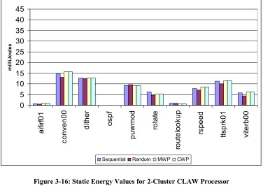
Figure 3-16: Static Energy Values for 2-Cluster CLAW Processor...47
Figure 3-17: Static Energy Values for 4-Cluster CLAW Processor...47
Figure 3-18: Dynamic Energy Distribution Function-Level Shutoff Insertion...48
Figure 3-19: Static Energy Distribution Function-Level Shutoff Insertion ...49
Figure 3-20: Dynamic Energy Distribution BB-Level Shutoff Insertion ...50
Figure 3-21: Static Energy Distribution BB-Level Shutoff Insertion...51
Figure 3-22: WriteOut function from Puwmod01 ...52
Figure 3-23: Control Flow Graph of WriteOut...53
Figure 3-24: CFG using Treegions in WriteOut...54
Figure 3-25: CFG using Treegions for ZtableLookup in Ttsprk01 ...55
Figure 3-26: Calculating Cluster Usage for Each Region...56
Figure 3-27: Shutoff Insertion at Treegion-level algorithm...57
Figure 3-29: Dynamic Energy Consumption for Region-Level Shutoff ...60
Figure 3-30: Static Energy Consumption with Region-level Shutoff...60
Figure 3-31: Dynamic Energy Consumption with BB-level Shutoff with Redundant Shutoff Removal...61
Figure 3-32: Static Energy Consumption with BB-level Shutoff with Redundant Shutoff Removal...62
Figure 4-1: Parallel Approach to Decode an OR instruction ...66
Figure 4-2: Serial Approach to Decode OR instruction...67
Figure 4-3: Opcode Optimization Algorithm ...69
Figure 4-4: Flow-Diagram of our Methodology...71
Figure 4-5: Base Energy Values for the Benchmarks...72
Figure 4-6: Dynamic EnergySavings in Each Unit of OSPF ...75
Figure 4-7: Dynamic Function-calls in Each Benchmark ...76
Figure 4-8: Number of Distinct Instruction Chains achieving 50% coverage ...78
Figure 5-1: Top-level block diagram of the map-table/map-vector...86
Figure 5-2: Flow-Diagram for the Writeback Stage ...87
Figure 5-3: Flow-diagram of the Register-Read Stage ...87
Figure 5-4: Different Placements of Zero-Writes...89
Figure 5-5: Power Dissipation for Random Register-Write (Reg. File Size = 16)...90
Figure 5-6: Power Dissipation for Random Register-Write (Reg. File Size = 32)...90
Figure 5-7: Power Dissipation for random Register-Write (Reg. File Size = 64)...91
Figure 5-8: Power Dissipation for random Register-Write (Reg. File Size = 128) ...92
Figure 5-9: Power Dissipation for random Register-Write (Reg. File Size = 256) ...92
Figure 5-10: Power Dissipation for Sequential Writes (Reg. File Size = 16) ...93
Figure 5-11: Power Dissipation for Sequential Writes (Reg. File Size = 32) ...94
Figure 5-12: Power Dissipation for Sequential Writes (Reg. File Size = 64) ...94
Figure 5-13: Power Dissipation for Sequential Writes (Reg. File Size = 128) ...95
Figure 5-14: Power Dissipation for Sequential Writes (Reg. File Size = 256) ...96
Figure 5-15: Power Dissipation for Seq-int writes (Reg. File Size = 16) ...96
Figure 5-16: Power Dissipation for Seq-int writes (Reg. File Size = 32) ...97
Figure 5-17: Power Dissipation for Seq-int writes (Reg. File Size = 64) ...97
Figure 5-18: Power Dissipation for Seq-int writes (Reg. File Size = 128) ...98
Figure 5-19: Power Dissipation for Seq-int writes (Reg. File Size = 256) ...98
Figure 6-1: IEEE 802.11N Transmitter...102
Figure 6-2: IEEE 802.11N Receiver ...103
Figure 6-3: Convolutional Transmitter [171] ...104
Figure 6-4: Block Interleaving [137] ...105
Figure 6-5: Alamouti Scheme (2 Transmit and 2 Receiver Antennas) [3] ...107
Figure 6-6: Dynamic Instruction Distribution of 802.11n Transmitter...110
Figure 6-7: Dynamic Instruction Distribution of 802.11n Receiver...111
Figure 6-8: Static Energy Dissipation for 2 Cluster CLAW ...114
Figure 6-9: Dynamic Energy Dissipation for 2 Cluster CLAW ...114
Chapter 1
Motivation
For the past decade portable handheld devices have gained significant popularity. These
embedded devices are now required to perform several complex tasks that were once only
attempted by high-performance systems [113] [147]. For example, a mobile-phone today
sends and receives voice, captures images and video, maintains a daily-planner, sends and
receives textual information, etc. Additionally, these devices must give high performance
while executing these applications [16] [56] [79] [113] . In order to be easily portable, they
must draw their power from a battery. Therefore, it is necessary for these embedded handheld
devices to give comparable performance with a high-performance system, yet consume
significantly less power and energy [56] [79] [113].
To tackle this problem, designers have discovered two broad solutions. If the architect is
aware of applications that are to be run on the system, then several processor optimizations
can be done such as inserting specialized units to perform a certain task faster (for example, a
unit that does discrete cosine transform for a image processing system), have specialized
instruction widths, etc. These processors are called Application-Specific Integrated Circuits
(ASIC). A well-designed ASIC can provide a significant performance boost while still
consuming a low amount of power. On the other hand, when a new application is introduced
into the system the ASIC must be re-designed, which can be prohibitively expensive and
In embedded systems, some applications are executed more frequently than others [147].
For example, in a music player such as iPod, the audio and video codec are executed more
frequently than the calendar application. Engineers can take a general purpose processor that
is able to execute a wide variety of application and tailor it for speeding up certain
algorithms. These processors can provide high-performance and still consume less-energy.
These tailored processors, unlike high-performance systems, are generally simpler and
require significant help from the compiler for scheduling, branch-prediction and so-forth
[16]. Sometimes, the availability of vast number of optimizing compilers, assemblers, etc. for
such architecture is limited [123]. Many embedded processor users are generally restricted to
a single compiler. By understanding the trends of this compiler in code-generation and
scheduling, one can optimize the appropriate processor units accordingly to greatly increase
performance and reduce power dissipation.
Even though such tailored processors seem to provide a flexible solution for embedded
systems, diverse characteristics among embedded applications and diversity within an
application make it impossible to select one processor configuration that is suitable for
providing optimal energy-performance solution.
Fisher, Faraboschi and Desoli in the year 1998 are the first researchers to understand this
concept and they tried to design a processor based on the application characteristics [48].
After a few years, three more processors emerged that have tried to find this optimal
processors. All these processors provide a static solution for finding this optimal ratio. When
a new application is introduced the processor must be remanufactured to gain this optimum.
In this dissertation, we provide a dynamic approach to reach this energy-performance
optima. This work illustrates a bottom-up approach to design a processor that will give the
optimal energy-performance ratio by examining the compiler and the target application. We
try to uncover some of the limitations the compiler imposes on the processor and propose to
design (or modify) the processor accordingly.
The processor is designed such that the binaries compiled using this code-generator is
able to obtain the highest performance for the energy budget. The end result of this thesis is a
circuit-level processor and an optimizing-compiler “couple” that tries to minimize power and
energy consumed by the processor without any performance loss. The main areas focused in
this work are ISA encoding optimization, register-sharing based on value locality, dynamic
and static data-path modification, and a power-aware scheduling algorithm.
In this work, energy is used as a metric because it is directly proportional to battery life
and it is more dependent on the workload than the processor frequency. Similarly, when we
speak of performance, we mean the number of cycles the program takes to execute in the
processor.
1.1 Related Work
the related work for opcode-optimization. Sections 1.1.2 and 1.1.3 discuss the related work
for register-sharing and width modification. The previous work in
instruction-scheduling algorithms and branch handling are explained in sections 1.1.4 and 1.1.5.
1.1.1 Opcode-Optimization
Tiwari, Malik and Wolfe in [148] and Tiwari, et al. in [149] describe ways to reduce
power by modifying the number of switching in software. They give a detailed description of
instruction level power reduction techniques for a specific set of applications. We extend this
idea to find some general power reduction schemes for a broad range of applications using
one application as a training set.
Kim and Kim in [75] and, Woo, Yoon and Kim in [155] describe a method for
reducing the Hamming distance between adjacent instructions. Unlike our work, they do not
mention the effects of their modifications on the power dissipation of the decoder or the
processor. They detail all of their work in switching activity, and neglect other metrics such
as power consumption or the wire-length of a processor component such as the instruction
decoder. Additionally, they do not analyze a single application or subset of applications,
rather they sample all applications that are run on the system to find the optimal encoding.
Varma et al. in [151] study the power reduction of switching in the register bus and the
bypass logic for the Intel XScale embedded processor. They indicate that switching in the
register port increased the instruction energy by 10%. Also, Haga et al. in [56] explore
dynamically assigning function units to reduce switching. They present a 26% power
In [112] Pechanek, Larin and Conte present a technique for entropy based encoding of
the ISA. The primary focus of this work is variable size instructions which frequently occur
in DSP architecture. Kalambur and Irwin in [72] study ways to reduce data fetch energy by
adding an addressing mode for ALU instructions to access operands from memory.
1.1.2 Register-Sharing
Optimizing register-usage for improving performance has been studied for the past two
decades. However the problems concerning power and heat dissipation in processors became
a problem starting in the nineties. Zyuban and Kogge in [164] study the power dissipation of
an integer register-file. Their models express the power consumption of a register in terms of
the number of read-write ports and issue width. Similarly, Zhao and Ye in [161] also provide
models for finding power dissipation in register-file.
Hu and Martonosi in [62] find that most read and write operations occur within a few
cycles. They introduce a value aging buffer that saves recently-produced values so that the
instructions requiring these values need not access them from register-file. They received a
power reduction of 30% with less than a 5% performance loss.
Kim and Mudge in [76] observed that only 0.1% of the cycles fully utilize a 16-bit read
port. The aim of their work was to reduce the number of read ports, not the number of
registers. They used a delay-writeback queue, an operation prefetch buffer and request
queues. Their results showed a 22% reduction in energy per register access.
Gonzalez et al. in [55] explained ways to share partial values between registers inside a
Ayala, Veidenbaum and Lopez-Vallejo in [8] proposed ways to statically find periods where
registers are not used and turn them off to reduce power. Using their method, they found a
46% total energy reduction in the entire MiBench benchmark suite.
Seznec, Toullec and Rouchecouste in [133] proposed that restricting certain function
units to write and read only a subset of registers (clustering the processor) can reduce the
access time by 33% and power by 50%. Jain et al. in [65] evaluates the register-file for an
ASIP. They use ARM7TDMI as a test processor. It is shown from their research that there
exists a high correlation between performance improvement and energy consumption. They
also showed that a slight increase in the number of registers gives a huge amount of power
reduction in ASIP (~50%).
Balakrishnan and Sohi in [10] discussed using a map-table for reducing physical
register pressure by sharing values such as ‘0’. Tran et al. in [150] proposed a way to mark
the reorder-buffer with one bit (this can be thought of as a bit-vector) to indicate if the
instruction’s result was a zero. Tran et al. also discusses using a map-table as a possibility.
These two papers are quoted extensively for value sharing inside the register-file to improve
performance. However, these papers do not mention the power implications of these
structures on the processor or the register file. We study their power effects and come up
with a power-model for these structures.
1.1.3 Application-Aware Processor Customization
The idea of customizing a general-purpose processor for an application was first
adaptability like CLAW are the Lx [46], Tensilica Xtensa LX2 [175] and the OptimoDE
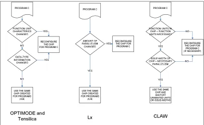
processors [34]. Figure 1-1 shows the design process of Lx, OptimoDE, Tensilica and
CLAW (assuming we are designing the processor to target programs A and B). The only
major difference between OptimoDE and Tensilica is that OptimoDE allows the user to fully
customize the instructions, while Tensilica uses a standardized ISA [33].
Lx architects provide a framework that analyzes a benchmark (or a set of benchmarks)
and design a processor with appropriate issue-width, function-units, etc. to maximize the
processor performance using the appropriate energy budget. OptimoDE framework tries to
analyze the source-code and provide hints to the user regarding the optimal issue-width,
function-units, data-path sizes, etc. Standard function units are inserted by the tools, but
custom-units must be hand-generated.
The biggest drawback for Lx, Tensilica and OptimoDE is they are static approaches.
Let’s assume we are trying to add a new application (‘C’) into the processors designed in
Figure 1-1. As shown in Figure 1-2, the processors must be redesigned for optimal
functioning, which can be expensive and time-consuming. This problem is overcome in
CLAW by providing mechanisms to dynamically adapt issue-widths and function-unit sizes
PROGRAMS {A, B} PROFILE AND EXTRACT REVELANT PARAMETERS FUNCTION UNIT UTILIZATION. DATA TYPE INFORMATION CREATE CUSTOM PROCESSOR (OPTIMODE X) PROGRAMS {A, B}. PROFILE AND EXTRACT PARALLELISM INFO CAPTURE THE ISSUE-WIDTH NECESSARY CREATE CUSTOM PROCESSOR (‘n’ ISSUE Lx)
PROGRAM A PROFILE AND EXTRACT REVELANT PARAMETERS EMBED THE PARAMETERS INTO THE EXECUTABLE
PROGRAM B PROFILE AND EXTRACT REVELANT PARAMETERS EMBED THE PARAMETERS INTO THE EXECUTABLE THE HARDWARE DYNAMICALLY SCALES THE ISSUE WIDTH AND
SHUTS OFF UNWANTED FUNCTION UNITS OPTIMODE and Tensilica Lx CLAW
To do the dynamic modification of issue width, the most successful method employed
by several high-performance configurable processors is gating the clock for the unused units
[61] [89] [97] [91] [118]. The granularity of a unit can be a specific gate [18], a function-unit
[9] [118] [61] [67], processor-stage [63] [91] [87] [89], or an entire cluster [97] [19]. Each of
the methodologies described can be beneficial, depending on the application. The key
question is at what part of the program must the gating occur so that optimal energy is
consumed with virtually no performance degradation? We provide the answer to this using
our CLAW software-framework.
In the past, several super-scalar researchers have studied this problem. In out-of-order
dynamic-scheduling processors, however, this problem is trivial because the processor has
direct control of the scheduling. Buyuktosunoglu, et al. [20] provides an adaptive issue queue
for reducing processor power. Albonesi [6] provides a methodology to dynamically shut off
units and processor issue-widths in super-scalar processors to save power. S. Rele et al. in
[119] have provided a mechanism to shutoff idle function-units in superscalar processors
using a profiling compiler. Unfortunately, dynamic-scheduling processors are not
energy-efficient for embedded systems. As per our calculations and comparisons with [165], for the
same transistor technology, the scheduling logic of a superscalar alone took more power than
an entire VLIW processor of the same issue-width.
Li and John [88] proposed a method to dynamically scale processor resources such as
the reorder-buffer, load-store queue and the instruction-window on a super-scalar processor.
They propose using specialized instructions inserted by the operating system. We incorporate
compiler because many embedded systems may not have complex OS support, but a
compiler is almost always available.
1.1.4 Clustered Microarchitecture Scheduling
The processor mentioned in this dissertation is a statically-scheduled processor whose
instruction width can be modified with the feedback from the architect, the programmer and
the user during runtime or compile-time. The most efficient method to accomplish this, in
terms of energy and wire-scalability, is to combine several small-issue cores together to get the
desired width [60]. We accomplish this by combining multiple clusters together to form the
processor instruction-width. This section mainly presents the previous works encountered in
the field of cluster-scheduling for VLIW machines. The major work discussed are: the
Bottom-Up-Greedy algorithm in the Bulldog Compiler [43], Limited-Connectivity VLIW [24], Unified
Assign and Schedule [103] in the TINKER LEGO compiler, Combined Cluster Assignment,
Register Allocation and instruction Scheduling (CARS) algorithm implemented in the
Chameleon test-bed [71], and various cluster-scheduling algorithms for MultiVLIW by the
researchers at University of Polytechnic at Catalunya (UPC) [4] [5] [40] [130] [131] [158]. For
the rest of this paper, we collectively refer the work presented by UPC as MultiVLIW
scheduling.
One of the first works in scheduling for VLIW machines is the Bottom-Up-Greedy
(BUG) algorithm in the Bulldog Compiler by Ellis [43]. This algorithm was implemented by
Faraboschi, Desoli, and Fisher for a clustered architecture in [45]. BUG takes a
function unit and operand availability of each instruction. Using this information, BUG assigns
the operations in a trace. After this, the list scheduler inserts communication operations into the
schedule wherever necessary.
Limited-connectivity VLIW (LC-VLIW) [24] focuses on partitioning code for a
clustered machine that does not have full-connectivity between all clusters. This approach uses
a multi-phase approach similar to [43]. The code is initially scheduled assuming the machine is
a fully connected clustered VLIW machine. The code is then compacted locally to minimize
the effect of inserted copy operations to the schedule.
Unified-Assign and Schedule (UAS) [103] unlike [24] or [43], integrates the
cluster-assignment step into the instruction scheduler. The advantage of assigning and scheduling in
the same phase is that the program’s control flow and data-flow information are available to
make efficient cluster-assignment decision. This reduces several redundant copy instructions.
The schedule of operations and the DPG of the list are passed into the scheduler (usually a
list-scheduler). Then the list is ordered based on a priority function. The inter-cluster buses are
considered to be machine resources and are used within the scheduler when necessary. UAS
claims to create a compact, efficient and nearly optimal schedule.
Combined cluster Assignment, Register allocation and instruction Scheduling (CARS)
algorithm [71] developed by Kailas, Ebcioglu and Agrawala tries to perform
cluster-assignment, instruction scheduling and register allocation in a single step. CARS takes a
dependence flow graph (DFG) with nodes representing operations and directed edges
representing data or control flow. The CARS algorithm, unlike UAS, considers registers as a
produce better results than UAS, we were unable to implement this algorithm because our
compiler framework does not allow performing register allocation in the same cycle as
instruction scheduling. Thus, we had to use UAS as our cluster scheduling algorithm of choice.
There have been several works produced by researchers in UPC regarding cluster
scheduling, that we collectively refer to as multiVLIW scheduling. The main difference
between multiVLIW scheduling and UAS, BUG, LC-VLIW and CARS is that its major
concentration is on cyclic code. Codina, Sanchez and Gonzalez in [40] present a methodology
to perform modulo scheduling and register-allocation in a single phase. Their technique, on
average, gave a 36% speedup on SPECfp95 benchmarks.
Sanchez and Gonzalez in [131] show that loop-unrolling and assigning the unrolled
loops to appropriate clusters in a single pass greatly reduces inter-cluster communication.
Using this method, they showed that a 4 issue clustered processor was 3.6 times faster
(cycle-time) than a unified architecture. Sanchez and Gonzalez in [130] presented a
modulo-scheduling scheme for the multiVLIW architecture. This work, unlike [131] presents a
distributed cache. The authors also reduced the amount of inter-cluster communication
compared to a base unified cache system.
Aleta, Codina, Sanchez and Gonzalez in [4] present ways to schedule loops in a
clustered processor by examining the control-flow and data-flow graphs. The authors claim
that this method helps them get a global view of the whole program, and thus they were able to
produce a schedule that was 23% faster than their base case on SPECfp95 benchmarks. Aleta,
Codina, Gonzalez and Kaeli in [5] take the same graph-based partition approach as in [4].
replicated in different clusters to reduce additional inter-cluster communication. The authors,
on average, achieved 25% increase in IPC for a 4-cluster microarchitecture.
Finally, Zalamea, Llosa, Ayguade and Valero in [158] present a software-pipelining
technique that performs instruction scheduling with reduced register requirements, register
allocation, register-spilling and inter-cluster communication in a single step. They show that
this algorithm is very scalable with respect to the number of clusters, communication busses
and the communication latency.
To our best knowledge, none of these work or their successors have considered power
dissipation or energy consumption as a constraint. All of them concentrated solely on
performance (in terms of instruction-per-cycle). We believe that using a scheduling algorithm
for an embedded system that does not consider power dissipation or energy-consumption can
be prohibitively expensive in terms of battery life.
1.1.5 Next-PC Computation for Clustered Architectures
From our literature survey, this is one of the least discussed topics. Several
superscalar clustered architectures such as Balasubramonian in [11] [12], Parcerisa et al. in
[104] all advocate using a centralized scheme to handle branches.
We found only one source that performed an in-depth study on next-pc computation
for clustered VLIW architectures. Banerjia in [15] explains three ways to execute branches in
a clustered architecture. The first approach is to dedicate a cluster to execute only branch
operations. This cluster is called the branch cluster. The branch cluster is generally closer to
the branch cluster. The maximum branch taken penalty in this system is only the inter-cluster
latency.
The second approach is to utilize a centralized branch-handler. When a branch is
executed, the branch arbitration logic must select from the appropriate result and broadcast
the value of next PC to all the clusters. The branch taken penalty for this approach can be the
sum of inter-cluster latency and the time taken to send an instruction from memory to
execute stage.
The third method is to replicate the branches and execute them in every cluster. This
duplication can be done by the compiler or at the hardware level by the branch repair logic.
This scheme achieves the same performance result as the branch cluster system. However,
the clusters have become more complicated since each of the clusters must have additional
components to execute the branches and do their normal computation. It can be argued that
the branch computation is not as complex as many other forms of computation.
1.2 Dissertation Layout
Remainder of this dissertation is organized as follows. Chapter 2 explains the
experimental framework along with the benchmark-set used in this work. This chapter also
gives a brief overview of the CLAW architecture. Chapter 3 explains our dynamic issue-width
modification methodology. In Chapter 4, we explain our low-energy opcode-optimization
method. Our register-sharing idea is outlined in Chapter 5. We perform a case-study of CLAW
on IEEE 802.11n physical layer algorithm and present our observations and results in Chapter
Chapter 2
Experimental Framework
Precise energy and power analysis is necessary for embedded systems due to their sole
reliability on batteries as an energy source. Underestimation of the required energy can make
the user require to change or recharge the batteries frequently. Overestimation can cause the
designer to put a larger battery, which can make the system larger or heavier. Either of these
scenarios can make the system unattractive and cumbersome to use.
For precise power and energy analysis, it is necessary to use an accurate hardware-level
model for the processor. Previous research suggest that designing in hardware through
techniques such as layouts or HDL produces 14% better results than pure cycle-count studies
and 24% better results than pure cycle-time studies [37] [147]. For this work, we created a
new processor partially based on OpenRISC ISA, written in Verilog HDL, and modified it
into a scalable two-issue processor called Clustered Length Architecture Word processor
(CLAW). In addition, we added multi-threading support. A two-issue processor was chosen
because the applications we encountered had an IPC greater than one.
The OpenRISC processor instruction-set is very representative of several embedded
RISC architectures such as ARM [135], MIPS, Atmel [167], etc. To create executables to run
on our processor, we created a GCC toolchain. Detailed information about our toolchain is
given in section 2.5.
In the next subsection, we introduce our processor-framework called CLAW. In section
2.2 we discuss the top-level architecture of each cluster inside CLAW. Integrating multiple
by CLAW in section 2.4. The software toolset to produce executables for this processor is
discussed in section 2.5. Benchmarks used for our experiments are explained in section 2.6.
We conclude this chapter by discussing the analysis and simulation framework.
2.1 The CLAW Architecture
In this section, we explain the workings of a single-cluster CLAW. CLAW is a 32-bit
load-store processor with a 5-stage pipeline and provides basic DSP capability. It is able to
issue two instructions every cycle and can support up to eight simultaneous threads. It is
evolved from the Open Cores processor, OR1200.
This architecture targets medium to high performance networking, embedded,
automotive, and portable computer environments. CLAW is written entirely in Verilog and is
simulated using the Cadence Verilog simulator. This processor is synthesized and analyzed
using industrial-strength tools to provide accurate power, energy and performance values.
To see if CLAW is representative of the popular embedded processors available today,
we compare this processor with popular embedded processors available in the market. Figure
2-1 shows a graphical comparison of the power delay product of major embedded processors.
This metric is used as a valid comparison of processors in industry. We can see from the
graph that the base case single cluster CLAW (using 90nm Artisan SAGE-X RVT library) is
A R M7 C LAW A R M C or te x-M3 M IPS 32 M4 K C ore A R M9 A R M1 1 M P C ore A R M C or te x-A8 M IP S 32 2 4K F am ily M IP S 32 2 4KE F am ily A R M 102 6E J-S M MC M P C 5 XX M P C 6 XX M P C 8
XX MP
C 7 XX In te l X sc ale 0 5 10 15 20 25 30 35 40 45 m W /M Hz
Figure 2-1: Power Delay Product of Some-Popular Embedded Processors
2.2 Top-Level Architecture
Figure 2-2 describes the top-level diagram of a single-cluster CLAW machine. CLAW
is a very flexible processor for adding more execution units. Currently, we have an integer
and execute unit (ALU), fixed-point multiply and accumulate unit (MAC), and load and store
unit (LSU). Appropriate units can be added to the system without much complex
modification to the processor. In the next subsections, we explain the different processor
Figure 2-2: CLAW Top-level Architecture
2.2.1 Fetch Unit.
CLAW is able to fetch two instructions every cycle. Both instructions are fetched in
order from the memory (or instruction cache) and decoded simultaneously. When the
instructions are fetched, the program-counter (PC) is updated with the next PC or the values
from the previously resolved branches. The fetch unit does not predict any branch outcomes
or targets. When a branch target is taken, all instructions in the fetch and decode stages are
flushed from the pipeline and the appropriate new instructions are fetched. The fetched
instructions are then sent to the decode unit.
2.2.2 Decode (or Dispatch), Execution and Write Back Units
When instructions are received from the fetch units, they are decoded in one cycle.
After decoding them, they are sent to the registers to read the appropriate values. The general
instructions are then send to the execution units. For the remainder of this document the
general purpose register file will be referred to as the register file.
Execution units in the CLAW processor consist of the ALU, MAC unit and the LSU.
As discussed above, these units can be modified according to the processor’s application.
The ALU is responsible for the five-types of 32-bit integer instructions: arithmetic, compare,
logical, shift and rotate instructions. All integer instructions can be executed in one clock
cycle.
The MAC unit executes DSP MAC operations. MAC operations are 32x32 with
48-bit accumulator. MAC unit is fully pipelined and can accept new MAC operations in each
new cycle. Since the MAC unit is the very power-hungry unit, we have implemented a
unit-gating mechanism to this unit to save power.
The LSU transfers all the data between the register file and the CPU’s internal bus.
This is implemented as an individual execution unit so that stalls in memory does not affect
the master pipeline if there is a data dependency. If the instruction requires any arithmetic
operations, it is first sent to the ALU and then transferred back the LSU.
The write back unit helps write data back to the register file. CLAW can have up to two
instructions written back to the register file. In order to do simultaneous writes, the register
files contain two write ports. However, two instructions cannot write to the same register
location. The compiler is responsible for avoiding such hazards. More details about this is
2.3 Integrating Multiple Clusters
We mentioned in the previous section that to increase issue-widths of the processor, we
cluster several two-issue cores of CLAW together to the gain the desired issue-width. When
clustering the processor, the major modification was in the fetch unit. Figure 2-3 shows the
top-level diagram of 4-cluster CLAW architecture. The cache controller fetches the
appropriate word for the current cycle. The cache controller routes the entire word to the
fetch unit. The fetch unit then routes the appropriate instructions to each cluster. The
instructions fed into the fetch unit are called Multi-cluster-Operands (MOP). The instructions
sent to each cluster are called the Cluster-Operands (COP) and the two individual
instructions executed by each cluster are each called an operand (OP).
A MOP is synonymous to a IA-64 Instruction group. For a ‘N’ cluster machine, its
MOP contains ‘N’ COPs. Each COP contains 2 OP. An OP is synonymous to a regular RISC
instruction such as “ADD” or ‘LOAD-WORD.” The terms instruction and OP are used
interchangeably in this document. The hierarchy of a MOP, COP and an OP for a 4-cluster
CLAW is illustrated in Figure 2-4. The ‘T’ bit on each OP is used to signify if it is the last
OP in a multi-op. This is used to by the memory controller to see when to stop fetching. The
MEMORY CONTROLLER CACHE/MEMORY
OP
2 OP 2 OP 2 OP 2 OP
FETCH, NEXT PC ARBITER
ADDRESS TO BE FETCHED
CLUSTER #1 CLUSTER #2 CLUSTER 3 CLUSTER #4
2 OP 2 OP 2 OP 2 OP OP OP OP MOP COP COP COP COP OPs FETCHED FROM MEMORY
Figure 2-3: Clustered CLAW Block Diagram
OP OP CLUSTER OP (COP)
CLUSTER OP (64 BITS) CLUSTER OP (64 BITS) CLUSTER OP (64 BITS)
CLUSTER OP(64 BITS)
25 6 B IT S Opcode (6 BITS) Destination Register 5 BITS
IMMEDIATE FIELD (14) X
T RegisterSource
5 BITS
OPERATION (OP)
MULTI OP (MOP)
Figure 2-4: CLAW Instruction Granularities
2.3.1 Register-File Organization
CLAW is a length-adaptive processor. The minimum number of clusters the machine
designer must be able to add additional clusters into the system without the need to recompile
existing programs. Thus, cluster 1 holds the program state. Register ‘r1,’ ‘r2,’ and ‘r9’ are
the stack pointer, frame-pointer and the return address registers, respectively.
Function-arguments are stored in register r3-r8. Any function-argument after the sixth one must be
accessed through the stack.
Callee-saved registers are restricted to cluster 1 to avoid unnecessary inter-cluster
copies. To push a value into the stack, the value must reside inside a register-file of Cluster 1.
Otherwise, an explicit copy-operation must be performed to copy the value into the
register-file of Cluster 1, and then push the value into the stack. The compiler is responsible for
resolving such scenarios. Table 2-1 shows all the important registers in CLAW.
Table 2-1: Register Functions
Register Number(s) Function
R0, R32, R64… Zero-Value Register
R1 Stack-Pointer
R2 Frame Pointer
R3-R8 Function Arguments Register
R9 Return Address Register
R12, R14, R16 . . . R30 Callee Saved Register
2.4 Multithreading Architecture
In addition to fetching two instructions a cycle, CLAW also supports up to 8 threads.
Currently the processor fetches instructions from a new thread in round-robin fashion. The
number of threads can be decreased by the designer during design-time. Figure 2-5 shows the
support and eight-thread support are the same, but the figure is simplified to make the
architecture more legible.
Figure 2-5: CLAW Multithreading Flow-Diagram
The fetch unit contains eight PC registers, one for each thread. This helps keep track
of the program order. The threads are given a thread ID, ranging from 0 to 7 which is
transmitted along with the instruction. The instructions are decoded or dispatched in the same
way as a single threaded processor.
Every thread has its own register file. When the instruction’s register values are read,
the thread ID is checked and the values are fetched from the appropriate register file. During
the write back stage, the data is transmitted back to the register file for writing along with its
thread ID. The data is then written to the appropriate register file. For brevity, we are only
2.5 Compiler Support for CLAW
Instruction scheduling for CLAW is done completely in software. The compiler is
responsible for eliminating all forms of hazards that can potentially cause unexpected results:
write after write (WAW), read after write (RAW), and write after read (WAR).
The compiler schedules two independent instructions every cycle. CLAW is unable to
execute more than one branch a cycle; therefore the compiler schedules only one branch in a
cycle, which is arbitrarily always the 2nd instruction. Implementing the capability to execute
multiple branches in a clock cycle remains as future work.
2.5.1 GCC toolchain for CLAW
To successfully execute programs in CLAW, we created a GNU Compiler Collection
(GCC) toolchain. GCC was picked as the compiler of choice because it is the most popular
compiler in use today. Table 2-2 explains the different parts of the toolchain. The toolchain is
able to produce valid executables for a 1, 2 or 4 cluster machines.
Table 2-2: Toolchain Components
Component Tool Version
Assembler claw-as 2.11.92 Archiver claw-ar 2.11.92 Loader claw-ld 2.11.92 Compiler claw-gcc 4.0.2 OS Headers Linux 2.4
C-Library uClibc 2.14
2.6 Benchmarks
In order to validate our experiments, we used a set of algorithms from the EEMBC
benchmarks that are used in embedded systems. Unlike several benchmark sets such as SPEC
[174], or Mediabench [84], EEMBC software-engineers have chosen a set of kernels in the
system. Figure 2-6 shows the structure of EEMBC benchmark. In the figure,
performance-data is collected only for the parts between “th_signal_start()” and “th_signal_finished()”
(shaded in red). This way, the algorithm can be isolated in each benchmark.
The EEMBC suite contains five distinct sets of benchmark sub-suites: automotive,
consumer, networking, office-automation and telecommunications. Some algorithms are
present in multiple benchmark suites. For this work, we chose the unique algorithms in the
five suites. For example, if there are multiple implementations of FIR filter, we only choose
one since the main concentration of the benchmark is the algorithm itself. Table 2-3 shows
the 10 EEMBC benchmarks we chose to run on hardware. These benchmarks were free of
system-calls in the actual benchmark task. The hardware simulation environment is unable to
handle system calls.
Table 2-3: EEMBC Benchmarks Description Benchmark Description
aifir01 FIR Filter
conven00 convolutional encoding
Dither01 Floyd-Steinberg error diffusion Dithering Algorithm
Ospf OSPF Dijikstra’s Algorithm
puwmod01 Pulse Width Modulation Algorithm
Rotate Image Rotation algorithm
Routelookup Dijkstra’s Algorithm
Rspeed01 Road Speed Calculation
Ttsprk01 Tooth-to-Spark tests in automobiles
Viterb01 Viterbi Decoder
2.7 Analysis Framework
Figure 2-7 illustrates the steps to capture power values from the processor. First, we
take a behavioral model of the CLAW processor (written in Verilog), and synthesize it using
the Cadence design analyzer with 90nm Artisan SAGE-X Physical-IP RVT library. The
VDD for this library is 1V with 25°C operating temperature and typical operating conditions.
To simulate benchmarks on CLAW, we use the Verilog-XL simulation system. We
created a program that reads a CLAW executable file and extracts the text, read-only data
(rodata) and read-write data region. These information are saved in “text.txt” and “data.txt.”
During the fetch stage, the processor requests the appropriate instruction stored in the
appropriate location through the icpu_adr_i bus. The test-bench reads this address and
outputs the appropriate instruction from the text.txt through the icpu_dat_i bus. Similar
procedure is done for the data information when the processor encounters a load/store
instruction. This entire procedure is detailed in Figure 2-8. This step produces a VCD file
used for calculating switching in the processor-wires. The simulator also outputs the number
.
Synthesis using Cadence Design Analyzer CLAW Processor in
Behavioral Verilog Standard-Cell Library
Synthesized Gate Level Verilog
Standard Cell Gates Test Bench with Test Vectors
Cadence Verilog Simulator Place and Route in Cadence
Design Encounter
Power Analysis using Synopsys PrimePower Parasitic Information
(SPEF format)
Switching Information (VCD Format)
Power Values
Standard Cell Gates
Synthesized Gate Level
Verilog Standard Cell Library
Figure 2-7: Power Analysis Steps
The synthesized model is then placed and routed using Cadence Design Encounter to
extract the appropriate parasitic values. The VCD file, the parasitic files, the synthesized
Verilog file and the standard-cell library are analyzed by Prime-time (formerly Prime power)
the real system [53]. The power values with the simulation time from Verilog-XL can be
multiplied together to get the total energy
CLAW Executable (ELF Format)
ELF Extractor
.text section Text.txt
.data section .rodata section
Data.txt
CLAW Test Bench
CLAW Synthesized Verilog Processor INSTRUCTION
DATA PC
DATA ADDRESS DURING A LOAD/STORE
Chapter 3
Instruction-width optimization
It is known that all applications that are run on a system do not contain the same amount
of parallelism. Thus, one processor configuration cannot be used as a model for the optimal
energy and performance. Thus, there is a need for dynamically issue-width adaptive
processors. Large issue-width processors tend to introduce long wires which can increase
chip-power and decrease clock-frequency [60].
One promising approach is to divide certain components of a processor into smaller
chunks and place them close together. The components inside each chunk are connected by
fast links. The communication time between the chunks is relatively slow because the
distance is longer. This architecture is collectively called clustered architecture and each
“chunk” is called a cluster [40]. Traditionally, each cluster consists of a local register file and
a subset of function-units [50]. In order to gain the most optimum performance in a clustered
architecture, it is very important to keep the inter-cluster communication to a minimum [15]
[17] [22] [50].
The idea of clustered architecture has been used in superscalar processor for many years
[1] [17] [22]. Some VLIW DSP processors such as, TMS320C6x (by TI) [176], TigerSharc
(by Analog Devices) [166], Map 1000 (by Equator) have incorporated this implementation
[50]. VLIW architectures implement wide instruction words to allow issuing of multiple
instructions in software [38].
These architectures are inherently ideal for exploiting parallelism extracted by fine grain
large “window size” to look for ways to parallelize the code. A clustered VLIW processor
tries to please both the communication delay and achieve a high IPC all for a low cost [15].
In this work, we created a clustered VLIW architecture and provide a mechanism to
dynamically shutoff unwanted or unused clusters with the help of a profiler by inserting
specialized shutoff instructions. In the next sub-section, we discuss our methodology of
modifying the instruction width at run-time. Section 3.2 describes how the clock-controller
dynamically gate unwanted units. Section 3.3 explains the next-PC calculation
implementation for our processor. In 3.4, we show how the instruction-scheduler inserts this
specialized instruction. We present our results using EEMBC benchmarks in section 3.5, and
conclude this chapter in section 3.6.
3.1 Dynamic Issue-Width Scalability
CLAW is flexible-enough to be able to shutoff clusters at any level. For this work, we
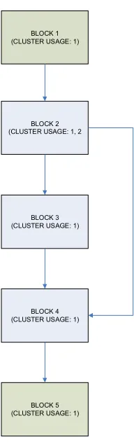
study three-levels of cluster scalability: function-level, treegion-level and basic-block level.
Shutting-off and turning-on the clusters are both done using a “shutoff” instruction. The first
cluster must remain turned-on the whole time since it holds the stack, frame and return
address information.
Figure 3-1 illustrates the format of the shutoff instruction. The immediate field of this
instruction is a bit-vector that indicates which cluster has to be shutoff. For example, “shutoff
1111b” implies that cluster 1, 2, 3 and 4 must be shutoff, and the rest of the clusters (if
Figure 3-1: Shutoff Instruction Format
The “shutoff” instruction has to be the first instruction of the bundle and must be put in
an empty bundle, that is, the rest of the instructions in the bundle must be NOP. This
instruction is decoded by the fetch unit and the appropriate clusters are clock-gated. The rest
of the bundle is ignored and the next bundle is fetched.
3.2 Pipeline Clock-Gating
In CLAW, the fetch unit partially decodes every instruction to see if a shutoff
instruction is fetched. If such an instruction is found, it then emits a signal to the clock-gating
unit to indicate that certain clusters need to be turned off (or turned on). In many previous
works, the clock gating is done only in a single stage. In some works such as [118] [97], they
suggest stalling the processor for ‘N’ cycles (where ‘N’ is the pipeline-depth) and issue a
broadcast to all the units. There are two major problems with this scenario. First, if the
number of shutoffs is not kept to a minimum, the processor stalls significant number of
times. Second, sending these broadcasts requires significant number of long wires, which can
potentially increase power.
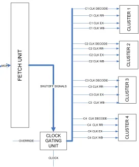
To solve the two problems in the previous work, we created a cascaded clock-gating
circuit. Figure 3-2 shows the high-level block diagram of the clock gating circuit for a
4-cluster CLAW processor. We implemented an override pin just in case the user does not want
simple-gating unit, the propagating unit and the latching unit. The simple-gating unit accepts
the clock as the input and simply calculates whether the clock must be gated or not. Figure
3-3 shows the block-diagram of the simple-gating unit.
F E T C H U N IT C L U S T E R 1 C L U S T E R 2 C LU S T E R 3 C LU S T E R 4 CLOCK GATING UNIT SHUTOFF SIGNALS OVERRIDE CLOCK
C3 CLK RR MOP
C1 CLK EX C1 CLK DECODE
C2 CLK RR
C2 CLK WB
C3 CLK DECODE
C3 CLK WB
C4 CLK WB C4 CLK DECODE
C1 CLK WB
C2 CLK DECODE
C3 CLK EX
C4 CLK RR
C4 CLK EX C2 CLK EX C1 CLK RR
Figure 3-2: Overall Clock Gating Circuit Block Diagram
The propagating unit creates a cascaded clock-signal that is send to the next units. Each
of these clocks has a phase shift of 1 cycle that is fed into each of the stages of the processor.
The latching unit holds the clock gating information given by the fetch unit. This unit ensures
that any external interference does not affect the clock signal. The clock signals can be
changed only by fetch unit with the help of an enable signal. Figure 3-4 shows an example of
cascaded clock output for a 2 Cluster CLAW. At 30ns, the fetch unit is requesting that the
second cluster to be shutoff, and keep the rest of the clusters on. We can see that
“gated_clk_1[1]” shuts off immediately. This is being fed into the decode stage. The rest of
the gated clocks appear to mimic the same behavior as gated_clk_1 but with 1 cycle delay
from its predecessor. At 50ns, ‘0’ was found on the “shutoff_bits” bus, the clock signal did
not change because the enable (shutoff_en) was low.
Figure 3-4: Cascaded CLK Output
The advantage of such a clock-gating circuit is that it doesn’t disrupt any instructions
that are in the pipeline during the previous cycles. Also, there is only one Multi-Op
performance penalty to shutting off clusters. Such techniques have been presented for
a general purpose processor. This complex clock-gating unit only increases the processor
area by 2.1% and did not cause any change in the frequency of the base-processor.
3.3 Next PC Calculation
For doing the appropriate next-PC calculations, we evaluated the different techniques
presented in section 1.1.5. Having a dedicated branch cluster for execution gives the
optimum performance compared to the other two schemes. Having a centralized scheme
seems to be the worst of all three. The branch replication scheme seems to add additional
complexity to the cluster and increase the dynamic code-size, which can have adverse effects
in terms of power consumption.
Some of the disadvantages of having a branch cluster are that the compiler must be
very capable in order to schedule all the branches to one certain cluster. Also, if we chose to
disable a certain number of clusters, the code might not perform as well as expected.
In CLAW ISA, when a jump instruction occurs, the return address register (r9) is
automatically written with address of the next MOP after the jump. On the other hand,
branches do not have any other implicit tasks. This helped us come up with a hybrid scheme
to handle control-transfer instructions. Branches could be executed in any clusters as
necessary. Jumps were all assigned to cluster 1. This mechanism helped reduce the possible
congestion that could happen in branch cluster. At the same time, an explicit instruction is
not necessary to write the return address into the return address register, thus reducing
3.4 Instruction Scheduling and Shutoff Insertion
CLAW is a variable-width processor. The width can be varied with the feedback of the
architect, programmer and the user. In order to do this efficiently, we build such a processor
using a set of two issue clusters. In any clustered system, the biggest bottle-neck is the
inter-cluster communication. In order to reduce this effect, several scheduling algorithms have
been presented by previous researchers. We used the concept of scheduling the instructions
and assigning them in the same cycle called Unified-Assign and Schedule (UAS).
GCC provides several hooks that allow architects to manipulate and intercept the
ready-list at different stages of scheduling [39]. The UAS was attached to the
“TARGET_SCHED_FINISH_GLOBAL” hook. This hook is called immediately after the
treegions are created. Figure 3-5 shows the flow-diagram of the major steps involved in the
UAS implementation. A list of unscheduled RTL is taken from the Treegion scheduler and a
list of instructions that are ready in the current cycle is assembled. GCC does all the
scheduling at the RTL level. Fortunately, almost all RTL can be mapped 1-to-1 with the
CLAW OP in the machine description. Each instruction in this ready list is assigned to a
cluster is picked as per a priority function.
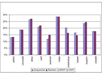
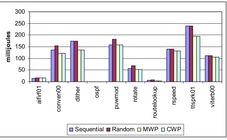
There are four different priority functions available in UAS, they are: sequential
placement, random placement, magnitude-weighted placement (MWP) and
completion-weighted placement (CWP). In sequential placement, the RTLs are assigned in a round-robin
fashion to each cluster. In Random placement, the RTLs are placed to a random cluster
different clusters, either one can be its target. In CWP, the RTL is assigned to the same
cluster as the predecessor that takes the longest to complete. The advantage CWP has over
MWP is that since the current RTL has to wait till the latest of its predecessor to complete,
the holes in between can be used to schedule a copy instruction. These priority functions
have a direct control over the performance and the energy consumption of the processor. We
show the results of all four priority functions in the results section. For more detailed
explanation about UAS, the reader is referred to [34].
LIST OF UNSCHEDULED OPS FROM TREEGION
SCHEDULER
READY LIST == NULL READY_LIST = LIST OF OP
READY IN CURRENT CYCLE
X = HIGHEST PRIORITY OP FROM READY_LIST
PICK APPROPRIATE CLUSTER (C) IN WHICH X
CAN BE SCHEDULED
X SCHEDULABLE IN CLUSTER C ? X = SCHEDULED
INSERT X IN SCHEDULE_LIST WITH APPROPRIATE CLUSTER
INFO
NO
YES
C == NULL
NO
NO INCREMENT CYCLE
COUNT YES
YES
Figure 3-5: Design-Flow of UAS Algorithm on GCC
To make UAS more suitable for a length-adaptive processor, we slightly modified the
assignment-priority function. When an RTL can be assigned to multiple-clusters during
MWP and CWP scheme, the authors in [103] mention to randomly pick a cluster. We forced