by
Rajesh Bollapragada
A thesis submitted to the Graduate Faculty of North Carolina State University
in partial satisfaction of the requirements for the Degree of
Master of Science
Electrical Engineering
Raleigh
2003
Approved By
Dr. Douglas W.Barlage Dr. Rhett Davis
Co-Chair of Advisory Committee Co-Chair of Advisory Committee
Biography
I would like to thank Prof Douglas W. Barlage and Prof Rhett Davis for being on my committee, reviewing my thesis and suggestions. Thanks to all group members, present and past, in EGRC 410 and 412 for making the research work a pleasant learning experience. Finally, I would like to thank my parents and family for making me what I am, today. I do not have enough words to thank them.
Contents
List of Figures vii
1 Introduction 1
1.1 Motivation for and Objective of this Study . . . 2
1.2 Thesis Overview . . . 3
2 Literature Review 4 2.1 Background . . . 4
2.2 Modeling of Quasi-Optical System . . . 5
2.3 Local Reference Terminal . . . 7
2.4 Technology file . . . 8
3 Java Philosophy 11 3.1 Introduction . . . 11
3.2 Event Delegation Model . . . 13
3.3 Class Structure . . . 13
3.4 Summary . . . 14
4 Tool Flow 15 4.1 Introduction . . . 15
4.2 Local Reference . . . 17
4.3 Tool Flow . . . 19
4.3.1 Simulating High Speed Circuits . . . 19
4.3.2 Schematic Capture Flow . . . 22
4.4 EMPDK . . . 24
4.4.1 Introduction . . . 24
4.4.2 Creating a technology file . . . 25
4.5 Electric . . . 26
4.5.1 Introduction . . . 26
5.1.1 Introduction . . . 34
5.1.2 Unit Cell . . . 34
5.1.3 5x5 Grid . . . 35
5.2 Microwave Stub-filter . . . 36
5.2.1 Introduction . . . 36
5.2.2 Simulation Results . . . 37
5.2.3 Performance Measures . . . 42
5.3 Summary . . . 42
6 Conclusion 43 7 Future Research 44 8 Appendix 46 8.1 Appendix A . . . 46
8.1.1 CIF file format . . . 46
8.2 Appendix B . . . 48
8.2.1 EMPDK User Guide . . . 48
8.2.2 Introduction . . . 48
8.2.3 Creating a new technology file . . . 48
8.2.4 Editing an existing technology file . . . 48
8.3 Appendix C . . . 50
8.3.1 Technology File Structure . . . 50
List of Figures
2.1 Planar Grid System. . . 5
2.2 Unit cell with gate bias lines. . . 6
2.3 Equivalent circuit model. . . 6
2.4 A two port micro-strip line. . . 8
2.5 A sample process parameters. . . 9
2.6 Sample technology file. . . 10
3.1 Model-View-Controller architecture. . . 12
4.1 Typical Grid Amplifier System. . . 16
4.2 Division of system in fields and circuits. . . 16
4.3 Unit cell with port voltages and local reference terminals identified. . 17
4.4 Local Reference Groups shown on a 4x4 grid amplifier. . . 18
4.5 Block Diagram of Tool Flow. . . 19
4.6 Preparation of Layout for EM Simulation - Flowchart. . . 21
4.7 Schematic Extraction - Flowchart. . . 23
4.8 EMPDK v1.0 . . . 24
4.9 Sample technology file . . . 25
4.10 Local Reference Terminal. . . 28
4.11 Creating Export. . . 29
4.12 Creating spice netlist. . . 30
4.13 Integrating Electric and EMPDK. . . 31
4.14 Simulation of distributed structures under fREEDA. . . 33
5.1 Unit Cell Dimensions. . . 35
5.2 Unit Cell S21. . . 36
5.3 Microwave stub filter. . . 37
5.4 Stub filter block. . . 38
5.5 Microwave Stubfilter extracted netlist. . . 39
Chapter 1
Introduction
The IC market is characterized by an ever increasing level of integration com-plexity. Today complete systems that previously occupied one or more boards, are integrated on a few chips or even on one single multi–million transistor chip – a so called System– on– Chip (SoC).
Research interest is moving in the direction of system synthesis where an object– oriented system level specification is translated into a hardware–software co-architecture with high level specification for both the hardware, the software and the interfaces. In addition, reuse and platform based design methodologies are being developed to further reduce the design effort for complex systems.
Millimeter-wave circuits are becoming ever more commercially and militarily vi-able and, coupled with large scale production, design practices must evolve to be more sophisticated in order to handle more complex relationship between constituent elements. Also, as the frequency of radio frequency (RF) circuits extends beyond a gigahertz to tens and hundreds of gigahertz, wavelengths become large with respect to device and circuit dimension and the three-dimensional EM environment becomes more significant.
1.1
Motivation for and Objective of this Study
One fundamental issue that arises in modelling electrically large systems in a cir-cuit representation is the assignment of system ground. Currently, circir-cuit simulators use a nodal approach in which voltages are assigned to terminals and each of these voltages is referred to a common reference point, which is commonly called ‘ground’. In a spatially distributed system, a common reference point cannot always be defined as the (electrically significant) spatial separation of a node and its reference point cannot be tolerated. If the separation is an appreciable fraction of a wavelength, it is not possible to uniquely define voltage.
Transmission line effects frequently lead to problems like overshoot, undershoot and ringing. Board interconnects limit performance by introducing delay into the timing path. Crosstalk and EMI are beginning to present formidable problems in what traditionally have been considered acceptable board designs.
EM models, relying on the global reference terminal concept cannot accurately treat large multi-port structures. This thesis presents a tool flow for model develop-ment based on a new concept of local reference nodes (LRN’s). The LRN concept enables the conversion of a port – based model to a terminal- based model, which can be used in a general purpose circuit simulator after modifications to the way the nodal admittance matrix is treated.
the active devices in a non-linear circuit solver. Since the system consists of spatially distributed components, we need a system which can identify the local reference terminals.
This thesis will outline the creation of a tool set with the capability to simu-late spatial power combining systems. This thesis documents the development of a tool flow for integrated steady state nonlinear circuit analysis and electromagnetic analysis of a quasi-optical grid amplifier system. The analysis incorporates surface modes, nonuniform excitation, and full nonlinear effects. The work is verified using measurement of a 5x5 grid amplifier.
1.2
Thesis Overview
This thesis describes the integration of a circuit and field simulator, which will ultimately be used to simulate a grid amplifier.
Chapter 2 is a review of literature relevant to the grid amplifier systems. The review includes modeling of quasi-optical arrays, local reference terminal concept for simulating spatially distributed circuits and the need for a technology file to describe the process in a multilayered system.
Chapter 3 is an overview of the Java philosophy and explains the programming interface.
Chapter 3 is an overview of the program flow required to complete the simula-tion. The overview includes a discussion about each program used and a detailed description of the interfaces between the programs are presented.
Chapter 4 is a case study on modeling a grid amplifier. A detailed description of the model development process as well as results from the completed model are presented
Literature Review
2.1
Background
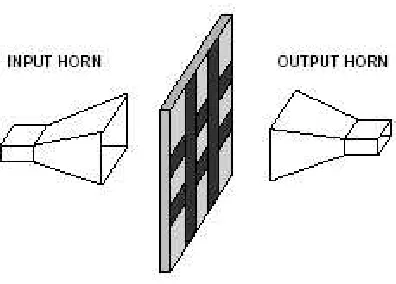
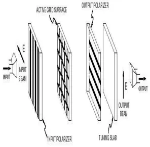
Quasi-optical power combining techniques are a means of combing the power out-put of numerous solid state devices generally in a free space environment. In [6] a review of the various techniques and systems is presented. Mink [3] conducted a theoretical investigation of an array of filamentary current sources radiating into a plano-concave open resonator. Mink [3] discuses the possibility of obtaining high combining efficiency for systems several wavelengths in dimension. The field was fur-ther advanced by the construction of a grid oscillator [4] and grid amplifier [5]. A diagram of the general system is shown in Fig.2.1 The systems represented a proof of concept.
Figure 2.1: Planar Grid System.
from the model. The literature review discusses modeling techniques for quasi-optical grid amplifiers and oscillators.
The power combining system is a way of efficiently coupling the energy via free space instead of using transmission lines. If you use transmission lines, there is an inherent upper limit on the number of elements that can be combined. It finds application in X-band (8 Ghz) and Ka - band (34Ghz) combiners.
2.2
Modeling of Quasi-Optical System
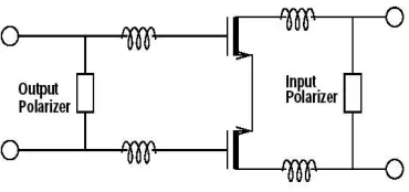
The grid oscillator presented in [4] was one of the early demonstrations of quasi-optical power combining. The system was designed using a unit cell model that is presented in [9]. In [5] Kim presents a grid amplifier.The equivalent circuit and unit cell layout are shown in Fig.2.2 and Fig. 2.3.
In [9] the unit cell model was extended to improve its performance. The surface current distribution was approximated using the method of moments technique and the EMF method was used to calculate the impedance of the grid leads. The sub-strates and free space regions in the systems are represented by transmission lines. The polarizers are modeled by reactive elements.
Figure 2.2: Unit cell with gate bias lines.
of Moments simulator [9] which no longer relied on the unit cell approximation in characterizing planar grid structures. The significance of this work is that surface waves, nonuniform excitation, and gain and phase variations of the unit amplifiers can be considered. Finite grids can now be rigorously specified, with the effects of mutual coupling between cells and variations in magnitude and phase of the feed sources included. The simulator also included the effects of quasi-optical components far away from the grid, such as lenses. The simulator computed an impedance ma-trix for the grid structure, which can be used in a microwave circuit simulator. An implementation is presented in [10]. The gain of an amplifier grid and an analysis of frequency and phase synchronization in oscillator arrays are presented.
2.3
Local Reference Terminal
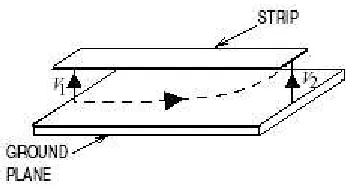
Circuit theory has evolved to include a common reference terminal to which all voltages in a circuit are referred. However, it is generally not feasible to define voltages or a single reference point in a spatially distributed system. In [1] , Steer describes a framework to simulate distributed strucutres. Microstrip networks are examples of distributed structures for which reasonable approximations have been made so that they can be treated as elements in conventional circuit simulators. A micro-strip transmission-line segment is shown in Fig. 2.2 with the conventionally accepted defi-nition shown for the node voltages at the ends of the line. In the common approach, the voltages V1 and V2 are determined as the integral of the electric field from the
strip to the ground plane using the shortest path - defined with vertical arrows. How-ever, an absurd ‘value’ for V2 would be obtained if the integral were to be performed
Figure 2.4: A two port micro-strip line.
2.4
Technology file
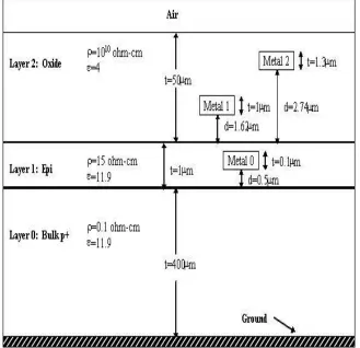
In multi-layered structures, we need to define the layers that are used in the sys-tem. The technology file contains process specific parameters such as layer thicknesses and the sheet resistance of the various layers. In addition to this it also provides the mesher tool with information regarding the ordering of layers. A generic CMOS pro-cess is shown in Figure 2.5. In Figure 2.6 a sample technology file for the given propro-cess is shown.
In conventional layout tools, the technology file contains information pertaining to lambda–based design rules. They do not store the material properties (dielectric constant), (loss tangent), (sheet resistivity), (conductivity), which are essential in characterizing multi-layered structures. The main advantage to having this informa-tion external is that, we can change our process parameters without having to redo our layout.
In addition to this, the information pertaining to the order of layers is also embed-ded in the file. This helps us render a two-dimensional layout to a three-dimensional layout.
// TECHNOLOGY FILE
// METAL LAYERS : 2 // DIELECTRIC LAYERS: 1 technology cmos
UNITS microns metal
//name zmin thickness resistivity(ohms.cm) desc layer 0 0.00 0.35 0.2 // G substrate layer 1 0.7 0.2 1.56E-4 // M
endmetal dielectric
//name zmin thickness dielectric constant layer 2 0.35 0.35 3.9
enddielectric endtechnology
Chapter 3
Java Philosophy
3.1
Introduction
Java is a system-independent object oriented programming language. The pro-gram architecture is based on the MVC (Model–View –Controller architecture). The goal of the MVC design pattern shown in Figure 3.1 is to separate the application object (model) from the way it is represented to the user (view) from the way in which the user controls it (controller).
The model object knows about all the data that need to be displayed. It also knows about all the operations that can be applied to transform that object. However, it knows nothing whatever about the GUI, the manner in which the data are to be displayed, nor the GUI actions that are used to manipulate the data. The data are accessed and manipulated through methods that are independent of the GUI. A simple example of a model would be a clock object. It has intrinsic behaviour whereby it keeps track of time by updating an internal record of the time ever second. The object would provide methods which allow view objects to query the current time. It would also provide methods to allow a controller object to set the current time.
obtain data from the model and then displays the information. The display can take any form, in the clock example, one view object could display the time as an analogue clock, another could show it as a digital clock. The different displays would have no bearing whatsoever on the intrinsic behavior of the clock.
The controller object knows about the physical means by which users manipulate data within the model. In a GUI for example, the controller object would receive mouse clicks or keyboard input which it would translate into the manipulator method which the model understands. For example, the clock could be reset directly by typing the current time into the digital clock display. The controller object associated with the view would know that a new time had been entered and would call the relevant ‘SetTime’ method for the model object.
3.2
Event Delegation Model
The delegation event model supports a clean separation between the core program and its use interface. The delegation pattern allows robust event handling that is less error prone due to strong compile- time checking.
The delegation model consists of three separate objects to deal with event han-dling: event sources, events, and listeners. Event sources are any of the user interface components such as buttons, text fields. Event sources generate and fire events, and the events propagate until they are finally attended to by their listeners.
3.3
Class Structure
Model ClassThe model class is CIF file parser and the Technology file generator.
View Class The view class is composed of the different panels (ex. metalPanel, dielectricPanel, viaPanel, mainMenu)
Chapter 4
Tool Flow
4.1
Introduction
Figure 4.1 is a typical spatial power combining system. The system contains horns for input and output and components which are spread over several wavelengths. The active surface contains numerous nonlinear devices connected to input and output radiators.
The system presents some very challenging problems: components are spatially distributed, power is radiated through the system, and nonlinear devices are present in the system. The first two problems dictate that electromagnetic models be used, however the nonlinear devices are naturally handled in a circuit simulator. The solution is to divide the two problems up as shown in Figure 4.2 .
Figure 4.1: Typical Grid Amplifier System.
4.2
Local Reference
Once the division of the system is done, we need to identify the local reference terminals and the local reference groups. The port–based admittance matrix is nodal in nature as illustrated in Figure 4.3. The local reference terminals are marked as there is no global ground. The implementation of the local reference terminal is discussed in more detail in [2].
V V
V
V4P
P
P
P
1 2
3
LOCAL REFERENCE
Locally Referenced Group
4.3
Tool Flow
Figure 4.5 shows the complete block diagram of the simulation environment which is capable of handling the distributed effects in high speed circuits. Off the shelf tools were taken and modified to capture the distributed effects. The main contribution to the tool flow was adding support to capture the geometrical and electrical properties of a layout and handling the interface between the programs.
EMPDK ELECTRIC G2M SP2IBIS MESHER DC2LIGHT PRIME FREEDA
Figure 4.5: Block Diagram of Tool Flow.
4.3.1
Simulating High Speed Circuits
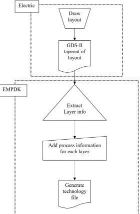
Figure 4.6 shows the steps involved in preparing a generic layout for EM sim-ulation. The system under observation is drawn using Electric. The geometrical information is automatically taped out as a GDS-II file. The additional information included in the GDS-II file is the local reference terminals that are manually identified by the user.
Draw layout
GDS-II tapeout of
layout
Extract Layer info
Add process information for each layer
Generate technology
file EMPDK
Electric
Netlist
Add output statements and
analysis type
Simulate using fREEDA
Draw Schematic Electric
Figure 4.8: EMPDK v1.0
EM-Physical Design Kit is a Java program which takes generic GDS-II or CIF file as its input and produces an output CIF file and an associated technology file. This progam was developed as part of the work for this thesis. It provides an interface between the layout tool and full-wave electromagetics simulator.
The technology file gives us information regarding
• the ordering of the layers, which helps us render the layout to a three–dimensional view.
• provides thickness information of each layer.
The geometrical information of the on-chip placement is obtained from the CIF file. The technology file gives the mapping between the different layers in the CIF file and the generic layers that any layout tool can interpret. The output of EMPDK is a human readable text file.
4.4.2
Creating a technology file
// TECHNOLOGY FILE
// METAL LAYERS : 2 // DIELECTRIC LAYERS: 1
technology cmos UNITS microns metal
//name zmin thickness resistivity(ohms.cm) desc layer 0 0.00 0.35 0.2 // G substrate layer 1 0.7 0.2 1.56E-4 // M
endmetal
dielectric
//name zmin thickness dielectric constant layer 2 0.35 0.35 3.9
enddielectric endtechnology
Figure 4.9: Sample technology file
will be defined in non-conducting oxide layers. The sheet resistance of the metal layers is specified in milli-Ohms/Square along with the metal thickness. The z-coordinate of the bottom of the metal layer is specified under zmin where zmin is the distance in microns from the bottom of the substrate layer to the bottom of the metal layer.
You can also define optional vias to make connections from metal layer to metal layer. Note that vias are totally optional and usually play a minor role in determining the characteristics of a device. On the other hand, one can create multi-layer devices, or symmetric center-tapped inductors, with many via connections in series with the device. In these situations the inclusion of vias is necessary. Via layers are added in the ‘via’ sections. The top and bottom sections define the metal connectivity of the via. Note that the numbers correspond to the numbers used in the ‘metal’ sections.
4.5
Electric
4.5.1
Introduction
The Electric VLSI Design System is a highly flexible and powerful system that can handle many different types of circuit design (MOS, Bipolar, schematics, printed circuitry, hardware description languages, etc.) It handles geometry at any angle (not just Manhattan) and can even handle curves.
can aid in design to an unprecedented degree. Electric maintains circuit information based on connectivity. This feature was made us to incorporate the idea of local reference terminal in Electric.
Electric has many analysis tools, including design-rule checking, simulation, and network comparison. Electric has many synthesis tools, including routing, com-paction, silicon compilation, PLA generation, and compensation,
The user interface is quite sophisticated and runs on all popular workstations (Windows, Macintosh, and UNIX). It also provides interpretive languages (Lisp, TCL, and Java) for advanced users.
The most interesting feature of the system is its global enforcement of connectivity which provides top-down design capability and ease of post-design modifications. The features provided by Electric is described in the progammers reference manual [7].
In the next few sections we will see how a layout is prepared for either EM simu-lation or in general the process for going from layout to circuit netlist simusimu-lation.
4.5.2
Identifying the Local Reference
A facet as shown in Figure 4.10 can represents a local reference group or a system of local reference groups. Electric is based on the connectivity approach, it stores terminal information for the given schematic. This information is used to identify the reference terminals on a facet.
The tool was modified to automatically identify the local reference terminal. This information is available to the user as a extension to the CIF file of the layout.
4.5.3
Creating Exports in a Schematic
data, we can generate a netlist describing the electrical circuit as shown in Figure 4.12.
4.6
Integrating Electric and EMPDK
In addition to the netlist we also output two files, which make the system an EM-Aware system. These files describe the geometry of the distributed structures in the layout and also provide process parameters of the layers used to layout the circuit.
Layout Extraction Mixed Layout Electric EM-Aware Technology file Parasitic Extractor FREEDA
Figure 4.13: Integrating Electric and EMPDK.
The integration of Electric and EMPDK is shown in Figure 4.13.The above infor-mation is given as input to fREEDA to extract the port voltages in the circuit.
4.7
fREEDA
4.7.1
Introduction.
fREEDA(TM) is a multi-physics circuit simulator under development by a user community from universities, communities and laboratories.
tion methods available), harmonic balance analysis and a unique wavelet transient analysis.
It also implements various linear devices from resistors to Foster’s canonical port representation and non-linear devices from diodes to three and four terminal transis-tors.
4.7.2
Simulating structures
Case Study
5.1
Quasi Grid Amplifier
5.1.1
Introduction
The earlier chapters described the approach towards an integrated design environ-ment for design of spatial power combining systems. In this chapter various results are presented. The achievement is that the same results are obtained with the current design environment compared to previous results in [10].
In this section various size grids are analyzed and the intermediate CIF data is compared with that in [10]. The principle achievement is that the CIF output generated automatically by this work is exactly same to that handgenerated by user in [10]. This indicates that the CIF output precisely captures the geometry.
5.1.2
Unit Cell
Figure 5.1: Unit Cell Dimensions.
results obtained by simulation and the dashed line is for the measurements taken. In Fig. 5.1 , the geometry for a unit cell of dimension 93.8 mm x 93.8 mm with a gap spacing of 9.8 mm and a line width of 6.35 mm is shown.
5.1.3
5x5 Grid
1.8 2 2.2
0
FREQUENCY (GHz)
1 2 3 4 5 6 7 8
Figure 5.2: Unit Cell S21.
5.2
Microwave Stub-filter
5.2.1
Introduction
Figure 5.2 is a microwave stub filter. A microwave filter is a two port network used to control the frequency response at a certain point in a microwave system by providing transmission at frequencies within the passband of the filter and attenuation in the stopband of the filter. Typical frequency response include low-pass, high-pass, band-pass and band-reject characteristics. Applications can be found in virtually any type of microwave communication, radar, or test and measurement system.
Port
1 Port 2
23 mm 92 mm 92 mm 18.4 mm 4.6 mm 4.6 mm
Figure 5.3: Microwave stub filter.
Both these methods provide lumped element circuits. For microwave applica-tions, such designs usually must be modified to use distributed elements consisting of transmission line sections. The Richard’s transformation and the Kuroda identities provide this step.
Figure 5.3 describes the process or the layers that makeup the stub filter.
5.2.2
Simulation Results
In this particular case–study, we were able to successfully identify distributed structures in a layout as opposed to considering then as simple wires. The individual components in the netlist we correctly identified. The user had to manually enter the analysis type required. Figure 5.4 shows the extracted netlist of the microwave stubfilter under inspection.
Figure 5.4: Stub filter block.
*transim netlist
vsource:v1 1 0 vac = 1 .ref 5
tlinp4:t1 21 0 2 0
+ z0mag=75.00 length=5e-3 k=7 tand=.01 fscale=1.e10 alpha=1.
+ nsect = 20 fopt=35e9
tlinp4:t2 2 3 4 5
+ z0mag=38.53 length=18e-3 k=7 tand=.01 fscale=1.e10 alpha=1.
+ nsect = 20 fopt=35e9
tlinp4:t3 3 0 6 0
+ z0mag=75.00 length=10e-3 k=7 tand=.01 fscale=1.e10 alpha=1.
+ nsect = 20 fopt=35e9
res:rl 6 32 r=75 vsource:v2 32 0 res:r2 1 21 r=75 res:ropen 4 5 r=10K
.ac start = 4.5e9 stop = 8e9 n_freqs = 100
.out plot element "vsource:v2" 0 if mag db in "atten.out" .out plot element "vsource:v1" 0 if in "input.out"
.end
11
S
1.5 2 2.5 3 3.5 4
Frequency (GHz)
(dB)
-10
-12 -8 -6 -4 -2 0
1
21
(dB)
S
1.5 2 2.5 3 3.5 4
Frequency (GHz) 0
-5
-10
-15
-20
-25
-30
-35
-40
-451
• Since all the tools are GPL licensed software, allows programmability/customizability and seamless integration.
• Can be used with additional libraries like MPI(parallel algorithm) to improve efficiency
Accuracy of the simulated results
It has been shown that the automatically generated CIF file matches with the hand generated, published by Patwardhan[10]. With the incorporation of the local reference groups, we make sure that effects like time delay, substrate coupling are simulated accurately. The current distribution values and the s-parameters extracted from the full-wave simulator for simple structures were in agreement with the measured data.
5.3
Summary
Chapter 6
Conclusion
Future Research
Appendix
8.1
Appendix A
8.1.1
CIF file format
Caltech Intermediate Format (CIF) is a recent form for the description of inte-grated circuits. Created by the university community, CIF has provided a common database structure for the integration of many research tools. CIF provides a limited set of graphics primitives that are useful for describing the two-dimensional shapes on the different layers of a chip. The format allows hierarchical description, which makes the representation concise. In addition, it is a terse but human-readable text format. CIF is therefore a concise and powerful descriptive form for VLSI geometry. Each statement in CIF consists of a keyword or letter followed by parameters and terminated with a semicolon. Spaces must separate the parameters but there are no restrictions on the number of statements per line or of the particular columns of any field. Comments can be inserted anywhere by enclosing them in parenthesis.
BOX to draw a rectangle, WIRE to draw a path, ROUNDFLASH to draw a circle, POLYGON to draw an arbitrary figure, and CALL to draw a subroutine of other geometry statements. The control statements are DS to start the definition of a subroutine, DF to finish the definition of a subroutine, DD to delete the definition of subroutines, 0 through 9 to include additional user-specified information, and END to terminate a CIF file. All of these keywords are usually abbreviated to one or two letters that are unique.
Label Command
94 Input 10,20 Type”Input” Reference=”Ground”;
This command is another common extension and is used to mark points with a name. The parameters are the name of the label, and the x and y coordinates of the point.
Extensions to CIF can be done with the numeric statements 0 through 9. Al-though not officially part of CIF, certain conventions have evolved for the use of these extensions
Sample CIF File
This is a sample CIF file modeling a dipole antenna. The units are in millimeters. The name of the layout is ‘dipole’. It consists of two boxes on a metal1 type layer.
The centers of two cells are located at the coordinates (-100; 0) and (100; 0), and both cell sizes are 200 mm x 200 mm (square boxes). A circuit port (See chapter 3 for port description) is specified at the coordinate (0; 0).
DS 1 1 1; 9 Dipole; L metal1;
B 200 200 -100,0; B 200 200 100,0;
94 Ground 0,0 Type=”Ground”; DF;
are the material properties of the layers in the layout. The output of EMPDK is in a human–readable form. This file can be imported to other layout tools like Cadence, LinkCad etc.
8.2.3
Creating a new technology file
The user must have information regarding the process and the layers that go into the layout. To create a new file, the user has to select the option ‘New’ from the ‘File’ Menu.
After providing the ‘filename’ the user will be prompted for information regarding the layers in the process. This information has be entered starting with the substrate layer working your way upwards.
Once the user is done entering the information for each of the layers in the process, he/she can select the ‘Done’ button in the dialog box. This will automatically generate the file for the user.
More information regarding the layer types supported and how to specify dimen-sions are given in Appendix C.
8.2.4
Editing an existing technology file
// DIELECTRIC LAYERS: 1
technology cmos UNITS microns metal
//name zmin thickness resistivity(ohms.cm) desc layer 0 0.00 0.35 0.2 // G substrate layer 1 0.7 0.2 1.56E-4 // M
endmetal
dielectric
//name zmin thickness dielectric constant layer 2 0.35 0.35 3.9
enddielectric endtechnology
Figure 8.1: Sample technology file
The technology file allows the user to specify the process related parameters. The characteristic information obtained from the technology is used
• to specify the thickness of the layers
• obtain the ordering of the layers
• to obtain the electrical parameters like resistivity, dielectric constant, etc.
[1] Steer, Harvey, Mink, Abdulla, Christofferson, Gutierrez, Heron, Hicks, Khalil, Mughal, Nakazawa, Nuteson, Patwardhan, Skaggs, Summers, Wang and Yakovlev. “Global Modeling of Spatially Distributed Microwave and Millimeter-Wave Systems,”IEEE Transactions on Microwave Theory and Techniques, June 1999, Vol. 47, No. 6.
[2] Steer, Christofferson. “Implementation of local reference node concept for spa-tially distributed circuit,” Int J. on RF and Microwave Computer Aided Engi-neering, Sept. 1999, Vol. 9, No. 5.
[3] Mink. “Quasi-optical power combining of solid-state millimeter-wave sources,” IEEE Trans. Microwave Theory Tech., Vol. 34, pp. 273–279, Feb. 1986.
[4] Popovic, Kim, and Rutledge “A grid oscillators,”. Int. Journal Infrared and Mil-limeter Waves., Vol. 9, pp. 1003–1010, Nov. 1988.
[5] Kim, Rosenberg, Smith, Weikle, Hacker, De Lisio, and Rutledge. “A grid ampli-fier,”. IEEE Microwave Guided Wave Lett., Vol. 1, pp. 322–324, Nov. 1991.
[6] York. “Quasi-optical power combining techniques,” SPIE Critical Reviews of Emerging Technologies, 1994.
[7] Steven Rubin. “Computer Aids for VLSI Design,”. www.staticfreesoft.com
[9] Nuteson. Electromagnetic Modeling of Quasi-Optical Power Combiners Ph.D Dissertation, NC State, 1997.
[10] Patwardhan. Modular Computer Aided Field Modeling of Spatial Power Com-bining System MS Thesis, NC State, 1997.
[11] Uppathil. Layout Oriented Design Practice for Capturing Distributed Effects in High Speed Circuit Design MS Thesis, NC State, 2002.
[12] Pozar.Microwave Engineering John Wiley & Sons, Second Edition, 1997.