Enhancement of the Power Quality and
Reliability by Using Dual Voltage Source
Inverter (DVSI) of the Microgrid System
Chilla Nagaratnamma1, G.Subbarao Guptha 2, K. Purushotham3
M.Tech Student, Dept of EEE, Ananthalakshmi Institute of Technology & Sciences, Affiliated to JNTUA, A.P, India1. Assistant Professor, Dept of EEE, Ananthalakshmi Institute of Technology & Sciences, Affiliated to JNTUA,
A.P, India. 2
Assistant Professor, Dept of EEE, Ananthalakshmi Institute of Technology & Sciences, Affiliated to JNTUA , A.P, India3
ABSTRACT: The paper focuses on a Dual-commutated voltage source Inverter (DVSI) connected to a grid in a wind
energy application. The proposed scheme is involved two inverters, which empowers the micro grid to trade power created by the distributed energy resources (DERs) furthermore to compensate the nearby unbalanced and nonlinear burden. The control calculations are produced taking into account instantaneous symmetrical component theory (ISCT) to work DVSI in grid sharing and grid infusing modes. The proposed plan has expanded unwavering quality, lower data transfer capacity necessity of the primary inverter, lower taken a toll because of diminishment in channel size, and better use of micro grid power while utilizing lessened dc-link voltage rating for the fundamental inverter.
I. INTRODUCTION
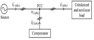
The renewable energy sources are integrated to the network with Distributed Generation(DG). These DG units with co-ordinate control of local generation and storage facilities form a microgrid. In microgrid, power from various renewable sources are interfaced with grid and loads using power electronic converters. A microgrid inverter is used to exchange the power from microgrid to the grid and connected load. This microgrid inverter can be operated in grid sharing mode for supplying a part of local load, and in grid injecting mode for injecting power to main grid. In general the unbalanced load causes low voltage on one leg, power delivery problems and resistance breakdown problems inside the motor or system.If there is a considerable amount of feeder impedance in the distribution systems, the propagation of the harmonic currents distorts the voltage at the point of common coupling (PCC). Industry automation has reached to a very high level of comfortable, plants like auto mobiles manufacturing units, chemical factories, and semiconductor industries required accurate power. The microgrid inverter is used foractive power injection as well as for load compensation; the inverter capacity that can be used for fulfilling the second task is decided by the available instantaneous microgrid real power.
power is supplied by two inverters, power losses across the semiconductor switches of each inverter are reduced. This increases its reliability as compared to a single inverter with multifunctional capabilities. Also, smaller size modular inverters can operate at high switching frequencies with a reduced size of interfacing inductor, the filter cost gets reduced. The inverters in the proposed scheme use two separate dc links. Since the auxiliary inverter is supplying zero sequence of load current, a three-phase three-leg inverter topology with a single dc storage capacitor can be used for the main inverter. This in turn reduces the dc-link voltage requirement of the main inverter. Thus, the use of two separate inverters in the proposed DVSI scheme provides increased reliability, better utilization of microgrid power, reduced dc grid voltage rating, less bandwidth requirement of the main inverter, and reduced filter size. Control algorithms are developed by instantaneous symmetrical component theory (ISCT) to operate DVSI in grid-connected mode, while considering nonstiff grid voltage. The extraction of fundamental positive sequence of PCC voltage is done by dq0 transformation.
II. EXISTING METHOD
The existing method describes the power quality is an important aspect which has to be addressed while the micro- grid system is connected to the main grid Load compensation and power injection using grid interactive inverters in microgrid have been presented in the literature single inverter system with power quality enhancement is discussed. The main focus of this work is to realize dual functionalities in an inverter that would provide the active power injection from a solar PV system and also works as an active power filter, compensating unbalances and the reactive power required by other loads connected to the system.
III. PROPOSED METHOD
The proposed method describes a voltage regulation and power flow control scheme for a wind energy system (WES) is proposed. A distribution static compensator (DSTATCOM) is utilized for voltage regulation and also for active power injection. The control scheme maintains the power balance at the grid terminal during the wind variations using sliding mode control This paper demonstrates a dual voltage source inverter (DVSI) scheme, in which the power generated by the microgrid is injected as real power by the main voltage source inverter (MVSI) and the reactive, harmonic, and unbalanced load compensation is performed by auxiliary voltage source inverter (AVSI).
IV. DUAL VOLTAGE SOURCE INVERTER
A. System Topology
This paper exhibits a double voltage source inverter (DVSI) plan, in which the power produced by the micro grid is infused as genuine Power by the fundamental voltage source inverter (MVSI) and the reactive, harmonic, and unbalanced load pay
is performed by helper voltage source inverter (AVSI). This has favorable position that the evaluated limit of MVSI can simply be utilized to infuse genuine energy to the system, if adequate renewable Power is accessible at the dc link. In the DVSI plan, as total load power is supplied by two inverters, power losses over the semiconductor switches of every inverter are lessened. This expands its unwavering quality when contrasted with a solitary inverter with multifunctional abilities. Additionally, littler size secluded inverters can work at high exchanging frequencies with a decreased size of interfacing inductor, the channel cost gets decreased. In addition, as the principle inverter is supplying real power, the inverter needs to track the basic positive arrangement of current. This decreases the data transfer capacity necessity of the principle inverter.
high-frequency switching parts created due to the switching of power electronic switches in the inverters. The system considered in this study is accepted to have some measure of feeder resistance Rg and inductance Lg. Due to the nearness of this feeder impedance, PCC voltage is influenced with sounds.
Fig. 1. Topology of proposed DVSI scheme. Strategy for the reference current generation of two inverters in DVSI scheme.
B. Design of DVSI Parameters
1) AVSI: The vital parameters of AVSI like dc-connection voltage (Vdc), dc storage capacitors (C1 and C2), interfacing inductance (Lfx), and hysteresis band (±hx) are chosen based on the outline technique for split capacitor DSTATCOM topology. The dc-link voltage over every capacitor is taken as 1.6 times the top of stage voltage. The total dc-link voltage Reference (Vdcref) is observed to be 1040 V.
Estimations of dc capacitors of AVSI are picked taking into account the change in dc-link voltage during transients. Let complete load rating is S kVA. In the most pessimistic scenario, the load power may shift from least to most extreme, i.e., from 0 to S kVA. AVSI needs to trade real power during transient to keep up the load power request. This transfer of real power during the transient will bring about deviation of capacitor voltage from its reference value. Accept that the voltage controller takes n cycles, i.e., nT seconds to act, where T is the system day and age. Consequently, most extreme energy trade by AVSI during transient will be nST. This energy will be equivalent to change in the capacitor put away energy. Accordingly
Where Vdcr and Vdc1 are the reference dc voltage and maximum permissible dc voltage across C1 during transient, respectively. Here, S =5 kVA, Vdcr = 520 V, Vdc1 = 0.8 Vdcr or 1.2 Vdcr, n = 1, and T = 0.02 s. Substituting these values in (1), the dc link capacitance (C1) is calculated to be 2000 μF. Same value of capacitance is selected for C2. The interfacing inductance is given by
C. Advantages of the DVSI Scheme
The different preferences of the proposed DVSI plan over a single inverter plan with multifunctional capacities are examined here as takes after:
1)Increased Reliability: DVSI plan has expanded dependability, because of the decrease in disappointment rate of
comes up short, the other can proceed with its operation. This decreases the lost energy and subsequently the down time cost. The lessening in system down time cost enhances the unwavering quality.
2)Reduction in Filter Size: In DVSI plan, the current supplied by every inverter is decreased and thus the present
rating of individual channel inductor decreases. This decrease in current rating decreases the channel size. Additionally, in this plan, hysteresis current control is utilized to track the inverter reference currents. As given in (2), the channel inductance is chosen by the inverter switching frequency. Since the lower current evaluated semiconductor device can be exchanged at higher switching frequency, the inductance of the channel can be brought down. This decrease in inductance further diminishes the channel size.
3)Improved Flexibility: Both the inverters are nourished from separate dc links which permit them to work freely,
consequently expanding the adaptability of the system. Case in point, if the dc connection of the principle inverter is detached from the system, the load pay ability of the assistant inverter can in any case be used.
4)Better Utilization of Micro grid Power: DVSI plan uses full limit of MVSI to exchange the whole power produced
by DG units as real power to ac bus, as there is AVSI for symphonious and responsive Power remuneration. This builds the active power infusion ability of DGs in micro grid.
5) Reduced DC-Link Voltage Rating: Since, MVSI is most certainly not conveying zero succession load current
parts; a solitary capacitor three-leg VSI topology can be utilized. In this way, the dc link voltage rating of MVSI is decreased around by 38%, when contrasted with a single inverter system with split capacitor VSI topology.
V. CONTROL STRATEGY FOR DVSI SCHEME
A. Fundamental Voltage Extraction
The control calculation for reference current generation using ISCT requires adjusted sinusoidal PCC voltages. As a result of the nearness of feeder impedance, PCC voltages are misshaped. In this manner, the key positive grouping segments of the PCC voltages are separated for the reference current generation. To change over the mutilated PCC voltages to balanced
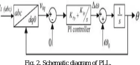
Fig. 2. Schematic diagram of PLL.
Where
So as to get θ, an altered synchronous reference outline (SRF) phase locked loop (PLL) is utilized. The schematic
outline of this PLL is appeared in Fig. 2. It for the most part comprises of a proportional integral (PI) controller and an integrator. In this PLL, the SRF terminal voltage in q-pivot (vtq) is contrasted and 0 V what's more, the mistake voltage
in this way got is given to the PI controller. The recurrence deviation Δω is then added to the reference recurrence ω0
lastly given to the integrator to get θ. It can be demonstrated that, when, θ = ω0 t and by utilizing the Park's change
system(C), q-pivot voltage in dq0 outline gets to be zero and thus the PLL will be bolted to the reference frequency
(ω0). As PCC voltages are mutilated, the changed voltages in dq0 outline (vtd and vtq) contain normal and wavering
segments of voltages. These can be spoken to as
Where vtd and vtq speak to the normal segments of vtd and vtq, separately. The terms and show the swaying segments of vtd and vtq, separately. Presently the principal positive sequence of PCC voltages in normal reference frame can be acquired with the assistance of opposite dq0 change as given by
These voltages v+ ta1, v+ tb1, and v+ tc1 are utilized as a part of the reference current generation calculations, in order to draw adjusted sinusoidal currents from the grid.
B. Instantaneous Symmetrical Component Theory
ISCT was produced basically for unbalanced and nonlinear load pay by active power filters. The system topology appeared in Fig. 3 is utilized for understanding the reference current for the compensator. The ISCT for load compensation is inferred in light of the accompanying three conditions.
1) The source neutral current must be zero. Therefore
2) The phase angle between the fundamental positive sequence voltage (v+ ta1) and source current (isa) is φ
3) The average real power of the load (Pl) should be supplied by the source
Solving the above three equations, the reference source currents can be obtained as
Where the term φ is the desired phase angle between the fundamental positive sequence of PCC voltage and source current. To achieve unity power factor for source current, substitute β = 0in (9). Thus, the reference source currents for three phases are given by
Where i∗ sa, i∗ sb, and i∗ sc are principal positive succession of load streams drawn from the source, when it is supplying a normal load power Pl. The Power Pl can be processed utilizing a moving normal channel with a window of one-cycle information focuses as given below
Where t1 is any arbitrary time instant. Finally, the reference currents for the compensator can be generated as follows:
C. Control Strategy of DVSI
Control system of DVSI is produced in a manner that grid and MVSI together share the active load power, and AVSI supplies rest of the power segments requested by the load.
1) Reference Current Generation for Auxiliary Inverter:
The dc-link voltage of the AVSI ought to be looked after steady for appropriate operation of the helper inverter. DC-link voltage variety happens in helper inverter because of its switching and ohmic losses. These losses termed as Ploss ought to likewise be supplied by the lattice. An expression for Ploss is inferred on the condition that normal dc capacitor current is zero to keep up a steady capacitor voltage. The deviation of normal capacitor current from zero will reflect as an adjustment in capacitor voltage from a steady state value. A PI controller is utilized to produce Ploss term as given by
Where evdc = Vdcref − vdc, vdc speaks to the genuine voltage detected and upgraded once in a cycle. In the above
condition, KPv furthermore, KIv speak to the relative and vital increases of dc-connection PI controller, separately. The Ploss expression hence got ought to be supplied by the lattice, and hence AVSI reference currents can be gotten as given in (14). Here, the dc-link voltage PI controller additions are chosen in order to guarantee soundness and better dynamic reaction during load change.
2) Reference Current Generation for Main Inverter:
The MVSI supplies adjusted sinusoidal currents in view of the available renewable power at DER. On the off chance that MVSI misfortunes are dismissed, the Power infused to framework will be equivalent to that accessible at DER
(Pμg). The accompanying condition, which is gotten from ISCT can be utilized to produce MVSI reference currents for
three phases (a, b, and c)
Fig. 4. Schematic diagram showing the control strategy of proposed DVSI scheme.
Comparator. This controller has the advantage of peak current constraining limit, good dynamic response, and straightforwardness in usage. A hysteresis controller is a high-increase corresponding controller. This controller includes certain phase lag in the operation in view of the hysteresis band and won't make the system temperamental. Likewise, the proposed DVSI plan utilizes a initially arrange inductor channel which retains the closed-loop system strength. The whole control procedure is schematically spoken to in Fig. 4. Applying Kirchhoff’s present law (KCL) at the PCC in Fig. 4
By using (14) and (16), an expression for reference grid current in phase-a can be obtained as
It can be watched that, if the amount (Pl + Ploss) is greater than Pμg, the term [(Pl + Ploss) − Pμg] will be a positive
amount, what's more, i∗ ga will be in stage with v+ ta1. This operation can be called as the system supporting or lattice sharing mode, as the aggregate load power interest is shared between the principle inverter and the system. The term, Ploss is generally little contrasted with Pl. Then again, if (Pl + Ploss) is not exactly Pμg, then [(Pl + Ploss) − Pμg] will
VI. SIMULATION RESULTS
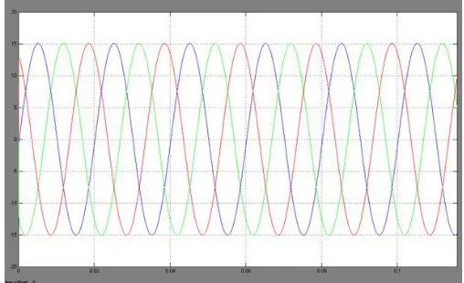
Fig. 5. Without DVSI scheme: (a) PCC voltages
Fig. 5. Without DVSI scheme: (b) fundamental positive sequence of PCC voltages.
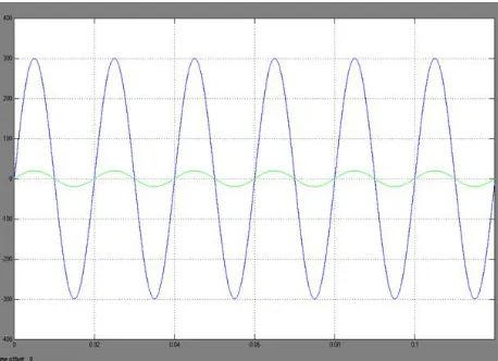
Fig. 6. Active power sharing: (b) active power supplied by grid;
Fig. 6. Active power sharing: (c) active power supplied by MVSI;
Fig. 7. Reactive power sharing: (a) load reactive power
Fig. 7. Reactive power sharing: (b) reactive power supplied by AVSI;
Fig. 8. Simulated performance of DVSI scheme: (a) load currents;
Fig. 8. Simulated performance of DVSI scheme: (b) grid currents;
Fig. 8. Simulated performance of DVSI scheme: (d) AVSI currents.
Fig. 9. Grid sharing and grid injecting modes of operation: (a) PCC voltage and grid current (phase-a).
Fig. 10. DC-link voltage of AVSI
Fig. 11. Proposed PI controller-Gird Current THD =2.81%
EXTENSION RESULTS
VII. CONCLUSION
A DVSI plan is proposed for micro grid systems with upgraded power quality. Control calculations are produced to create reference streams for DVSI utilizing ISCT. The proposed plan has the ability to trade power from disseminated generators (DGs) furthermore to repay the nearby unequal also, nonlinear load. The execution of the proposed plan has been approved through recreation and test thinks about. When contrasted with a single inverter with multifunctional capacities, a DVSI has numerous favorable circumstances, for example, expanded unwavering quality, lower cost because of the decrease in channel size, and more usage of inverter ability to infuse real power from DGs to micro grid. In addition, the utilization of three-phase, three wire topology for the primary inverter lessens the dc-link voltage necessity. Therefore, a DVSI plan is a reasonable interfacing alternative for micro grid supplying sensitive loads.
REFERENCES
[1] A. Kahrobaeian and Y.-R. Mohamed, “Interactive distributed generation interface for flexible micro-grid operation in smart distribution systems,” IEEE Trans. Sustain. Energy, vol. 3, no. 2, pp. 295–305, Apr. 2012.
[2] N. R. Tummuru, M. K. Mishra, and S. Srinivas, “Multifunctional VSC controlled micro grid using instantaneous symmetrical components theory,” IEEE Trans. Sustain. Energy, vol. 5, no. 1, pp. 313–322, Jan. 2014.
[3] Y. Zhang, N. Gatsis, and G. Giannakos, “Robust energy management for micro grids with high-penetration renewable,” IEEE Trans. Sustain. Energy, vol. 4, no. 4, pp. 944–953, Oct. 2013.
[4] R. Majumder, A. Ghosh, G. Ledwich, and F. Zare, “Load sharing and power quality enhanced operation of a distributed micro grid,” IET Renewable Power Gener., vol. 3, no. 2, pp. 109–119, Jun. 2009.
[5] J. Guerrero, P. C. Loh, T.-L. Lee, and M. Chandorkar, “Advanced control architectures for intelligent micro grids—Part II: Power quality, energy storage, and ac/dc micro grids,” IEEE Trans. Ind. Electron., vol. 60, no. 4, pp. 1263–1270, Dec. 2013.
[6]Y. Li, D. Vilathgamuwa, and P. C. Loh, “Microgrid power quality enhancement using a three-phase four-wire grid-interfacing compensator,” IEEE Trans. Ind. Appl., vol. 41, no. 6, pp. 1707–1719, Nov. 2005.
[7] M. Schonardie, R. Coelho, R. Schweitzer, and D. Martins, “Control of the active and reactive power using dq0 transformation in a three-phase grid-connected PV system,” inProc. IEEE Int. Symp. Ind. Electron., May 2012, pp. 264–269.
[8] R. S. Bajpai and R. Gupta, “Voltage and power flow control of grid connected wind generation system using DSTATCOM,” inProc. IEEE Power Energy Soc. Gen. Meeting—Convers. Del. Elect. Energy 21st Century, Jul. 2008, pp. 1–6.
[9] M. Singh, V. Khadkikar, A. Chandra, and R. Varma, “Grid interconnection of renewable energy sources at the distribution level with power-quality improvement features,”IEEE Trans. Power Del., vol. 26, no. 1, pp. 307–315, Jan. 2011.