Together with the fast development of the semiconductor technologies, storage memory technologies had been going through extremely fast changes day-by-day. The volatile and non-volatile memories take up the main part of the contemporary storage memory market shares. Due to the different working states of volatile and non-volatile memories, they are used as main memory and secondary memory respectively. A new storage memory device called double floating gate FET has the potential of functioning as volatile and non-volatile devices simultaneously. It may change the storage memory market by combining volatile and non-volatile devices into one device. In the future, a new storage memory chip functions as volatile and non-volatile devices will replace traditional storage memory chips like DRAM and flash memory.
The working mechanisms of the double floating gate FET is similar to traditional flash memory, so it’s important to control the changings of threshold voltages of this device. Based on previous work of building double floating gate FETs, this thesis focused on building a complete storage memory based on double floating gate FETs. This thesis included a SPICE compatible model of double floating gate FET and a complete peripheral circuit. The performances of desired storage memory composed of double floating gate FETs were tested.
variations.
by Junning Jiang
A thesis submitted to the Graduate Faculty of North Carolina State University
in partial fulfillment of the requirements for the degree of
Master of Science
Electrical Engineering
Raleigh, North Carolina 2015
APPROVED BY:
_______________________________ _______________________________
Dr. Paul D. Franzon Dr. Veena Misra
Committee Chair
DEDICATION
BIOGRAPHY
ACKNOWLEDGMENTS
First of all, I wish to express my gratitude to Dr. Franzon, for this valuable chance into studying the state-of-art devices and circuits. This work contained his time and concentration into the electrical engineering area.
Secondly, I would like to thank Dr. Neil Di Spigna and Dr. Veena Misra. Their approvals of becoming my master’s thesis committee member are important to me. Their experience, suggestions are priceless in this thesis work.
TABLE OF CONTENTS
LIST OF TABLES .………....……….. vii
LIST OF FIGURES ..…..……… viii
CHAPTER 1 INTRODUCTION... 1
1.1 Background and Motivation ... 1
1.2 Thesis Outline ... 3
CHAPTER 2 LITERATURE REVIEW ... 5
2.1 Current Solid-State Semiconductor Memory Technologies ... 5
2.2 Volatile Memories ... 5
2.2.1 DRAM ... 6
2.2.2 SRAM ... 8
2.3 Non-Volatile Memories ... 10
2.3.1 Flash Memory... 11
2.3.2 NOR Flash Memory ... 13
2.3.3 NAND Flash ... 15
2.4 Double Floating Gate ... 16
2.4.1 Volatile Mode ... 18
2.4.2 Non-Volatile Mode ... 19
2.5 Applications and Challenges for Double Floating Gate FET ... 20
CHAPTER 3 SPICE COMPATIBLE MODEL OF FLOATING GATE DEVICES 21 3.1 Computing Algorithms ... 22
3.2 Iteration Steps and Results ... 24
CHAPTER 4 PERIPHERAL CIRCUITS DESIGN AND PERFORMANCE OPTIMIZATION ... 28
4.1 Systematic Diagrams of Double Floating Gate FET Array ... 29
4.2 Row and Column Decoder ... 31
4.3 Internal Clock Source ... 33
4.4 Level Shifters ... 36
4.4.1 Positive Level Shifter ... 37
4.4.2 Negative Level Shifter... 38
4.5 Sense Amplifier ... 42
4.6 Piecewise Linear Write Circuit ... 44
4.6.1 Basic Ideas ... 44
4.6.2 Constant Gm Bias Circuit ... 47
4.6.3 Auxiliary Network in Generating Current ... 48
4.6.4 Piecewise-Write Demonstration ... 49
4.6.5 Increased Read Noise Margin from Piecewise Linear Write Circuit ... 50
4.6.6 Reducing the Micro-Level Variation ... 51
4.7 Controller Design ... 52
CHAPTER 5 DOUBLE FLOATING GATE FET ARRAY OPERATION ... 54
5.1 Operations of Double Floating Gate FET Array ... 55
5.2 Simulation Process and Results ... 56
CHAPTER 6 CONCLUSIONS AND FUTURE WORK ... 57
6.1 Conclusion ... 57
6.2 Future work ... 57
REFERENCES ... 59
APPENDICES ... 61
Appendix A Verilog-A module ... 62
Appendix B VCO ... 77
Appendix C Positive Level Shifter... 81
Appendix D Negative Level Shifter ... 85
Appendix E Constant-gm Bias Network ... 88
Appendix F Auxiliary Network ... 91
Appendix G Double Floating Gate FET Array ... 94
LIST OF TABLES
Table 2-1 Comparison between the Flash memory and Emerging Nonvolatile Memory
Alternatives [1] ... 11
Table 3-1 Descriptions of Four States of Double Floating Gate ... 27
Table 4-1 MOSFET Sizes and Technologies of Two Input Decoder ... 31
Table 4-2 MOSFET Sizes and Technologies of VCO ... 34
Table 4-3 MOSFET Sizes and Technologies of Positive Level Shifter ... 37
Table 4-4 MOSFET Sizes and Technologies of Negative Level Shifter ... 39
Table 4-5 MOSFET Sizes and Technologies of Sense Amplifier ... 42
Table 4-6 MOSFET Sizes and Technologies of Piecewise Linear Write Circuit... 46
Table 4-7 MOSFET Sizes and Technologies of Bias Network ... 47
LIST OF FIGURES
Figure 3.1 SPICE Compatible Physical Model [1] ... 21
Figure 3.2 Capacitor Model of Double Floating Gate FET [1] ... 22
Figure 3.3 Band Diagram of Proposed Gate Stack [1] ... 23
Figure 3.4 Flowchart for Physical Model Computation [1] ... 24
Figure 3.5 Band diagram of universal memory device in (a) program mode, (b) erase mode [1] ... 25
Figure 3.6 Id-Vgs Curve of Four States of double floating gate FET (Vds = 1V) ... 26
Figure 4.1 Traditional Array-Structured Memory Architecture [4] ... 29
Figure 4.2 Systematic Diagram of double floating gate FET Memory ... 30
Figure 4.3 2 Bit NAND Decoder ... 31
Figure 4.4 5 Stage Ring Oscillator ... 33
Figure 4.5 Schematic of 5 Stage Ring Oscillator ... 34
Figure 4.6 Ring Oscillator Simulation Result ... 36
Figure 4.7 Positive Level Shifter ... 37
Figure 4.8 Negative Level Shifter ... 38
Figure 4.9 Ring Oscillator Driving Positive Level Shifter ... 40
Figure 4.10 Current Mode Sense Amplifier ... 42
Figure 4.11 Precise Write Algorithm [3] ... 44
Figure 4.12 Piecewise Linear Write Basic Schematics ... 45
Figure 4.13 Constant Gm Bias Network ... 47
Figure 4.14 Auxiliary Network ... 48
Figure 4.15 Simulation of Piecewise Linear Write Circuit... 50
Figure 4.16 Flow Chart of a Write Process... 53
CHAPTER 1 INTRODUCTION
This chapter describes the background and motivations of developing the double floating gate and its peripheral circuits. Also a brief outline of latter chapters in this thesis will be presented.
1.1 Background and Motivation
Dr. Schinke’s work also concentrated on the scalability of decreasing the traditional size of the device from 45nm to 16nm. There are several advantages such as faster speed, less power consumption and denser layout, when 16nm technology is applied to peripheral circuits design. However 16nm technology is with high threshold voltage, e.g. 0.7V, which makes it difficult to design analog circuits with current mirrors in presence of Vdd of 1V. Some low threshold voltage 16nm technology did not have a complete leakage current control mechanism, which can heat up the whole part. Moreover, different doping concentrations has a great impact on the surface potential, which is essential in deciding the tunneling current between different layers like control gate and top floating gate. On the other hand, the designed barrier can maintain and classify the different states. The non-volatile mode of the double floating gate FET has a huge threshold voltage shift from uncharged state. Thus, the decoding strategy in designing peripheral circuits and applying proper voltage envelopes are crucial to decide the functionality of the device, improve performance and reduce power consumption.
1.2 Problem Statements and Objectives
A. Bhattacharyya’s work [2] included a sense amplifier and a refresh strategy which requires frequent refreshments and large power consumption. V. Kotipalli’s thesis [3] mentioned the macro and micro variations of the double floating gate FET, which would lead to variations in threshold voltage of double floating gate FET and errors during read process.
objectives of this work. Another main objective lies in building new circuits and strategies to accurately control the threshold voltage of the double floating gate FET. This greatly reduced the effects of macro and micro variations on system performances.
1.3 Thesis Outline
Chapter 2 gives literature review of current solid-state memories. A brief introduction of structures and operating modes of SRAM, DRAM, flash gate and double floating is shown. The SPICE compatible model based on Schinke’s work is discussed in Chapter3. The double floating gate is modeled using a Verilog-A module and a Predictive Technology Model [6]. Verilog-A model is used to model the threshold voltage variations of double floating gate FET. Chapter 4 touches on the peripheral circuit design of the double floating gate array. A piece-wise linear write circuit is developed to accurately control the threshold shifts among states and drifts due to process variations. The simulation result is analyzed and described in Chapter 5 and a faster and more power hungry topology is verified. In Chapter 6, conclusions and future work for the double floating gate FET are presented.
1.4 Contributions
amplifier is capable of dealing with small threshold voltage changes. On the other hand, this system has a larger refresh period and less power consumption.
CHAPTER 2 LITERATURE REVIEW
Basic structures and operation modes of current mainstream volatile and nonvolatile memories are reviewed in this chapter.
2.1 Current Solid-State Semiconductor Memory Technologies
Solid-state semiconductor memories are designed to store and handle data efficiently, which take an indispensable part in modern semiconductor market. According to recent survey, they occupy 20-25% of semiconductor market share, which is equivalent to 12-15 billion dollar. This drives universities, research institutes and companies to pay more in building memories with better structures, faster speeds, higher densities and less power consumptions.
Normally, mainstream memories are divided into two categories, volatile and non-volatile. For volatile memories, data is stored on capacitors (DRAM) or states of transistors (SRAM). Without power supply, no transistor can be controlled and capacitors will gradually discharge itself, so the data is lost. As to non-volatile memories, such as the floating gate, charges are absorbed and stored on the floating gate. If there is no power supply, it’s also difficult for the charges to go through the barrier to the substrate. Thus the data is maintained. A prevailing application of floating gate is the flash memory used as read-only memory (ROM). Important and reused bits are stored in an ROM of a computer. The next section will present a brief overview of operating modes volatile and non-volatile memories.
2.2 Volatile Memories
non-volatile memories, volatile memories are faster in read and write process. This property makes them suitable for applications with fast data changes and switches, such as cache and main memories in computers.
2.2.1 DRAM
Traditional DRAM is composed of a transistor and a capacitor (CS), shown in figure below. The transistor acts as switches to access the data stored on the capacitor Cs.
Figure 2-1 Traditional 1T DRAM from [4]
the access to the voltage level stored on the CS. Usually the CBL is smaller than CS to reduce the error during read and write process.
In read process, the bit line is pre-charged to certain level, for example, Vdd/2. Then the word line is asserted the CS starts to interact with CBL. If “0” is stored on CS, the voltage level on CBL starts to drop. If “1” is stored on Cs, the CBL starts to rise. The change on the voltage level of CBL could be sensed and amplified by carefully designed sense amplifiers. The sense amplifier is required to be resistant to noise and sensitive to small voltage change. The output of sense amplifier is the value read from the selected DRAM cell. The read process will cause change on the amount of charges on the CS. Thus this process is called destructive read. To maintain the correct value on the CS, refresh is needed periodically. On the other hand, if one bit line is connected to many DRAM cells, CBL tends to be large. This requires a more accurate sense amplifier with strong ability to fight against all kinds of noises. The cross-coupled pair is not suitable for the situations here in presence of large noise.
For a write process, the word line is asserted. If “0” needs to be written, the bit line is pulled down to ground and certain time is needed to make sure that Cs is fully discharged. If “1” is needs to be written, bit line is pulled up to Vdd and it keeps charging CS until the voltage on CS reaches Vdd-Vth. At this point, the transistor is turned off in a second order model. It can be assumed that the write process is finished.
Due to its high density and low cost per bit in comparison with SRAM, DRAM is mainly used as main memory in computers.
2.2.2 SRAM
SRAM usually consists of six transistors (6T) as in Figure 2-2. M2, M4 are PMOS transistors and M1, M3, M5, M6 are NMOS transistors.
Figure 2-2 6T SRAM [4]
M1, M2, M3 and M4 form a loop-forcing latch that it only has two stable states:
Q=1, Q̅=0 and Q=0, Q̅=1. Any intermediate states will be unstable until it reaches any one of
linear or saturations region. M5 and M6 are controlled by the write line and with their drains connected to bit line and bit line bar. When the cell is selected for read or write, both of the word line and bit line must be asserted. Similar to DRAM, SRAM also have three working modes: write, read and standby. There are two robust definitions of the cell’s abilities: read static noise margin and write static noise margin. There noise margins identify the ability of the cell to maintain the data in standby or read process, to be written (flip the value in Q). It’s not easy to keep reading static noise margin during the process of scaling down transistor size and reducing power supply, due to the threshold variation over the transistors.
In standby mode, write line should not be asserted so that the value is not affected by outside voltage envelopes. In read mode, both the bit line and bit line bar are precharged to Vdd. After finishing precharging, word line is asserted. If “1” is stored in Q, the bit line will remain Vdd voltage. The “0” stored in Q̅ will discharge bit line bar to make sure bit line bar is pulled
down. All of these are based on the assumption that Q̅ is pulled down low enough so that it could not turn on M3 to flip the values stored in Q and Q̅. Usually, Q̅ is assumed to be lower than the threshold voltage of M3. The value of Q̅ is decided upon the size of M5 and M1. Usually the width over length ratio of M1 to M5 should be over certain value to ensure the proper operation of the cell, i.e. M1 is wider than M5.
with M4 to pull Q down. If M6 is strong enough to pull Q below the threshold voltage of M1, a successful “0” is written inside. So M6 should be wider than M4, or it has a large width length ratio in order to have a successful write.
In comparison with DRAM, SRAM writes faster and consumes less energy. This means it’s applicable for high throughput applications like cache in a CPU. However, it’s not as dense as a DRAM array.
2.3 Non-Volatile Memories
Table 2-1 Comparison between the Flash memory and Emerging Nonvolatile Memory Alternatives [1]
Attribute Flash NOR Flash NAND FeRAM MRAM PCM
Cell Size 10F2 4-5F2 15-100F2 15-30F2 8-20F2
Endurance 105-6 cycles 105-6 cycles 108-12 cycles 109-16 cycles 109-12 cycles
Write Time 1μs 200μs/page 30-200ns 10-30ns 10-100ns
Erase Time 1s/sector 2ms/block 30-200ns 30ns 100-120ns
Read Time 20-60ns 60ns/serial 20-80ns 10-30ns 20-100ns
Scalability Fair Fair Poor Poor Good
Multi-Bit Possible Possible No No Difficult
Cost/Bit Medium Low High High Medium
Maturity High High Medium Medium Medium
Process Full custom or +10 masks Full custom or +10 masks +2-3 masks back-end process +4-6 masks back-end process +2-3 masks back-end process
2.3.1 Flash Memory
Figure 2-3 Schematic Cross-Section of a Continuous Floating Gate Device [1]
tunneling oxide to the floating gate. This process is called channel hot electron injection (CHEI). Since negative charges injected from inversion layer are stored on the floating gate, the threshold voltage increases comparing with the original state. To write “1” in the device or to erase the device into uncharged state, by applying a high positive voltage on the source or a negative voltage with high amplitude to the control gate, the electrons on the floating are pushed to source or substrate via Fowler-Nordheim (FN) tunneling. The main disadvantage of the flash gate is that the erase process will be applied to the block without being applied to a single device. And the programming and erasing processes are not self-limiting, which means the control over writing envelopes is needed. Certain products use the multi-level cells (MLC) by giving accurate control over the threshold voltage shift. Although non-volatile memory needs a higher voltage envelope compared to volatile memory, it’s less power-consuming and many state-of-the-art solid state drivers (SSD) have benefitted a lot from this.
2.3.2 NOR Flash Memory
Figure 2-4 NOR Flash Column Schematics
2.3.3 NAND Flash
Figure 2-5 NAND Flash Column Schematics
2.4 Double Floating Gate
The 16-nm double floating gate FET (DFGFET) proposed in Dr. Schinke’s PhD dissertation [1] has two floating gates in comparison with traditional single floating gate. The double floating gate FET shown in Figure 2-6 has two floating gates with a back gate.
The back gate enables multiple selections for voltage envelopes to program and erase the device. Without too many considerations about the reliability of device, the voltage envelope of 7V and -2V applied to control gate and back gate respectively is assumed to be equivalent to 9V and 0V to control gate and back gate. The usage of back gate will help to reduce inter cell interferences.
Among the stack on the substrate, there are three gates: control gate, top floating gate and bottom floating gate. There are also three layers of oxides. Similar to floating gate device, the blocking oxide lies between the control gate and top floating gate, the tunneling oxide lies between substrate and bottom floating gate. The additional oxide decides the tunneling properties between bottom floating gate and top floating gate. In Figure 2-6, the blocking oxide, inter-floating gate and tunneling oxide are OX3, OX2, and OX1 respectively. OX3 and OX2 exploit the high-κ material HfSiO and HfO2 to decrease the size of the device and increase the capacitance among different gates. The thickness of OX3, OX2, and OX1 is 18nm, 3.2nm and 4nm. Silicon on insulator (SOI) is used to reduce the parasitic components and facilitates more accurate control of the device. The SOI is doped with Boron of 1.0×1015cm-3 and Arsenic is used to dope the source and drain with 7.0×1019cm-3 .
FET is called universal memory because it has dynamic and non-volatile modes simultaneously. These two modes are introduced below.
2.4.1 Volatile Mode
When the control gate of double floating gate FET is applied with a positive voltage envelope, which is large enough to redistribute charges among top and bottom floating gates but not strong enough to make large FN tunneling from the substrate to the bottom floating gate, the device works in volatile or dynamic mode. In this thesis, a 65ns of 6.2V voltage envelope is used between the control gate and back gate to achieve dynamic programming. During this process, more negative charges are absorbed onto the top floating gate and more positive charges are pulled onto the bottom floating gate. The net charge on the two floating gates remains nearly constant. Since the bottom floating gate is closer to the substrate, the negative shift of threshold voltage is achieved. After dynamic programming, more current can be conducted through the device when applied with same gate voltage.
gate FET, a periodic refresh is also needed to ensure the threshold voltage shift is discernible. In the double floating gate FET, the time length of applying programming voltage is 30ns to 65ns, erase voltage is 20us. The data retention time is nearly 100ms and the data refresh period mainly depends on this. The data refresh period is also dependent on the ability of sense amplifier to distinguish between two small threshold voltage shifts. If the sense amplifier is not able to distinguish between two states with small threshold voltage shift, a smaller refresh period is needed.
2.4.2 Non-Volatile Mode
2.5 Applications and Challenges for Double Floating Gate FET
The most prominent feature of the double floating gate is its ability to carry out volatile and non-volatile programming simultaneously. Consider a computer needs to be switched between idle and working modes, the data stored on the double floating gate FET could alternate between volatile mode and non-volatile mode locally. This greatly saves energy and shortens the read access time. This is also called fast check-pointing, which significantly improves the ability of computers to fight against bit flips due to noise, heat or other undesired cases.
CHAPTER 3 SPICE COMPATIBLE MODEL OF FLOATING GATE DEVICES
Figure 3.1 illustrates the SPICE compatible model of the double floating gate FET. The Verilog-A module is designed to model the behavior of the floating gate stack, include control gate, top floating gate, bottom floating make gate and the oxides between them.
Figure 3.1 SPICE Compatible Physical Model [1]
The Verilog-A module includes the bottom floating gate, top floating gate, control gate, inter-gate oxide and blocking oxide. Schinke assumed the floating gate could only affect the threshold of a traditional MOS device, so the Verilog-A module containing the structure of double floating gate FET was enough to describe the threshold voltage change. Thus this model could be used to describe the behavior of the double floating gate FET.
data retention. Also charge leakage and unintended writing are included. The selected
Predictive NMOS model has the same oxide thickness with tox1. And the charge stored on the bottom and top floating gates are calculated over each time step.
3.1 Computing Algorithms
To decide the state of the double floating gate FET, it’s important to know the threshold voltage at every time step. So calculating the voltages of the bottom floating gate and the top floating gate is essential.
Figure 3.2 Capacitor Model of Double Floating Gate FET [1]
tunneling are included. The current density flow over each capacitor is decided by the relationship between voltages applied to the two plates of the capacitors.
𝐽𝐹𝐺𝑇𝑂𝑃 = 𝐽𝑜𝑢𝑡,𝐹𝐺_𝑇𝑂𝑃−𝐶𝐺+ 𝐽𝑖𝑛,𝐹𝐺_𝐵𝑂𝑇−𝐹𝐺_𝑇𝑂𝑃− 𝐽𝑖𝑛,𝐹𝐺_𝑇𝑂𝑃−𝐶𝐺− 𝐽𝑜𝑢𝑡,𝐹𝐺_𝐵𝑂𝑇−𝐹𝐺_𝑇𝑂𝑃 (3.1)
𝐽𝐹𝐺𝐵𝑂𝑇= 𝐽𝑜𝑢𝑡,𝐹𝐺_𝐵𝑂𝑇−𝐹𝐺_𝑇𝑂𝑃+ 𝐽𝑖𝑛,𝑠𝑢𝑏−𝐹𝐺_𝐵𝑂𝑇− 𝐽𝑖𝑛,𝐹𝐺_𝐵𝑂𝑇−𝐹𝐺𝑇𝑂𝑃− 𝐽𝑜𝑢𝑡,𝑠𝑢𝑏−𝐹𝐺_𝐵𝑂𝑇 (3.2)
These current densities only contain FN tunneling and direct tunneling. FN tunneling always exists and direct tunneling is overlooked if the voltage drop between two plates is lower than certain barriers.
Figure 3.3 Band Diagram of Proposed Gate Stack [1]
densities, direct tunneling happens when the voltage drop among two plates of a capacitor is lower than the barriers listed above.
3.2 Iteration Steps and Results
In Figure 3-4, the flowchart for calculating the voltage of the bottom floating gate is shown over each step. Four steps are carried out within each time step. First of all, the voltages cross each oxide are decided. Secondly, FN and direct tunneling for the four currents are calculated from the voltages derived in first step. On the third, changes of charge on each floating gate reflected. Finally, the voltage on the bottom and top floating gate are updated for this time step.
Figure 3.5 Band diagram of universal memory device in (a) program mode, (b) erase mode [1]
The voltage over the OX3, OX2 and OX1 are V3, V2 and V1 respectively. They are derived from the voltage difference between the oxides as shown in Figure 3.5. Such as V3 equals VCG + φm – VFG_TOP. After each step of calculating the charge changes on each floating gate,
𝑉𝐹𝐺_𝑇𝑂𝑃= ((𝑉𝐶𝐺+𝜑𝑚)𝐶3+ 𝑉𝐹𝐺_𝐵𝑂𝑇𝐶2)/(𝐶2+ 𝐶3) + 𝑄𝐹𝐺_𝑇𝑂𝑃/(𝐶2+ 𝐶3) (3.3)
𝑉𝐹𝐺_𝐵𝑂𝑇 = (𝑉𝐹𝐺_𝐵𝑂𝑇𝐶2+ 𝑉𝑠𝑢𝑟𝑓𝑎𝑐𝑒𝐶1)/(𝐶2+ 𝐶1) + 𝑄𝐹𝐺_𝐵𝑂𝑇/(𝐶2+ 𝐶1) (3.4)
Using equations 3.3 and 3.4, the voltage of the bottom floating gate is decided. Thus the threshold voltage and working mode is decided.
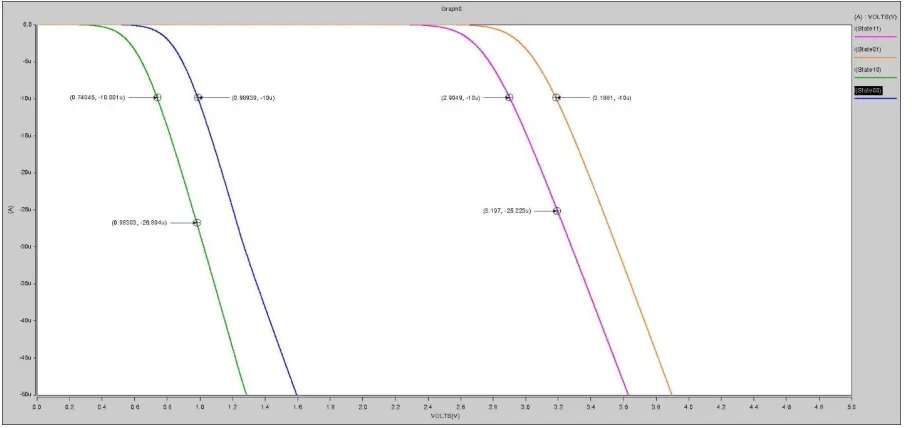
Figure 3.6 Id-Vgs Curve of Four States of double floating gate FET (Vds = 1V)
Table 3-1 Descriptions of Four States of Double Floating Gate
State Description Vth Vth Shift from S00
S00 Uncharged State 0.71V 0.00
S10 Volatile Programmed 0.46V -0.25V
S01 Non-volatile Programmed 2.61V 1.90V
S11 Volatile and non-volatile programmed 2.36V 1.65V
The threshold voltages of all four states are 460mV, 710mV, 2.36V and 2.61V for S10, S00, S11 and S01 respectively. The threshold shift of non-volatile programming to original state is 1.9V. This value is larger than the previous research results and mainly due to the inaccuracy of the Verilog-A model. However, this does not affect the main body of this thesis, in which building the peripheral circuits of the double floating gate FET array to reach certain
CHAPTER 4 PERIPHERAL CIRCUITS DESIGN AND PERFORMANCE OPTIMIZATION
Based on previous work [2] [3], this thesis improved the performances of the peripheral circuits of the double floating gate FET array. The proposed peripheral circuits can access the memory faster. Also a strategy is developed to give accurate control over the threshold voltage of the double floating gate. This not only reduces the errors and in read processes but also increase the efficiency of the system. Macro and micro variations mentioned in [3] can also be relieved by this strategy.
It’s not easy to scale down from 45nm peripheral circuits design into 16nm. The 16nm Predictive Technology Model has a large initial threshold voltage of 0.68V, which is very unsuitable for analog design with power supply of 1V. If current mirror structure is applied using this 16nm Technology, it will be very hard to drive them to work and the slew rate can be very small. However, higher threshold voltage reduces the subthreshold voltage leakage. High threshold 16nm Technology is suitable for digital circuits design due to its faster speed and lower power consumption.
4.1 Systematic Diagrams of Double Floating Gate FET Array
Figure 4.1 Traditional Array-Structured Memory Architecture [4]
The traditional array-structured memory is widely used among SRAM and DRAM arrays. It builds a “standard” template to design peripheral circuits of memories. The row decoder and column decoder jointly select out the desired cell in the memory. The column decoder also connects sense amplifiers for read and drivers for write in this scheme.
back gate of the double floating gate FET, so a new systematic diagram is proposed, shown in Figure 4.2.
Figure 4.2 Systematic Diagram of double floating gate FET Memory
double floating gate FET array. Both the read and write process need the sense amplifier to sense the output. In read cycle, sense amplifier senses the output of the selected cell. In write cycle, sense amplifier is used to carry out “small write” after huge write voltage envelopes. The sense amplifier can distinguish between very small current changes and amplifies it. So it could be exploited to get very accurate threshold voltage control.
4.2 Row and Column Decoder
Figure 4.3 2 Bit NAND Decoder
Table 4-1 MOSFET Sizes and Technologies of Two Input Decoder
Name Size (nm) Technology
M0, M1, M12 16/16 Predictive Technology Model 16nm NMOS
Figure 4.3 shows a typical type of 2 input NAND decoder. Since 16nm Technology is used, NAND type is fast enough to satisfy our needs to access the double floating gate FET array. The double floating gate FET array tested in this thesis exploited a NOR type structure. For 16nm technology, NAND type decoder can be switching within nanoseconds and is fast enough to drive the NOR double floating gate FET array. In Figure 4.3, This 2 bit NAND decoder drives the column when A0 and A1 are asserted. During precharge phase, clock (clk) signal turns on M8, which in turn get the drain of M1 charged to Vdd. During decoding phase, M8 is turned off and the drain of M1 is pulled down close to ground and the inverter has a high output to drive the word line. These two phases are controlled by the controller.
For a very large double floating gate FET array with many devices, it will lead to errors if the number of NMOS in series in a NAND decoder is too large. So many NMOS in series will have a huge equivalent RC network Such as in Figure 4.3, if M1 is followed by many NMOSs to the ground on the left side, the RC time constant will be prominently larger than the frequency of the clock signal and the drain of M1 could not discharge completely. Thus the output of the decoder will not have a proper result.
also apply other strategies like multiple cycles to decode many input bits. However, there is a tradeoff between decoding speed, power consumption and circuitry complexity. The pre-decoding scheme is reconfigurable and easy to implement. It’s fit for usage in verification of large double floating gate FET array. In this thesis, a 4×4 double floating gate FET array is suggested, so 2 bit NAND decoder is enough. The NAND decoder applies for row and column decoder simultaneously.
4.3 Internal Clock Source
An internal clock source is designed to generate pulses of specific width and drive the controller.
Figure 4.4 5 Stage Ring Oscillator
susceptible to negative-bias temperature instability (NBTI), the ring oscillator consumes less power and is easier to apply.
Figure 4.5 Schematic of 5 Stage Ring Oscillator
Table 4-2 MOSFET Sizes and Technologies of VCO
Name Size (nm) Technology
M0 90/50 NMOS_VTL of FreePDK45
M11 250/50 PMOS_VTL of FreePDK45
M2, M4, M5, M18, M21
Table 4-2 continued
M1, M3, M6, M19, M20
110/50 NMOS_VTL of FreePDK45
M13, M15, M16, M23, M24
222.5/50 PMOS_VTL of FreePDK45
M12, M14, M17, M22, M25
250/50 PMOS_VTL of FreePDK45
The 5 stage ring oscillator is built with an enable control. The oscillation frequency of an N stage ring oscillator is
𝑓 = 1/(5 × (𝑡𝑝𝑙ℎ+ 𝑡𝑝ℎ𝑙))
Figure 4.6 Ring Oscillator Simulation Result
It could be seen that when the enable is high, the oscillator starts to work. And it stops working when the enable is pulled down to low. This is more power efficient than a free running clock source.
4.4 Level Shifters
4.4.1 Positive Level Shifter
Figure 4.7 Positive Level Shifter
Table 4-3 MOSFET Sizes and Technologies of Positive Level Shifter
Name Size (nm) Technology
M0, M1 720/50 NMOS_VTL of FreePDK45
M2, M3 1440/50 PMOS_VTL of FreePDK45
M4, M5,
M10, M12
2000/50 NMOS_VTL of FreePDK45
M24, M25 10000/450 Predictive Technology Model 180nm NMOS
Table 4-3 continued
M14 1000/450 Predictive Technology Model 180nm NMOS
M15 5000/450 Predictive Technology Model 180nm PMOS
The positive level shifter uses 45nm and 180nm technology. To increase its driving ability, input buffer M0 to M3 are selected wide enough. No zero threshold voltage transistor is used. When Vin is high, Vinp is high. And the gate of M6 and drain of M8 is pulled down. M6 starts work, which further stops M8 to work by pulling up M8 gate to be high. VO2 is low and the output is high. It’s the same case when Vin is low. The speed of the positive level shifter mainly depends on the driving ability of the input buffer and the driving ability of the cross coupled pair. It’s fast enough to generate a 7V pulse with a delay smaller than 1ns.
4.4.2 Negative Level Shifter
Table 4-4 MOSFET Sizes and Technologies of Negative Level Shifter
Name Size (nm) Technology
M2, M4 720/50 NMOS_VTL of FreePDK45
M3, M5 1440/50 PMOS_VTL of FreePDK45
M6, M1 50000/180 Predictive Technology Model 180nm PMOS
M0, M24 10000/450 Predictive Technology Model 180nm NMOS
M9, M10 10000/450 Predictive Technology Model 180nm NMOS
M7, M8 50000/450 Predictive Technology Model 180nm NMOS
Figure 4.9 Ring Oscillator Driving Positive Level Shifter
Figure 4.9 shows the simulation results of the proposed ring oscillator driving the positive level shifter, which has a high power supply of 6.2V. The 6.2V, 5ns pulse is crucial in building the small write circuit. It shows that the level shifters are very fast.
4.4.3 Multiple Level Shifter Considerations
the inverter changes. Another compensation is to increase the supply voltage, like changing the power supply from 6.5V to 7.5V to drive a 4.2V pull down device of the positive level shifter.
4.5 Sense Amplifier
Figure 4.10 Current Mode Sense Amplifier
Table 4-5 MOSFET Sizes and Technologies of Sense Amplifier
Name Size (nm) Technology
M0, M3, M6 64/16 Predictive Technology Model 16nm NMOS Low Vth
M1, M2 128/16 Predictive Technology Model 16nm PMOS Low Vth
M4, M5 128/16 Predictive Technology Model 16nm NMOS Low Vth
M8 256/16 Predictive Technology Model 16nm NMOS Low Vth
M9, M10 32/16 Predictive Technology Model 16nm NMOS Low Vth
This is a current mode sense amplifier and is very sensitive to the current gap among two inputs. When SE is enabled to drive the equalizer (M6), the source of M0 and M3 will be pulled low enough to inject current. If Icell is larger than Iref, the cross-coupled pair will give more drive on M5 to maintain the current balance among the equalizer, thus the sense amplifier has low output on SAout1 and high output on SAout2.
4.6 Piecewise Linear Write Circuit
Figure 4.11 Precise Write Algorithm [3]
In Figure 4.11, there is an accurate control algorithm of the threshold voltage [3]. It is required to compare the threshold voltage with a standard cell to decide if the threshold voltage difference satisfies our needs, like 250mV to distinguish the volatile state and uncharged state.
4.6.1 Basic Ideas
used to compare and decide the data inside the target cell. In linear region, the current difference between the standard cell and the target cell is proportional to the threshold
voltage difference. In saturation region, the current difference is no longer proportional to the threshold voltage difference. V. Kotipalli’s method [3] assumes accurate control of the work states of devices in linear region and analog to digital converter may be used.
The piecewise linear write method developed in this thesis fully exploits the properties of sense amplifier. Consider the sense amplifier with input current from a target cell with dynamic programmed and the standard cell uncharged. The dynamic programmed the cell will drive more current into the sense amplifier when applied the same gate voltage envelope. If equal currents are wanted to inject into both sides of the sense amplifier, more current needs to be injected together with the standard cell and less current will be injected with the dynamic programmed cell.
Table 4-6 MOSFET Sizes and Technologies of Piecewise Linear Write Circuit
Name Size (nm) Technology
M0, M3, M6 64/16 Predictive Technology Model 16nm NMOS Low Vth
M1, M2 128/16 Predictive Technology Model 16nm PMOS Low Vth
M4, M5 128/16 Predictive Technology Model 16nm NMOS Low Vth
M8 256/16 Predictive Technology Model 16nm NMOS Low Vth
M9, M10 32/16 Predictive Technology Model 16nm NMOS Low Vth
M7, M11 64/16 Predictive Technology Model 16nm PMOS Low Vth
M12, M15,
M16, M19
90/50 NMOS_VTL of FreePDK45
M13, M14,
M17, M17
90/50 NMOS_VTL of FreePDK45
DFG_1, DFG_Ref NA Double Floating Gate FET Model
As in Figure 4.12, if the currents injected into the sense amplifier are pretty close, it can be concluded that the threshold voltage could be defined by the current differences of external current source 1 (CS1) and current source 2 (CS2). The resolution of the bias current decides the accuracy of the piecewise linear write circuit. Thus the threshold voltage shift is
4.6.2 Constant Gm Bias Circuit
Figure 4.13 Constant Gm Bias Network
Table 4-7 MOSFET Sizes and Technologies of Bias Network
Name Size (nm) Technology
M1, M2, M4 90/50 NMOS_VTL of FreePDK45
M0 90/50 NMOS_VTH of FreePDK45
M5 90/50 PMOS_VTL of FreePDK45
M6 90/50 PMOS_VTH of FreePDK45
M7 180/50 PMOS_VTL of FreePDK45
M4 will remain in triode region after start-up. The out2 is defined by the R0 and their relationship could be found in textbooks and journals.
4.6.3 Auxiliary Network in Generating Current
Figure 4.14 Auxiliary Network
Table 4-8 MOSFET Sizes and Technologies of Auxiliary Network
Name Size (nm) Technology
Table 4-8 continued
M42, M44, M45 90/50 PMOS_VTL of FreePDK45
M45, M55,
M56, M57
90/50 NMOS_VTL of FreePDK45
M46 90/50 PMOS_VTL of FreePDK45
M52 180/50 PMOS_VTL of FreePDK45
M53 360/50 PMOS_VTL of FreePDK45
M54 720/50 PMOS_VTL of FreePDK45
The node ConstantGmOut2 is from the Out2 node of Constant Gm Bias. It’s nearly 0.6V. The three triode-connected M45 M44 and M42 are used to define 1uA. Transistors of 45nm and 16nm technologies suffer from the drain induced barriers lowering (DIBL). So the Vds over the transistor has larger impact over the Ids than 180nm and other long channel
technologies. This network defines 1uA, 2uA, 4uA and 8uA. They can be used to generate from 1uA to 15uA with any values among them and a resolution of 1uA. M47, M55, M56 and M57 are specially chosen NMOS. Not only these four transistor can be controlled by the controller to select desired current, they will also protect M46, M52, M54 and M53 from too large Vds variations. Thus making the current definitions as accurate as possible is crucial.
4.6.4 Piecewise-Write Demonstration
Figure 4.15 Simulation of Piecewise Linear Write Circuit
Due to previous error-and-trail results, IBias1 and IBias2 are 1uA and 8uA respectively. Thus the cell will have threshold voltage of -300mV when the flip of the output of sense amplifier happens. To demonstrate the piece-wise linear write strategy, an uncharged double floating gate FET is applied 6.2V 60ns voltage envelope initially. And two 6.2V 5ns envelope is applied between 40ns-60ns and 80ns-100ns respectively. The flip of the sense amplifier is observed. Since the write envelope is so small, the relative error is within controllable range.
4.6.5 Increased Read Noise Margin from Piecewise Linear Write Circuit
It’s easy to distinguish between dynamic programmed device and the not programmed device. However, it’s easy to make errors in deciding when the device is not programmed.
the proper read by applying higher current to reference end. If the current from the bias circuit into the reference end is 1uA higher than the cell end, it’s more likely the sense amplifier have SAout1 high and SAout2 low. This means the “0” is stored inside the cell. The noise must be large enough to overcome the “1uA” barrier. Many more selections like 2uA, 3uA could also be used. The proper operation to building the 1uA barrier is to inject 2uA to the reference end and 1uA to the cell end. This will keep symmetry of the topology and ensure its accuracy.
4.6.6 Reducing the Micro-Level Variation
4.7 Controller Design
As discussed in the thesis before, the running of the whole peripheral circuits are controlled by a controller. A finite state machine (FSM) is assumed. It is able of communicating with other chips like MCUs or some others. First, it should be able to generate pulse with
modulation (PWM) wave. The PWM wave is used to tune the supply voltage of the positive level shifter and negative level shifter, since the output voltage of a Boost Converter is decided by the duty cycle of the PWM wave.
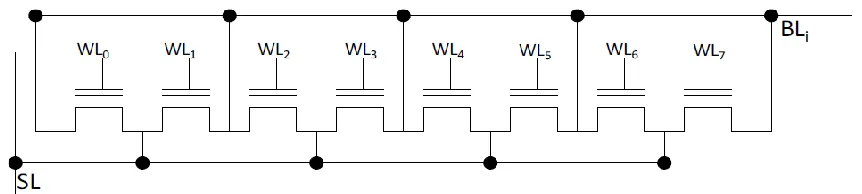
CHAPTER 5 DOUBLE FLOATING GATE FET ARRAY OPERATION
Figure 5.1 Double Floating Gate FET Array
two reference cells are locally selected to get over the macro level process variations. And one of it is not programmed and the other one is non-volatile programmed.
5.1 Operations of Double Floating Gate FET Array
For a read process, at first the non-volatile programmed cell is picked out and applied 1.4V to control gate together with the target cell. If the target cell end has larger current, this means the target cell is not non-volatile programmed. And if the reference cell end has larger current, this means the cell is non-volatile programmed. Here we used the piecewise linear write strategy to overcome the noise. For a non-volatile programmed device, a 3.2V is applied to the control gate to compare with the volatile reference cell. For a device without non-volatile programming, 1V is applied to the control gate. There many reading methods and they depend on different circuits. Like the current multi0-level cell (MLC) used in flash memory, there is a tradeoff between accuracy and storage capability. If a single cycle read is preferred for double floating gate FET, 3.0V to the control gate is desired since the Ids clearly differentiate each other of the four states.
time, when piece-wise linear write strategy is applied, certain settle time should be scheduled by the controller.
5.2 Simulation Process and Results
The Verilog-A model simulation takes up huge amount of disk spaces. For 2 Gigabytes space from NC State University, it’s not possible to wait for 1s with proper time step and no
convergence problems of 18 double floating gate FETs. A possible substitution is to write down the charge on the top and bottom floating gate of four states and simulate the crucial transitions.
The extracted wire resistance and capacitance from Bhattacharyya’s work are included in simulations. After random tests of 16 cells with reads and dynamic writes, it takes 1.03pJ to 1.63pJ to read and 0.7pJ to dynamic write. For the read, 5ns is needed from assert the bit line to the output of the sense amplifier over the SR latch. The refresh time is close to Kotipalli’s work of 180ms. In comparison with Bhattacharyya’s work, higher power consumptions, faster read and smaller refresh rate are reached. It’s not to say this design is superior to his design. Because the change in topologies and design ideas, like this thesis proposed a very sensitive current mode amplifier, which takes higher power consumption and have higher resolution. The double floating gate FET’s source are connected to ground and the current are mirrored through current mirrors into the sense amplifier, which is fundamentally different from Bhattacharyya’s work. Future work needs to apply real library from
CHAPTER 6 CONCLUSIONS AND FUTURE WORK
6.1 Conclusion
A complete, fast and stable peripheral circuits design is finished in this thesis. Macro and micro variations aforementioned [3] are reduced by applying locally generated reference and piece-wise linear write circuits. The core of this thesis is building the piece-wise linear write circuits, which controls the threshold voltage difference between two cells by using
externally defined current source. This method achieves the small write circuit and has an accurate control over the threshold voltage shifts in micro process variation. Also the possibilities of the read error are lowered by setting a hard threshold using this circuit. However, the Verilog-A model used in this thesis is not identical enough to other Verilog-A models, like in Bhattacharyya’s work.
The thesis uses the FreePDK 45nm and Predictive 180nm, 16nm technology to give predictively demonstrative work for the peripheral circuits design. The improvement in technology is avoiding zero threshold voltage transistors by tuning the size of transistors. Faster and accurate read is achieved at the cost of consuming higher power.
6.2 Future work
Future researchers need to keep on finding the best tradeoff between spend and power
REFERENCES
[1] D. Schinke, "Computing with Novel Floating Gates", North Carolina State University, PhD Dissertation, 2011
[2] A. Bhattacharyya, "Design and Optimization of a 16nm Dual Floating Gate FET Memory Array and Peripheral Circuits", North Carolina State University, Master Thesis, 2013 [3] V. Kotipalli, "Impact of Process Variations on 16-nm Dual Floating Gate (DFG) FET
using TCAD Simulations", North Carolina State University, Master Thesis, 2012
[4] W. Rhett Davis, "Array-Structured Memory Architecture", North Carolina University, ECE546 Lecture Notes Ch.13, Fall 2013
[5] N. Di Spigna, Paul D. Franzon, "Emerging Devices", North Carolina State University, ECE733 Lecture Notes, Spring 2014
[6] Predictive Technology Model fromhttp://ptm.asu.edu
[7] Gray, Paul R., Paul Hurst, Robert G. Meyer, and Stephen Lewis. Analysis and design of analog integrated circuits. Wiley, 2001
[8]Rabaey, Jan M., Anantha P. Chandrakasan, and Borivoje Nikolic. Digital integrated circuits. Vol. 2. Englewood Cliffs: Prentice hall, 2002.
[10]Masuoka, Fujio, et al. "New ultra high density EPROM and flash EEPROM with NAND structure cell." Electron Devices Meeting, 1987 International. Vol. 33. IEEE, 1987.
[11]Hutchby, Jim, and Mike Garner. "Assessment of the potential & maturity of selected emerging research memory technologies." Workshop & ERD/ERM Working Group Meeting (April 6-7, 2010).[Online]. Available: http://www. itrs.
Appendix A Verilog-A module
// FUNCTION: Physical Model of Charging/Discharging Nanocrystal Floating Gate // VERSION: $Revision: 2.7 $
// AUTHOR: Cadence Design Systems, Inc. // GENERATED BY: Cadence Modelwriter 2.31 // ON: Tue May 05 13:09:59 EDT 2015
//
`include "discipline.h" `include "constants.h"
module NanocrystalFloatingGate_NCFG_45nm_RefNV (vin, vout); inout vin, vout;
voltage vin, vout;
real psi_week, Qfg_top, Qfg_bottom, n, delta_phi, psi_strong, Vsurface, Vgb_acc, psi_acc, psi_sacc, Vfg_top, Vfg_bottom, VSiO2, ESiO2, phibn, A, B,
J_FN, J_DT, psi_SiO2, Jfg_bottom_to_sub, phibn2, A2, B2, Jsub_to_fg_bottom, VHfO2, EHfO2, phibn3, A3, B3, psi_HfO2, Jcg_to_fg_top, phibn4, A4, B4,
Jfg_top_to_cg, VHfSiO, EHfSiO, phibn5, A5, B5, psi_HfSiO, Jfg_top_to_fg_bottom, phibn6, A6, B6, Jfg_bottom_to_fg_top;
// Physical Constants
parameter real Epi_Si = 11.8*Eo;//Permittivity of silicon [F/m] parameter real Epi_SiO2 = 3.9*Eo; //Permittivity of SiO2 [F/m] parameter real Epi_HfO2 = 17*Eo; //Permittivity of Hfo2 [F/m] parameter real Epi_HfSiO = 25*Eo; //Permittivity of HfSio [F/m] parameter real Mo = 9.10938188e-31; //Free electron mass [kg] parameter real h = 6.62606876e-34; //Planck's constant [m^2*kg/s] parameter real k = 1.38066e-23; //Boltzmann constant [C*V/K] parameter real e = 1.60219e-19; //Electron charge [C]
parameter real pi = 3.141592654; //Mathematical Pi
parameter real kappa = 0.1; //(important for surface potential computation in the accumulation region)
//Device Parameters for calculating direct tunneling and F-N tunneling //For Programming Model
parameter real phi_HfO2_Pt = 2.75; //Maybe I will type in them in the later cases parameter real phi_HfSiO_Mg = 1.25;
parameter real phi_SiO2_Si = 3.15; //For Erasing Model
parameter real Ni = 1.45e16; //Intrinsic carrier concentration of silicon [1/m^-3] parameter real Nbulk = 5e22; //Acceptor concentration in the bulk [1/m^-3] parameter real Nchannel = 4e24; //Acceptor concentration in the channel [1/m^-3] parameter real channel_depth = 0.02e-6; //Channel junction depth [m]
parameter real T = 300; //Temperature
parameter real doxHfO2 = 18n; //Control Gate to Top Floating Gate Oxide Thickness parameter real doxHfSiO = 3.2n; //Top Floating Gate to Bottom Floating Gate Oxide Thickness
parameter real doxSiO2 = 4n; //Bottom Floating Gate to Channel Oxide Thickness parameter real phi_m = 0.1; //Contact potential of control gate to intrinsic silicon parameter real phi_t=k*T/e; //Thermal Voltage [V]
parameter real Qo = 0; //Effective interface charge parameter real gate_length = 45n; //Device gate length parameter real gate_depth = 100n; //Device gate width
parameter real Area = gate_length*gate_depth; //Device gate area //Nanocrystal Parameters (spherical NCs considered)
parameter real nc_diameter = 3.0n;//Diameter of the nanocrystal
parameter real nc_area = pi*(nc_diameter/2)*(nc_diameter/2);//Surface area of the //nanocrystal
parameter real C3 = Epi_HfO2*nc_area/doxHfO2; //Capacitance between the control gate and top floating gate
parameter real C2 = Epi_HfSiO*nc_area/doxHfSiO; //Capacitance between the top floating gate and bottom floating gate
parameter real C1 = Epi_SiO2*nc_area/doxSiO2; //Capactannce between the bottom floating gate and the substrate
//Process Parameters
parameter real const = channel_depth/sqrt(2*(-ln(Nbulk/Nchannel)));//(important for effective channel doping in next line)
parameter real Neff = Nchannel*const*sqrt(2*pi)/(2*channel_depth); //Effective channel doping ( here is from discussing with Dr. Di Spigna)
parameter real gamma = doxSiO2*sqrt(2*Epi_Si*e*(Nbulk+Neff))/Epi_SiO2;//Body effect coefficient I strongly doubt it here
parameter real phi_f = phi_t*ln(Neff/Ni);//Fermi-level
parameter real Vfb = -phi_f-phi_m-Qo*doxSiO2/Epi_SiO2;//Flatband voltage [V]
parameter real GAMMA1 = 1/(1+gamma/sqrt(2*phi_t));//(important for band bending computation in accumulation region
parameter real Eg=1.12; //Silicon bandgap [eV] //Electron Mass in Silicon and SiO2
parameter real moxn = 0.4*Mo; parameter real mHfO2 = 0.17*Mo; parameter real mHfSiO = 0.2*Mo;
parameter real time_step = 1n; analog begin
bound_step(time_step); @(timer(0,0)) begin
Qfg_bottom = 0; //Initial Charge on Bottom Floating Gate Qfg_top = 0; //Initial Charge on Top Floating Gate
//Computation of the initial surface potential and floating gate voltage at time = 0 seconds using equations for the accumulation region from
//Pregaldiny et al, "Accounting for quantum mechanical effects from accumulation to inversion, in a fully analytical surface-potential-based
//MOSFET model," Solid State Electronics, vol 48, pp 781-787, 2004
psi_week= (-gamma/2+sqrt(gamma*gamma/4+V(vin)+Qfg_top/(C3+C2) + Qfg_bottom/(C2+C1)-Vfb))*(-gamma/2+sqrt(gamma*gamma/4+V(vin)+Qfg_top/(C3+C2) + Qfg_bottom/(C2+C1)-Vfb));
n=1+gamma/(2*sqrt(psi_week));
delta_phi = 2*phi_t/n*ln(1+(psi_week-2*phi_f)/(2*phi_t)); psi_strong= 2*phi_f+delta_phi;
if (psi_week <= 2*phi_f) begin //weak inversion region
Vsurface = psi_week-phi_f; end
else begin //strong inversion region
Vsurface = psi_strong-phi_f; end
end
else begin //accumulation region
Vgb_acc =
0.5*(V(vin)+Qfg_top/(C3+C2)+Qfg_bottom/(C2+C1)-
Vfb+sqrt((V(vin)+Qfg_top/(C3+C2)+Qfg_bottom/(C2+C1)-Vfb)*(V(vin)+Qfg_top/(C3+C2)+Qfg_bottom/(C2+C1)-Vfb)+4*kappa*kappa));
psi_acc = GAMMA1*(V(vin)+Qfg_top/(C3+C2)+Qfg_bottom/(C2+C1)-Vfb-
psi_sacc = -phi_t*ln(1-psi_acc/phi_t+(V(vin)+Qfg_top/(C3+C2)+Qfg_bottom/(C2+C1)-
Vfb-Vgb_acc- psi_acc)/(gamma*sqrt(phi_t))*(V(vin)+Qfg_top/(C3+C2)+Qfg_bottom/(C2+C1)-Vfb-Vgb_acc-psi_acc)/(gamma*sqrt(phi_t)));
Vsurface = psi_sacc-phi_f; end
Vfg_top = ((V(vin)+phi_m)*C3+Vfg_bottom*C2)/(C3+C2)+Qfg_top/(C3+C2); Vfg_bottom = (Vfg_top*C2+Vsurface*C1)/(C2+C1)+Qfg_bottom/(C2+C1); end
//Computation of electron tunneling through the tunnel oxide
if (Vfg_bottom >= Vsurface) begin // This is the current from Mg to Si VSiO2 = Vfg_bottom-Vsurface;
ESiO2 = VSiO2/doxSiO2; phibn = 3.15*e;
//Barrier height between SiO2 and the channel surface in the conduction band A = e*e*e*(msin/moxn)/(8*pi*h*phibn);
B = (8*pi*pow(phibn, 1.5)*sqrt(2*moxn))/(3*e*h);
psi_SiO2 = exp(-8*pi*sqrt(2*moxn)*(pow(phibn,1.5)-pow(phibn-e*VSiO2,1.5))/(3*h*e*ESiO2));
J_DT=e*e*e*(msin/moxn)/(8*pi*h*phibn)*ESiO2*ESiO2*psi_SiO2; //Direct tunneling equation
end else begin J_DT=0; end
Jfg_bottom_to_sub=J_FN+J_DT; end
else begin
VSiO2=Vsurface-Vfg_bottom; ESiO2=VSiO2/doxSiO2;
phibn2=2.9*e; //Electron affinity of SiO2 is assumed to be 0.9eV
A2=e*e*e*(msin/moxn)/(8*pi*h*phibn2);
B2=(8*pi*pow(phibn2, 1.5)*sqrt(2*moxn))/(3*e*h); J_FN = A2*ESiO2*ESiO2*exp(-B2/ESiO2);
psi_SiO2 = exp(-8*pi*sqrt(2*moxn)*(pow(phibn2,1.5)-pow(phibn2-e*VSiO2,1.5))/(3*h*e*ESiO2));
J_DT=e*e*e*(msin/moxn)/(8*pi*h*phibn2)*ESiO2*ESiO2*psi_SiO2; end
else begin J_DT=0; end
Jsub_to_fg_bottom=J_FN+J_DT; end
//Computation of electron tunneling through the control gate oxide and floating gate top if (Vfg_top <= V(vin)+phi_m) begin // current from Mo to Pt
VHfO2=V(vin)+phi_m-Vfg_top; EHfO2=VHfO2/doxHfO2; phibn3=2.9*e;
A3=e*e*e*(msin/mHfO2)/(8*pi*h*phibn3);
B3=(8*pi*pow(phibn3, 1.5)*sqrt(2*mHfO2))/(3*e*h); J_FN = A3*EHfO2*EHfO2*exp(-B3/EHfO2);
if (e*VHfO2 < phibn3) begin
psi_HfO2 = exp(-8*pi*sqrt(2*mHfO2)*(pow(phibn3,1.5)-pow(phibn3-e*VHfO2,1.5))/(3*h*e*EHfO2));
end else begin J_DT=0; end
Jcg_to_fg_top=J_FN+J_DT; end
else begin
VHfO2=Vfg_top-(V(vin)+phi_m); // curren from Pt to Mo EHfO2=VHfO2/doxHfO2;
phibn4=1.7*e;
A4=e*e*e*(msin/mHfO2)/(8*pi*h*phibn4);
B4=(8*pi*pow(phibn4, 1.5)*sqrt(2*mHfO2))/(3*e*h); J_FN = A4*EHfO2*EHfO2*exp(-B4/EHfO2);
if (e*VHfO2 < phibn4) begin
psi_HfO2 = exp(-8*pi*sqrt(2*mHfO2)*(pow(phibn4,1.5)-pow(phibn4-e*VHfO2,1.5))/(3*h*e*EHfO2));
J_DT=e*e*e*(msin/mHfO2)/(8*pi*h*phibn4)*EHfO2*EHfO2*psi_HfO2; end
Jfg_top_to_cg=J_FN+J_DT; end
// Computing of electron tunneling through the floating gate top and floating gate bottom if (Vfg_bottom <= Vfg_top) begin // current from Mo to Pt
VHfSiO=Vfg_top - Vfg_bottom; EHfSiO=VHfSiO/doxHfSiO; phibn5=1.25*e;
A5=e*e*e*(msin/mHfSiO)/(8*pi*h*phibn5);
B5=(8*pi*pow(phibn5, 1.5)*sqrt(2*mHfSiO))/(3*e*h); J_FN = A5*EHfSiO*EHfSiO*exp(-B3/EHfSiO); if (e*VHfSiO < phibn5) begin
psi_HfSiO = exp(-8*pi*sqrt(2*mHfSiO)*(pow(phibn5,1.5)-pow(phibn5-e*VHfSiO,1.5))/(3*h*e*EHfSiO));
J_DT=e*e*e*(msin/mHfSiO)/(8*pi*h*phibn5)*EHfSiO*EHfSiO*psi_HfSiO; end
else begin J_DT=0; end
else begin
VHfSiO=Vfg_bottom - Vfg_top; EHfSiO=VHfSiO/doxHfSiO; phibn6=3.10*e;
A6=e*e*e*(msin/mHfSiO)/(8*pi*h*phibn6);
B6=(8*pi*pow(phibn6, 1.5)*sqrt(2*mHfSiO))/(3*e*h); J_FN = A6*EHfSiO*EHfSiO*exp(-B3/EHfSiO); if (e*VHfSiO < phibn6) begin
psi_HfSiO = exp(-8*pi*sqrt(2*mHfSiO)*(pow(phibn6,1.5)-pow(phibn6-e*VHfSiO,1.5))/(3*h*e*EHfSiO));
J_DT=e*e*e*(msin/mHfSiO)/(8*pi*h*phibn6)*EHfSiO*EHfSiO*psi_HfSiO; end
else begin J_DT=0; end
Jfg_bottom_to_fg_top = J_FN + J_DT; end
psi_week= (-gamma/2+sqrt(gamma*gamma/4+Vfg_bottom+phi_f))*(-gamma/2+sqrt(gamma*gamma/4+Vfg_bottom+phi_f));
n=1+gamma/(2*sqrt(psi_week));
delta_phi = 2*phi_t/n*ln(1+(psi_week-2*phi_f)/(2*phi_t)); psi_strong= 2*phi_f+delta_phi;
if (psi_week <= 2*phi_f) begin Vsurface = psi_week-phi_f; end
else begin
Vsurface = psi_strong-phi_f; end
end else begin
Vgb_acc =
0.5*(Vfg_bottom+phi_f+sqrt((Vfg_bottom+phi_f)*(Vfg_bottom+phi_f)+4*kappa*kappa));
psi_acc =
GAMMA1*(Vfg_bottom+phi_f-
Vgb_acc)/(sqrt(1+GAMMA1*(Vfg_bottom+phi_f-Vgb_acc)/(4*phi_t)*GAMMA1*(Vfg_bottom+phi_f-Vgb_acc)/(4*phi_t)));
end
//Computing of the new floating gate charge and voltage after each iteration
// Qfg=Qfg-(Jin_sub+Jin_cgate-Jout_sub - Jout_cgate)*nc_area*Rnc*time_step; // Vfg=((V(vin)+phi_m)*Ccgox+Vsurface*Ctox)/(Ctox+Ccgox)+Qfg/(Ctox+Ccgox);
Qfg_bottom =
Qfg_bottom-(Jfg_bottom_to_sub-Jsub_to_fg_bottom+Jfg_bottom_to_fg_top-Jfg_top_to_fg_bottom)*3*Area*time_step; Qfg_top = Qfg_top-(Jfg_top_to_fg_bottom-Jfg_bottom_to_fg_top+Jfg_top_to_cg-Jcg_to_fg_top)*3*Area*time_step;
Vfg_top = ((V(vin)+phi_m)*C3+Vfg_bottom*C2)/(C3+C2)+Qfg_top/(C2+C3); Vfg_bottom = (Vfg_top*C2+Vsurface*C1)/(C1+C2)+Qfg_bottom/(C1+C2);
V(vout) <+ Vfg_bottom; //The output of this Verilog-A model is the floating gate voltage, which is then connected to the gate terminal of a MOSFET to complete the physical model
begin
$strobe("Number Ref NV Charge per Nanocrystal Bottom Floating Gate = %e, time is %e", Qfg_bottom, $realtime);
$strobe("Number Ref NV Charge per Nanocrystal Top Floating Gate= %e", Qfg_top); end
end
Appendix B VCO
// this is the voltage controlled oscillator ** Generated for: hspiceD
** Generated on: May 5 22:18:40 2015 ** Design library name: Tutorial
** Design cell name: VCO ** Design view name: schematic
/////v3 net05 0 PULSE 0 1.0 20e-9 10e-12 10e-12 5e-9 10e-9 .GLOBAL vdd!
.tran 1p 1000n
.include '$PDK_DIR/ncsu_basekit/models/hspice/hspice_nom.include'
.TEMP 25.0 .OPTION + ARTIST=2 + INGOLD=2
+ PARHIER=LOCAL + PSF=2
** Library name: Tutorial ** Cell name: VCO ** View name: schematic
** Library name: Tutorial ** Cell name: VCO ** View name: schematic
m23 net023 net019 net036 vdd! PMOS_VTL L=50e-9 W=222.5e-9 AD=23.3625e-15 AS=23.3625e-15 PD=432.5e-9 PS=432.5e-9 M=1
m22 net036 net6 vdd! vdd! PMOS_VTL L=50e-9 W=250e-9 AD=26.25e-15 AS=26.25e-15 PD=460e-9 PS=460e-9 M=1
m15 net14 net8 net42 vdd! PMOS_VTL L=50e-9 W=222.5e-9 AD=23.3625e-15 AS=23.3625e-15 PD=432.5e-9 PS=432.5e-9 M=1
m25 net035 net6 vdd! vdd! PMOS_VTL L=50e-9 W=250e-9 AD=26.25e-15 AS=26.25e-15 PD=460e-9 PS=460e-9 M=1
m11 net6 net6 vdd! vdd! PMOS_VTL L=50e-9 W=250e-9 AD=26.25e-15 AS=26.25e-15 PD=460e-9 PS=460e-9 M=1
m13 net8 vout net43 vdd! PMOS_VTL L=50e-9 W=222.5e-9 AD=23.3625e-15 AS=23.3625e-15 PD=432.5e-9 PS=432.5e-9 M=1
m14 net42 net6 vdd! vdd! PMOS_VTL L=50e-9 W=250e-9 AD=26.25e-15 AS=26.25e-15 PD=460e-9 PS=460e-9 M=1
m12 net43 net6 vdd! vdd! PMOS_VTL L=50e-9 W=250e-9 AD=26.25e-15 AS=26.25e-15 PD=460e-9 PS=460e-9 M=1
m16 net019 net14 net41 vdd! PMOS_VTL L=50e-9 W=222.5e-9 AD=23.3625e-15 AS=23.3625e-15 PD=432.5e-9 PS=432.5e-9 M=1
m17 net41 net6 vdd! vdd! PMOS_VTL L=50e-9 W=250e-9 AD=26.25e-15 AS=26.25e-15 PD=460e-9 PS=460e-9 M=1
m19 net023 net019 net037 0 NMOS_VTL L=50e-9 W=110e-9 AD=11.55e-15 AS=11.55e-15 PD=320e-9 PS=320e-9 M=1
m18 net037 net05 0 0 NMOS_VTL L=50e-9 W=90e-9 AD=9.45e-15 AS=9.45e-15 PD=300e-9 PS=300e-9 M=1
m2 net38 net05 0 0 NMOS_VTL L=50e-9 W=90e-9 AD=9.45e-15 AS=9.45e-15 PD=300e-9 PS=300e-9 M=1
m21 net034 net05 0 0 NMOS_VTL L=50e-9 W=90e-9 AD=9.45e-15 AS=9.45e-15 PD=300e-9 PS=300e-9 M=1
m1 net8 vout net38 0 NMOS_VTL L=50e-9 W=110e-9 AD=11.55e-15 AS=11.55e-15 PD=320e-9 PS=320e-9 M=1
m6 net019 net14 net36 0 NMOS_VTL L=50e-9 W=110e-9 AD=11.55e-15 AS=11.55e-15 PD=320e-9 PS=320e-9 M=1
m4 net37 net05 0 0 NMOS_VTL L=50e-9 W=90e-9 AD=9.45e-15 AS=9.45e-15 PD=300e-9 PS=300e-9 M=1
m0 net6 net05 0 0 NMOS_VTL L=50e-9 W=90e-9 AD=9.45e-15 AS=9.45e-15 PD=300e-9 PS=300e-9 M=1
m20 vout net023 net034 0 NMOS_VTL L=50e-9 W=110e-9 AD=11.55e-15 AS=11.55e-15 PD=320e-9 PS=320e-9 M=1
m3 net14 net8 net37 0 NMOS_VTL L=50e-9 W=110e-9 AD=11.55e-15 AS=11.55e-15 PD=320e-9 PS=320e-9 M=1
v3 net05 0 PULSE 0 1.0 20e-9 10e-12 10e-12 100e-9 200e-9 v0 vdd! 0 DC=1
Appendix C Positive Level Shifter ** Generated for: hspiceD
** Generated on: Mar 18 17:29:26 2015
** Design library name: Tutorial
** Design cell name: levelshiftpos
** Design view name: schematic
.GLOBAL vdd!
.include '$PDK_DIR/ncsu_basekit/models/hspice/hspice_nom.include'
.include "/afs/unity.ncsu.edu/users/j/jjiang11/thesis/Predictive180NMOS.scs"
.include "/afs/unity.ncsu.edu/users/j/jjiang11/thesis/Predictive180PMOS.scs"
.include "/afs/unity.ncsu.edu/users/j/jjiang11/thesis/Predictive180NMOSZeroVt.scs"
.include "/afs/unity.ncsu.edu/users/j/jjiang11/thesis/Predictive180PMOSZeroVt.scs"
.TEMP 25.0
.OPTION
+ INGOLD=2
+ PARHIER=LOCAL
+ PSF=2
+ POST
.tran 1p 200n
** Library name: Tutorial
** Cell name: levelshiftpos
** View name: schematic
m25 o2 inp net027 vddq Predictive180NMOS L=450e-9 W=10e-6
m24 o1 inn net028 vddq Predictive180NMOS L=450e-9 W=10e-6
m14 vout o2 0 0 Predictive180NMOS L=180e-9 W=1e-6
m15 vout o2 vddq vddq Predictive180PMOS L=180e-9 W=5e-6
m8 o2 o1 vddq vddq Predictive180PMOS L=450e-9 W=2e-6
m6 o1 o2 vddq vddq Predictive180PMOS L=450e-9 W=2e-6
v0 vdd! 0 DC=1
m3 inp inn vdd! vdd! PMOS_VTL L=50e-9 W=1.44e-6 AD=151.2e-15 AS=151.2e-15 PD=1.65e-6 PS=1.65e-6 M=1
m2 inn vin vdd! vdd! PMOS_VTL L=50e-9 W=1.44e-6 AD=151.2e-15 AS=151.2e-15 PD=1.65e-6 PS=1.65e-6 M=1
m12 net029 inp 0 0 NMOS_VTL L=50e-9 W=2e-6 AD=210e-15 AS=210e-15 PD=2.21e-6 PS=2.21e-6 M=1
m10 net027 vdd! net029 0 NMOS_VTL L=50e-9 W=2e-6 AD=210e-15 AS=210e-15 PD=2.21e-6 PS=2.21e-6 M=1
m5 net030 inn 0 0 NMOS_VTL L=50e-9 W=2e-6 AD=210e-15 AS=210e-15 PD=2.21e-6 PS=2.21e-6 M=1
m4 net028 vdd! net030 0 NMOS_VTL L=50e-9 W=2e-6 AD=210e-15 AS=210e-15 PD=2.21e-6 PS=2.21e-6 M=1
m1 inp inn 0 0 NMOS_VTL L=50e-9 W=720e-9 AD=75.6e-15 AS=75.6e-15 PD=930e-9 PS=930e-9 M=1
m0 inn vin 0 0 NMOS_VTL L=50e-9 W=720e-9 AD=75.6e-15 AS=75.6e-15 PD=930e-9 PS=930e-9 M=1
v2 vin 0 PULSE 0 1.0 3e-9 10e-11 10e-11 65e-9 100e-9
Appendix D Negative Level Shifter ** Generated for: hspiceD
** Generated on: Mar 19 16:42:48 2015
** Design library name: Tutorial
** Design cell name: levelshiftneg
** Design view name: schematic
.GLOBAL vdd!
.include '$PDK_DIR/ncsu_basekit/models/hspice/hspice_nom.include'
.include "/afs/unity.ncsu.edu/users/j/jjiang11/thesis/Predictive180NMOS.scs"
.include "/afs/unity.ncsu.edu/users/j/jjiang11/thesis/Predictive180PMOS.scs"
.include "/afs/unity.ncsu.edu/users/j/jjiang11/thesis/Predictive180NMOSZeroVt.scs"
.include "/afs/unity.ncsu.edu/users/j/jjiang11/thesis/Predictive180PMOSZeroVt.scs"
.TEMP 25.0
![Figure 2-1 Traditional 1T DRAM from [4]](https://thumb-us.123doks.com/thumbv2/123dok_us/1636171.1204209/17.612.228.404.336.542/figure-traditional-t-dram-from.webp)
![Figure 2-2 6T SRAM [4]](https://thumb-us.123doks.com/thumbv2/123dok_us/1636171.1204209/19.612.114.491.289.576/figure-t-sram.webp)
![Table 2-1 Comparison between the Flash memory and Emerging Nonvolatile Memory Alternatives [1]](https://thumb-us.123doks.com/thumbv2/123dok_us/1636171.1204209/22.612.87.536.176.540/table-comparison-flash-memory-emerging-nonvolatile-memory-alternatives.webp)
![Figure 2-3 Schematic Cross-Section of a Continuous Floating Gate Device [1]](https://thumb-us.123doks.com/thumbv2/123dok_us/1636171.1204209/23.612.190.438.130.318/figure-schematic-cross-section-continuous-floating-gate-device.webp)
![Figure 2-6 Cross-Selection of 16nm Double Floating Gate [1]](https://thumb-us.123doks.com/thumbv2/123dok_us/1636171.1204209/27.612.91.538.289.659/figure-cross-selection-nm-double-floating-gate.webp)
![Figure 3.2 Capacitor Model of Double Floating Gate FET [1]](https://thumb-us.123doks.com/thumbv2/123dok_us/1636171.1204209/33.612.168.470.354.585/figure-capacitor-model-of-double-floating-gate-fet.webp)
![Figure 3.4 Flowchart for Physical Model Computation [1]](https://thumb-us.123doks.com/thumbv2/123dok_us/1636171.1204209/35.612.199.452.249.634/figure-flowchart-physical-model-computation.webp)
![Figure 3.5 Band diagram of universal memory device in (a) program mode, (b) erase mode [1]](https://thumb-us.123doks.com/thumbv2/123dok_us/1636171.1204209/36.612.100.519.329.555/figure-band-diagram-universal-memory-device-program-erase.webp)