On-Chip Generation of Functional Tests
with Reduced Delay and Power
Hemanth Kumar Motamarri 1, Dr.B. Leela Kumari 2
P.G. Student, Department of Electronics and Communication Engineering, JNTU Kakinada University, Kakinada, Andhra Pradesh, India1
Assistant Professor, Department of Electronics and Communication Engineering, JNTU Kakinada University, Kakinada, Andhra Pradesh, India 2
ABSTRACT: This paper describes different methods on-chip test generation method for functional tests. The hardware was based on application of primary input sequences in order to allow the circuit to produce reachable states. Random primary input sequences were modeled to avoid repeated synchronization and thus yields varied sets of reachable states by implementing a decoder in between circuit and LFSR. The on-chip generation of functional tests require simple hardware and achieved high transition fault coverage for testable circuits. Further, power and delay can be reduced by using Bit Swapping LFSR(BS-LFSR).This technique yields less number of transitions for all pattern generation. Bit-swapping(BS) technique is less complex and more reliable to hardware miscommunications.
KEYWORDS: Built-in test generation, functional tests, reachable states, Bit Swapping LFSR(BS-LFSR).
I. INTRODUCTION
Testing of a circuit becomes complex when it is tested in non functional mode. Detection of faults during non functional mode can be termed as over testing which is not desirable. This process consumes a lot of power than the power consumed while testing the design during functional operation. If an arbitrary state is used as scan-in state, a pattern test can bring the circuit under test through state transitions which can’t occur during functional operations. In non functional mode as current requirement is higher than the current required in functional operation may cause voltage drops which may slow down the speed of the circuit and also may fail. In order to avoid such type of cases functional mode is very useful for testing the circuit.
Functional tests are the tests that are applied to the design during its functionality and produce a reachable state to detect the faults present. As functional tests, they operate the circuit in functional mode after an initial state is scanned in. This results in the application of a pattern test. Since the scan-in state is a reachable state, the pattern test takes the circuit through state-transitions that are guaranteed to be possible during functional operation. Delay faults that are detected by the test can also affect functional operation, and the current demands do not exceed those possible during functional operation. This alleviates the type of over testing. In addition, the power dissipation during fast functional clock cycles of functional tests does not exceed that possible during functional operation.
But it i s v e r y c l e a r that the delay fault coverage achieved using functional tests is normally, lower than the coverage achieved using arbitrary tests and pseudo-functional tests described in[3]. The main reason is that the functional tests avoid the unreachable tests,where as the other methods cannot avoid the unreachable states. However, the tests that are needed for achieving this higher fault coverage areal so ones that can cause over testing. They can also dissipate more power than possible during functional operation. Only functional tests are considered in this work.
Under the proposed on-chip test generation method, the circuit is used for generating reachable states during test application. This alleviates the need to compute reachable states or functional constraints by an offline process. The underlying observation is related to one of the methods used for offline test generation, and is the following. Initially if a primary input sequence say H which is applied in functional mode starts from a reachable state, then all the states that can be produced using H will also become reachable states. Now the on-chip test generation using this sequence H achieves high fault coverage. But the number of faults E will be generally high. Let it be represented in |E| as magnitude form. So the reachable states produced using H may not achieve the complete fault coverage, but may be closer to |E|.
The hardware used in this paper for generating the primary input sequence H consists of a linear-feedback shift-register (LFSR)as a random source[4],and some gates of some required number in order to make the sequence compatible with the design. The usage and application of this
gates should be such that the further produced sequences should be synchronization free. This is termed as avoiding repeated synchronization. The advantage of this is to produce different types and patterns of reachable states. The required parameters are the following
1) The number of LFSR bits. 2) Primary input sequence length H.
3) The specified gates used to modify the LFSR sequence in to sequence H.
4) Seeds for the LFSR in order to generate several primary input sequences and several subsets of tests.
The on-chip test generation hardware is based on the one described in[4].It differs from it in the following ways. 1)The logic that is used to produce the primary input sequence H designed such that the LFSR should have the length of atleast n + mod bits,where n is nothing but the length of the primary input sequence of the design and mod is the mod value of the input sequence H.For example if input bit sequence H is 4 bit length then n value is 4 and mod value is 2.
And now the total LFSR length required is 6.Here the MSB n value is used to apply the input to the design and the LSB mod value is used to modify the sequence H.Due to this some sequences are just the shifted values of the previous ones which introduces some dependencies.
In order to reduce the above dependencies disadvantages the minimum length of the LFSR should be (d.n) bit where d > mod.So on considering the above example the minimum length of the LFSR here should be (3.4) =12, where 3 >mod(2) and length of primary input sequence is 4.This is the minimum length required for an LFSR to produce the tests in order to avoid synchronization problems as dependencies of the patterns on the shifted values of the preceding ones. The unused values in (d.n) length of the LFSR are used to avoid the synchronization problems. Due to this it is possible to produce many reachable states using the primary input sequence H. In addition to this other parts of hardware used for test generation can be simplified with the design, as discussed below.
2) The test patterns generated are of different length to control the number of tests applied to the circuit. But in this paper the tests are of uniform length so that the entire process is uniform. The hardware used for the test generation is simple and fixed here and generates the sequences which can be stored on-chip.
When the circuit under test which is to be tested is embedded in a large design then there may be a chance that its primary inputs may be driven by some other logic blocks and also the primary outputs of this circuit under test may drive another logic block. Functional constraints on primary input sequences can be accommodated in one of the following ways.
2) A separate logic block can be used to modify H in order to satisfy the functional constraints. This paper is organized as follows. Section II gives an overview of the on-chip generation and application of functional tests. Section III describes the details.
II.OVERVIEW
This section gives an over view regarding the one chip generation of functional tests. The below is the design which we are testing in this paper.I0,I1,I2,I3 are the inputs i.e of 4 bit length. Three flipflops shown in the design represent the state of the design. The initial state of this design will be 000 which is achieved by asserting a reset input. The initial state can be represented
Fig.1.Circuit under test by sr. The functional operation starts by assuming the from the state sr.
The state changes from sr to si on application of primary input sequence to the input pins mentioned above,H=a(0)a(1) ….a(L-1)
of length L in functional mode. The design reaches from state sr to su at time unit u, where 0 ≤ u ≤ L. So s(0)=sr.
Therefore every state s(u) can be used as intial state for a test t(u) = (s(u),a(u),a(u+1)).By using a(u) and a(u+1) for a single it is possible to detect the synchronization problems while testing.
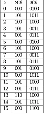
For illustration consider the below table.Table1 yields the functional tests as t(0) = (000,0100,1011),t(1) = (101,1011,1000) …..,t(14) = (101,1011,1100).So it can be formulated as t(u) = (s(u),a(u),a(u+1)).At time unit u the circuit is in state s(u).A fault can be detected in one of the following two ways.
TABLE I FUNCTIONAL TESTS u s(u) a(u)
0 000 0100 1 101 1011 2 100 1000
1) Based on the primary output vectorz(u+1) obtained in response to a(u+1),if this vector is different from the expected fault free primary output vector.
2) Based on the final state s(u+2) of the state,if this state is different from the expected fault free state.
It should be noted that the tests starting in two consecutive time units, u and u+1,are overlapping in the following sense. Application of t(u) takes the circuit through states s(u),s(u+1),s(u+2).Application of t(u+1) takes the circuit through states s(u+1),s(u+2),s(u+3).Application of both t(u) andt(u+1) require special hardware to bring back the circuit to state s(u+1) after t(u) is applied. To avoid the need of this hardware, the proposed test generation hardware applies subsets of non-overlapping tests of the form {t(u0),t(u1),…,t(uk-1)},where ui+1 < ui+1 for 0 ≤ i<k – 1.
Parameter Description
L The length of the Primary input sequence. D Number of LFSR bits for 1 Primary input. Mod Number of LFSR bits required to modify
the value of input sequence. sel Describes the start of test sequences at
Time units based on it. TABLE II Parameters
III. ON-CHIP GENERATION OF FUNCTIONAL TESTS
This section describes the on-chip generation method of functional tests based on the concepts discussed in Section II.
A. PRIMARY INPUT SEQUENCE H
The easiest way to generate the input sequences is to use a LFSR.The input sequence brings the circuit from a known state sr to the set of reachable states.Let a primary input cube c synchronizes a subset of state variables S(c) if the following conditions are satisfied.Let c be applied to the circuit whose intial states are unknown.Then this cube brings the circuit to a next state termed as s,and the values specified in s can be included in S(c).
Let us consider the example that is present in this paper i.eS27 circuit.Let the primary input cube applied to it be I0I1I2I3= 0xxx and the initial state be y0y1y2= xxx,results in the next state Y0Y1Y2= 0xx i.e synchronizing the state variable y0.Similarly,if an input cube I0I1I2I3= xx1x is applied in present state y0y1y2= xxx results in the next state Y0Y1Y2= xx0,synchronizing the state variable y2.
A primary input cube c having less number of specified values is likely to appear repeatedly in a random primary input sequence H.If this happens the state variable in S(c) assume that the same values are repeated in H.This prevents the circuit from entering in to some reachable states and then reduces the ability to detect faults resulting in less fault coverage.
The on-chip test generation hardware uses c for the generation of H = a(0)a(1)a(2) …..a(L-1) as follows.For a circuit with n primary inputs and for parameters d and mod such that d > mod, the hardware includes a (d.n) – bit LFSR.
Here the LFSR is clocked for every L cycles to produce a sequence of length L.
1) The first bit produced is mostly seen to be 1 by using an “OR” gate.This gate increases the chance to produce the bit “1”.
2) The second and fourth bit could be any either 0 or 1.For this the values are just used by a wire without using any modifying logic as seen above.
3) The third bit is seen to be “0”.For this we are using an AND gate which increases the probability to get the value as “1”.
So from above we can observe that the values adjacent to each other being equal have the probabilities less than or equal to 50% only.With this above implementation we can reduce the dependencies between the values of different primary inputs further.
Fig.2. On-chipgenerationof Input sequence H.
Let us see the illustration from Fig 2. The hardware used for s27 with parameters d = 3 and mod = 2,n = 4and c = 1x0x.Here c(0) = 1,c(1) = x,c(2) = 0,c(3) = x.Since c(0) = 1,an OR gate is used to produce 1 which increases the probability of getting 1 for I0.So bits 0,1,2 of LFSR are used to produce I0.Bit 2 of LFSR reduces the dependencies between the I0and I1 values.
Bits 3,4,5 of LFSR are used to produce the value of I1. As the value of c(1) is x so just the bit 3 is driven directly to deduce the value of I1.Bits 4,5 reduce the dependencies between the values of I1and I2.
Bits 6,7,8 are used to produce the value of I2.The value of c(2) mentioned is 0.So AND gate is used to increase the probability of producing the value as 0.Bit 8 is used to reduce the dependencies between the values of I2 and I3.
Bits 9,10,11 of LFSR are used to produce the value of I3.For I3,c(3) = x.So the bit 9 of LFSR is driven directly to produce the value for I3.In general,if there are N primary inputs Ij with c(j) ≠ x,the implementation illustrated by Fig.2 requires a(d.n)- bit LFSR,and N AND or OR gates with mod inputs. Here in this paper the seed used in this pattern for 12 bit LFSR is x12+ x9+ x7 + x5 + x2+ 1i.ethe seed used is 010 011 101 111.
Pattern Generation Techniques
1.Exhaustive method. 2.Pseudo Exhaustive method. 3.Segmentation method. 4.Using BS-LFSR.
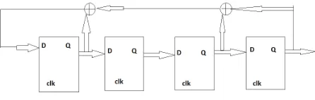
Fig – 3: LFSR
This is one of the exhaustive methods used to generate the test patterns using LFSR. The figure shown represents the polynomial stated above. The selected values from particular FF’s are exored and fed as feed back at the final D-FF.In some industries it is referred as a simple shift register generator (SSRG). This can also be termed as external feedback register due to the presence of EXOR gates outside the LFSR design.
Fig – 4:EXTERNAL FEED BACK LFSR
The above figure shows an illustration of external feed back shift register as exor gates are present outside. 1.b)Binary counter
Fig – 5: COUNTER
Counter can also be used as a technique in generating the test patterns for the design mentioned s-27.Initially to generate the 12-bit patterns we need 12 FF’s. It is very exhaustive method as it consumes a lot of power.The disadvantages in producing the test patterns using this method are as below.
1) The values can be of same throughout the pattern as 12 zeros or 12 ones.
2) The power consumption will be high for more number ofones in the pattern produced.
4) It cannot determine multiple errors present in the design due to synchronization problem.To avoid this problem 4 bit counter can be used whose outputs are directly fed as inputs to the design without using a decoder.But synchronization problem can’t be avoided completely.
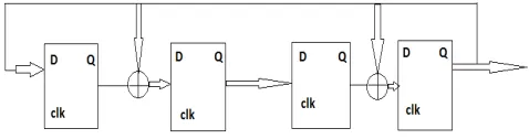
5) It cannot determine the state of the design too. 2.Modulo LFSR
This is an improvement when compared with the standard LFSR.This is more favored form than that of standard LFSR due to absence of gates in the feedback path.This ultimately increases the speed.The patterns generated using both standard LFSR and Modulo LFSR will be generally equal if the initial seed given is same.It is also called as internal feedback shift register due to the presence of exor gates just beside the FF’s which can be shown as below.
Fig – 6:INTERNAL FEED BACK LFSR 3.Segmantation
3.a)Segmentation of design
The design under test is s27 circuit.This is of 4 bit input.
Here the patterns are applied in parts i.ethe design is divided in to two equal halves.One half consists of two inputs and the other half consists of other two inputs.
In order to use decoder,six counters will be used to produce the first two inputs of the design and six more counters
will be used to produce two remaining inouts of the design.
The disadvantages in producing the test patterns using this method are as below. 1) The values can be of same throughout the pattern as 6 zeros or 6 ones.
2) The power consumption will be high for more number ofones in the pattern produced.
3) The number of transitions can also be very high in the patterns produced using a counter rather than LFSR. 4) It cannot determine multiple errors present in the design due to synchronization problem.This problem can be
avoided by using two 2 bit counters and no decoder,but the problem that arises is it can’t determine many faults due to same type of outputs from the counters.
5) It cannot determine the state of the design too. 3.b)Segmentation of polynomial
Fig – 7:SEGMENTED POLYNOMIAL
This method also has some disadvantages i.e it cannot determine multiple faults in the design.It cannot determine the state of the design due to synchronization problem.
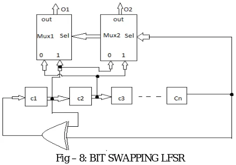
4.Bit Swapping – LFSR
For every primary input sequence this paper needs its corresponding LFSR sequence. The main advantage of this bit swapping LFSR is generation of additional 12 bit sequence with the existing LFSR sequence. This additional sequence is produced by using the bit swapping logic which is explained below. These are combinational outputs i.e fast outputs which reduce the required time and power consumption.
Structure and Working: The bit – swapping LFSR(BS-LFSR) is composed of an LFSR and a 2 x 1 multiplexer. It is used to generate test patterns for scan-based built-in self-tests, which reduces the number of transitions. If the most LSB bit of the
LFSR 12 bit pattern is zero then bit swapping logic is activated, i.e the most MSB bit 11 is swapped with bit 10,bit 9 is swapped with bit 8,bit 7 with bit 6,bit 5 with bit 4,bit 3 with bit 2 and the bits at position 1 and 0 remain same. Thus an additional sequence is produced. The proposed BS-LFSR generates the same number of 1’s and 0’s at the output of multiplexers after swapping of two adjacent cells, hence the probabilities of having a 0 or 1 at a certain cell of the scan chain before applying the test vectors are equal. Hence the proposed design retains an important feature of random TPG.
Fig – 8: BIT SWAPPING LFSR
8.Both the results, one with 12 bit BS LFSR and with 8 bit BS LFSR are produced and compared which can be seen in the results table below.
Advantages of BS-LFSR.
1)Time consumption can be reduced as this paper makes use of combinational outputs.
2)More errors can be determined as many test patterns can be generated than normal LFSR in a fixed amount of time. This reduces the power consumption also.
B. TEST SELECTION
This subsection describes the selection of the functional tests that will be applied based on a primary input sequence H.In order to detect the set of target faults F the tests should be applied at time units U = {u0,u1,u2,…,uk-1} and apply a test set T(U) = {t(ui) : uiϵ
U},where t(ui) = (s(ui),a(ui),a(ui+ 1)) where the tests should be non overlappingi.eui +1 < ui+1 for 0 ≤ I < k-1.
Here in this paper all the tests produced T(U) are applied consecutively i.e tests applied are multiples of 1 as we considered sel
line value as 0i.e tests are applied according to the 2sel.Here it is 20 = 1.If sel line value = 2 then tests are applied at time units which are multiples of 4 as 22 = 4.
C. SELECTING SEEDS
Different seeds yield different primary sequences and different tests.So different seeds are needed to increase the fault coverage.The process in this for selecting seeds is as follows.
1) Let F = set of target faults.For i = 0,1,2,… Let a seedi is a random seed computes the primary input sequence H iand finds the subset of tests Ti(U).If any faults are detected ,it stores the seedi in a set denoted “SEED”.It then continues to consider additional seeds until the last Q seeds do not improve the fault coverage,for a constant Q.
2) Set of SEED = {seed0,seed1,…,seedk-1} with corresponding sequences H0,H1,…,Hk-1. And subsets of applied tests
T0(U),T1(U),…,Tk-1(U).If a fault is detected by Ti(0) then generally seedi is stored.But the same fault is detected by seedi+1 then the
seedi is not considered.
3) If a fault F is detected by seedifrom test Ti(U) then det(f)= Ii.evalidi= 1for 0 ≤ i< k for i = 0,1,…k-1.Now another seedj is considered for j ≠ i,it is tested by subsets Tj(U) and validj = 1.This process continues until the fault is 0,i.e validi = 0.Here the seed used in this pattern for 12 bit LFSR is x12+ x9+ x7 + x5 + x2+ 1i.e the seed used is 101 011 100 100.
The patterns generated can be shown from the TABLE III below. u lfsr(u) 0 010 011 101 111 1 101 001 110 111 2 110 100 111 011 3 111 010 011 101 4 111 101 001 110 5 011 110 100 111 6 001 111 010 011 7 000 111 101 001 8 000 011 110 100 9 100 001 111 010 10 110 000 111 101 11 011 000 011 110 12 001 100 001 111 13 000 110 000 111 14 000 011 000 011 15 100 001 100 001
D. SELECTING PARAMETERS
The parameters are L,d,mod,sel.
1) Mod: It is generally used to modify the input vector.It is normally 3 or 4.The values other than 3 or 4 reduces the fault coverage.Mod value used in this paper is 2.
2) L: This value is normally high as it depends on length of primary input sequence H and mod value.The higher the value of L then the fault coverage will also be high.
3) d:This value is higher than that of mod value.As this value increases the fault coverage also increases.d value used in this paper is 3 which is greater than mod value=2.
4) sel:The value of sel used here is 0.As its value increases the fault coverage will be decreased as the number of tests applied to test the circuit will be reduced.
IV. EXPERIMENTAL RESULTS
Operating Conditions
Global Operating Voltage = 0.7 V Power-specific unit information :Voltage Units = 1V Capacitance Units = 1.000000ff
Time Units = 1ns Dynamic Power Units = 1uW (derived from V,C,T units) Leakage Power Units = 1pW Total Power Units = 1uW.Maximum operating conditions are used in this paper.The technology files used in this paper is 90nm.Clock period used is 37 ns.The time column indicates the data arrival time.Higher the value faster is the implementation of design.Input delay is 15.0 Output delay is 15.0
The results are noted using synopsys DC compiler.
TABLEIV – RESULTS ANALYSIS
On observing the results each technique mentioned has different area,power,time.This paper mainly focuses on reducing the time and power.So technique no:7,8,9 are better techniques than the other techniques mentioned.Time and power using the techniques 8 and 9 has been reduced again when compared with the technique 7.But the area in the techniques 8 and 9 is higher than the area in the technique 8.The main reason for reduction of time and power in technique 8 and 9 is the use of combinational outputs to check the design and also usage of additional sequences produced by Bit Swapping LFSR whose description is mentioned above.
S.no Technique used Area Power Time (slack)
1. 12 bit counter using decoder. 1232 6.5312 6.32
2. 4 bit counter without decoder 674 2.4314 9.34
3. Segmented design with decoder 1220 6.4319 6.26
4. Segmented design without decoder 823 3.2108 9.42
5. Segmented LFSR 800 3.0902 10.04
6. Standard LFSR using decoder 665 2.4048 9.23
7. Modulo LFSR Using decoder 679 2.3175 9.45
8. 12 bit BS-LFSR with decoder 1021 2.7474 9.55
For clear understanding this paper presents the number of errors detected by each technique individually.For this,stuck at faults were introduced at the design under test and this design is compared with another fault free circuit.The stuck at faults introduced in the design at the three FF’s are 0,0,1 respectively.
In a fixed amount of time of 100 clock cycles, the number of faults recognized by each technique can be shown from the table below.
TABLEV –REMARKS OF TECHNIQUES USED
V. CONCLUDING REMARKS
This paper describes a non-chip test generation method for functional tests. The circuit which is to be tested is fed with a primary input sequence starting with a known reachable state. This further produces additional reachable states. The sequences from LFSR are modified to avoid repeated synchronization and yield sets of reachable states. The hardware structure was simple and fixed, and it was tailored to a given circuit only through the following parameters:1)the length of the LFSR used for producing a random primary input sequence2) the length of the primary input sequence 3)the specific gates used for modifying the random primary input sequence 4)the seeds for the LFSR.5) Functionality of BS-LFSR is seen and the reports generated by using BS-LFSR are better that the reports generated in its absence.
REFERENCES
[1] N.LakshmiParvathi,”Implementation of Fixed Hardware Structure used for Built-In Generation of Functional Broadside Tests.” [2] G.Suranya,” Test Pattern Generation using LFSR using Reseeding Scheme for BIST Designs.”
[3] K.B.MeenaKumari,”On Chip Generation Of Functional Tests for High Transition faults Using Fixed Hardware.” [4] E.Kalligeros,” Anew Reseeding Technique for LFSR based Test Pattern Generation.”
[5] Bogdan Dugonik,” Seed And Polynomial Selection Algorithm for LFSR Test Pattern Generator in Built in Self Test Environment.”
S.no Technique used Errors
detected
Remarks
1. 12 bit counter using decoder. < 10 Synchronization problem > 60%
2. 4 bit counter without decoder 19 Synchronization problem due to absence of decoder 3. Segmentation of design with
decoder
<10 Synchronization problem > 60% 4. Segmentation of design without
decoder.
14 Decoder unused
5. Segmented LFSR <10 Synchronization problem up to 50% 6. Standard LFSR using decoder 21 Good technique, used as per rules shown.
7. Modulo LFSR Using decoder 23 Good technique with reduced delay, time, power. Detected many faults.
8. 12 bit BS-LFSR with decoder 24 Good technique with reduced delay.