ISSN(Online): 2319-8753 ISSN (Print): 2347-6710
I
nternational
J
ournal of
I
nnovative
R
esearch in
S
cience,
E
ngineering and
T
echnology
(A High Impact Factor & UGC Approved Journal)
Website: www.ijirset.com
Vol. 6, Issue 8, August 2017
Scan Test Bandwidth Management System
Ravishetti Susmitha 1, Dr.S.P.V.Subba Rao2
PG Scholar, Dept. of ECE, Sreenidhi Institute of Science and Technology, Ghatkesar, Rangareddy, Telangana, India1 Associate Professor &HOD, Dept. of ECE, Sreenidhi Institute of Science and Technology, Ghatkesar, Rangareddy,
Telangana, India2
ABSTRACT: With the increase in chip size and complexity, the direct or bus interconnects in conventional SoC test control models are rather restricted. In this paper, we propose a new distributed multichip wireless test control network based on the recent development in “radio-on-chip” technology. The proposed architecture consists of three basic components, the test scheduler, the resource configurations, and the RF nodes which support the communication between the test scheduler and clusters of cores. Under the multilevel tree structure, the resources (including not only the circuit blocks to perform testing, but also the on-chip radio-frequency nodes for intra-chip communication) are properly distributed and system optimization is performed in terms of both test application time and test control cost.
KEYWORDS: Bandwidth management, embedded deterministic test (EDT), scan-based test, test access mechanism (TAM), test application time, test compression, test scheduling.
I. INTRODUCTION
The integration of a complete system, which until recently consisted of multiple ICs on a PCB, onto one chip is termed as System-on-Chip (SoC) that uses embedded reusable cores. As the technology of microprocessor design and manufacture advances, more and more transistors can be placed on a silicon chip. This continuous increase in the design complexity poses a number of challenges to the system integrators while incorporating the test methodologies. Since cores in an SoC are not directly accessible via chip inputs and outputs, special access mechanisms are required to test them at system level, also known as Test Access Mechanisms (TAMs). It is used to deliver the test stimuli from the test source to cores and also to deliver responses from cores to the sink. The efficiency of a TAM depends on to what extent it can reduce the testing time, that is, time to test all cores in the SoC. Optimized architectures are needed to test the System-on-Chip in a cost-effective manner. Apart from the testing of the cores, the inter connects between them also need to be tested. This essentially means some input pattern to be applied at the origin of the inter connect and the value be checked at the other end. A number of inter connects can be tested in parallel, if the test resources are available. Thus, to reduce the total testing time for the chip, it is necessary that we consider the core testing and interconnect testing in an integrated fashion. Another important issue during testing is the test power consumption. Though constrained scheduling to match the power budget has been proposed, another important component of power reduction is that of the scan chains. As a number of cores are put on a particular TAM, their test patterns will pass through the wrappers scan cells. This is particularly true for wrappers designed without any by-pass mechanism. Thus, the order in which the cores are placed on a TAM determines the switching and the associated power consumptions. The integrated wrapper/TAM co-optimization and test scheduling problem that we address in this paper is as follows. Determine (i) the number of TAMs for the SoC, (ii) a partition of the total TAM width among this number of TAMs, (iii) an assignment of cores to the TAMs of different widths, (iv) a wrapper design for each core such that the SoC testing time is minimized, and, (v) an order of cores assigned to a TAM bus such that switching activity on the bus during testing is minimized.
II. LITERATURE SURVEY
ISSN(Online): 2319-8753 ISSN (Print): 2347-6710
I
nternational
J
ournal of
I
nnovative
R
esearch in
S
cience,
E
ngineering and
T
echnology
(A High Impact Factor & UGC Approved Journal)
Website: www.ijirset.com
Vol. 6, Issue 8, August 2017
section explains the power considerations during test, which plays an important role in deciding the scan clock frequency.
Design For Testability (DFT) Techniques
As discussed earlier, as the size of circuits increases, their test complexity also increases. The internal nodes in the circuits become harder to test. Circuits are therefore modified so that they can be tested better. This section describes some of the techniques used to improve the quality of test.
Scan Design
A combinational circuit with n inputs has 2n possible input combinations. As n increases, the number of possible input vectors increases exponentially. It is therefore impossible to apply all possible input vectors to test the circuit. A subset is therefore chosen such that a sufficient percentage of the faults can be captured by the test. Sequential circuits are harder to test than combinational circuits. This is due to the presence of memory elements which create internal states during circuit operation. An exhaustive test would involve application of all possible input vectors at all possible states of the memory elements. This number becomes large even for small circuits.
Figure 1.A Typical Scan Chain
In order to improve the testability of sequential circuits, they are enabled with a test mode. When the circuit is in the test mode, the flip-flops in the circuit are chained together to form one or more shift registers. Thus, the flip-flops can be sent to any state without depending on the values at the primary inputs. The flip-flops serve as points of controllability and observability and help in achieving better test coverages. There are two widely used types of scan designs - full scan and partial scan designs. Full scan designs utilize all flip-flops in the circuit to generate shift registers [11]. Partial scan designs [1] use a selective set of flip-flops to form shift registers. The flip-flops are chosen [18], [13] such that they minimize overhead without loss of coverage.
BIST:
ISSN(Online): 2319-8753 ISSN (Print): 2347-6710
I
nternational
J
ournal of
I
nnovative
R
esearch in
S
cience,
E
ngineering and
T
echnology
(A High Impact Factor & UGC Approved Journal)
Website: www.ijirset.com
Vol. 6, Issue 8, August 2017
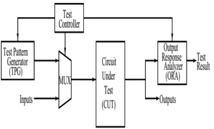
BIST is a design-for-testability technique that places the testing functions physically with the circuit under test (CUT), The basic BIST architecture requires the addition of three hardware blocks to a digital circuit: a test pattern generator, a response analyzer, and a test controller. The test pattern generator generates the test patterns for the CUT. Examples of pattern generators are a ROM with stored patterns, a counter, and a linear feedback shift register (LFSR). A typical response analyzer is a comparator with stored responses or an LFSR used as a signature analyzer. It compacts and analyzes the test responses to determine correctness of the CUT. A test control block is necessary to activate the test and analyze the responses. However, in general, several test-related functions can be executed through a test controller circuit.
. In normal operation, the CUT receives its inputs from other modules and performs the function for which it was designed. During test mode, a test pattern generator circuit applies a sequence of test patterns to the CUT, responses are evaluated by a output response compactor. In the most common type of BIST, test responses are compacted in output response compactor to form (fault) signatures. The response signatures are compared with reference golden signatures generated or stored onchip, and the error signal indicates whether chip is good or faulty.
III. PROPOSED SYSTEM
Control data delivery
The approach summarized in Section II does not make any specific provisions for the way control data is delivered to SoC test logic in order to setup test configurations. Consequently, we begin this paper by analyzing three alternative schemes that can be used to upload control bits and show how they determine the final SoC test logic architecture. A. Using IJTAG The IEEE 1687 is a proposed standard for accessing on-chip test and debug features via the IEEE 1149.1 test access port (TAP). The purpose of this internal Joint Test Action Group (IJTAG) standard is to automate the way one can manage on-chip instruments, and to describe a language for communicating with them via the IEEE 1149.1 test data registers (TDRs). If there is an IJTAG network available on the SoC, and the total number of test configurations is relatively small, one can use it to deliver the control data, as shown in Fig. 3. The SoC design of Fig. 3 has a single TAP and three different blocks: 1) two cores (C1 and C2) under test and 2) the DSR interfacing ATE withC1 and C2. TAP can be instructed to enable a test path via the IEEE 1687 segment insertion bits (SIBs). Every SIB is used to either enable or disable the inclusion of an instrument into the path from a test data In to a test data output. The TDR in C1 orC2 can be either bypassed or loaded with data putting both cores into specific test modes. The TDR in DSR receives the control data indicating which core and which of its test channels are connected to which ATE channels.
ISSN(Online): 2319-8753 ISSN (Print): 2347-6710
I
nternational
J
ournal of
I
nnovative
R
esearch in
S
cience,
E
ngineering and
T
echnology
(A High Impact Factor & UGC Approved Journal)
Website: www.ijirset.com
Vol. 6, Issue 8, August 2017
Fig.4. Dedicated control chain-based architecture.
The advantage of using the IJTAG network to deliver the DSR control data is a simple and easy way to implement flow as the network is frequently used to set the cores TDRs. However, such an approach can only support a limited number of configurations. This is because the IJTAG shift clock is typically 10 to 20 times slower than the scan shift clock. Delivering a large volume of control data can incur an unacceptable total test time overhead. Consequently, this architecture can be used for a relatively small number of test configurations. If the TDRs work with parallel update registers and many patterns use the same configuration, a low throughput IJTAG control can be mitigated. If one changes the control state rather seldom, the next configuration vector can be shifted in coincidently with application of test patterns, followed by updating TDR when ready to switch to the new configuration. It requires more DFT logic, though.
Test Control Architectures
In this section, we first introduce the basic network components. Then we present three proposed test control architectures.
Network Components
ISSN(Online): 2319-8753 ISSN (Print): 2347-6710
I
nternational
J
ournal of
I
nnovative
R
esearch in
S
cience,
E
ngineering and
T
echnology
(A High Impact Factor & UGC Approved Journal)
Website: www.ijirset.com
Vol. 6, Issue 8, August 2017
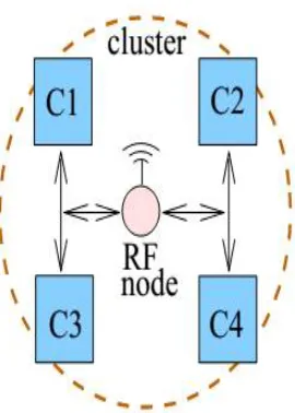
Figure 5: A RF node in a cluster of cores.
Miniature Wireless LAN Based Test Control Network
Our first proposal is a miniature wireless LAN (local area network) that works as the intra-chip test control network for system-chips, where the scheduler broadcasts control signals through the attached RF node as shown in Figure 2. A single wireless channel is shared by all RF nodes in the chip and the control signals sent from the scheduler will be received by all RF nodes. Each RF node has a unique ID and each control signal is attached with an ID field to specify the intended recipient. Upon receiving a signal, a node checks the ID field through its local decoder. If the signal is intended for the receiving node, the node processes the control signal otherwise, it is just ignored. By specifically assigning the ID (for example, reserving one bit to indicate multicasting while the remaining bits are to hold a group number), we can also support multicasting to a subset of RF nodes and consequently a subset of cores can be tested concurrently
ISSN(Online): 2319-8753 ISSN (Print): 2347-6710
I
nternational
J
ournal of
I
nnovative
R
esearch in
S
cience,
E
ngineering and
T
echnology
(A High Impact Factor & UGC Approved Journal)
Website: www.ijirset.com
Vol. 6, Issue 8, August 2017
Using Pipelines
Fig. 6. Pipeline architecture.
One can also use the regular scan channels to deliver controls through pipelining stages, as shown in Fig. 7. For each channel, this approach concatenates control bits, wherein and mare the numbers of control bits used by the in demultiplexers and output multiplexers, respectively. Moreover, each control bit is shadowed to avoid distorting test configurations in the middle of test data shifting. The shadow registers are updated at the end of each pattern upload. Thus, when a test pattern launches a new test configuration, the corresponding control data need to be loaded with its predecessor. Clearly, the first vector is exclusively a setup one. The architecture of Fig.6 supports as many test configurations as required. However, the control data is always uploaded through the ATE channels as an integral part of a test vector. Hence, given a test configuration, the same control data is repeated for all test patterns. The amount of control data is small, though, as the number of control bits per channel is typically a tiny fraction of the test pattern shift cycles.
IV. CONCLUSION AND FUTURE WORK
In this paper, we have proposed a novel distributed wireless test control network using the “radio-on-chip” technology for future high density, high volume embedded system chips. Three types of control architectures, i.e., miniature WLAN, multichip scheme and distributed multichip scheme have been presented and the system optimization has been performed on control constrained test resource partitioning and distribution. In future research, several system optimization issues such as RF nodes placement, the optimal number of RF nodes and routing problems will be addressed in detail under the multilevel tree structure. Simulations using randomly generated test sets and experiments with benchmarks will be performed for evaluation and verification of the proposed test optimization algorithms.
ISSN(Online): 2319-8753 ISSN (Print): 2347-6710
I
nternational
J
ournal of
I
nnovative
R
esearch in
S
cience,
E
ngineering and
T
echnology
(A High Impact Factor & UGC Approved Journal)
Website: www.ijirset.com
Vol. 6, Issue 8, August 2017
Proposed System: Pipelined Architecture:
Dedicated
Design summary:
Existing:
ISSN(Online): 2319-8753 ISSN (Print): 2347-6710
I
nternational
J
ournal of
I
nnovative
R
esearch in
S
cience,
E
ngineering and
T
echnology
(A High Impact Factor & UGC Approved Journal)
Website: www.ijirset.com
Vol. 6, Issue 8, August 2017
Dedicated
REFERENCES
[1] K. Chakrabarty, “Test scheduling for core-based systems using mixedinteger linear programming,” IEEE Trans. Comput.-Aided Design Integr. Circuits Syst., vol. 19, no. 10, pp. 1163–1174, Oct. 2000.
[2] K. Chakrabarty, V. Iyengar, and M. D. Krasniewski, “Test planning for modular testing of hierarchical SOCs,” IEEE Trans. Comput.-Aided Design Integr. Circuits Syst., vol. 24, no. 3, pp. 435–448, Mar. 2005.
[3] A. Chandra and K. Chakrabarty,“A unified approach to reduce SOC test data volume, scan power and testing time,”IEEE Trans. Comput.-Aided Design Integr. Circuits Syst., vol. 22, no. 3, pp. 352–362, Mar. 2003.
[4] S. K. Goel and E. J. Marinissen, “Effective and efficient test architecture design for SOCs,” inProc. Int. Test Conf. (ITC), 2002, pp. 529–538. [5] S. K. Goel, E. J. Marinissen, A. Sehgal, and K. Chakrabarty, “Testing of SoCs with hierarchical cores: Common fallacies, test access optimization, and test scheduling,”IEEE Trans. Comput., vol. 58, no. 3, pp. 409–423, Mar. 2009.
[6] P. T. Gonciari and B. M. Al-Hashimi, “A compression-driven test access mechanism design approach,” inProc. 9th IEEE Eur. Test Symp. (ETS), May 2004, pp. 100–105.
[7] Y. Huang et al., “Optimal core wrapper width selection and SOC test scheduling based on 3-D bin packing algorithm,” inProc. Int. Test Conf. (ITC), 2002, pp. 74–82.
[8] V. Iyengar and K. Chakrabarty, “System-on-a-chip test scheduling with precedence relationships, preemption, and power constraints,” IEEE Trans. Comput.-Aided Design Integr. Circuits Syst., vol. 21, no. 9, pp. 1088–1094, Sep. 2002.
[9] V. Iyengar, K. Chakrabarty, and E. J. Marinissen, “Test wrapper and test access mechanism co-optimization for system-on chip,” J. Electron. Test., Theory Appl., vol. 18, pp. 213–230, Apr. 2002.
[10] V. Iyengar, K. Chakrabarty, and E. J. Marinissen, “Efficient test access mechanism optimization for system-on-chip,”IEEE Trans. Comput.-Aided Design Integr. Circuits Syst., vol. 22, no. 5, pp. 635–643, May 2003.
[11] V. Iyengar, K. Chakrabarty, and E. J. Marinissen, “Test access mechanism optimization, test scheduling,and tester data volume reduction for system-on-chip,”IEEE Trans. Comput., vol. 52, no. 12, pp. 1619–1632,Dec. 2003.
[12] V. Iyengar, A. Chandra, S. Schweizer, and K. Chakrabarty, “A unified approach for SoC testing using test data compression and TAM optimization,” inProc. Des., Autom. Test Eur. Conf. Exhibit. (DATE), 2003,
pp. 1188–1189.
[13] J. Janicki, M. Kassab, G. Mrugalski, N. Mukherjee, J. Rajski, and J. Tyszer, “EDT bandwidth management in SoC designs,” IEEE Trans. Comput.-Aided Design Integr. Circuits Syst., vol. 31, no. 12,
pp. 1894–1907, Dec. 2012. [14] J. Janicki, G. Mrugalski, J. Rajski, and J. Tyszer, “Bandwidth-aware test compression logic for SoC designs,” inProc. 17th IEEE Eur. Test Symp. (ETS), May 2012, pp. 14–19.