International Journal of Research (IJR) Vol-1, Issue-10 November 2014 ISSN 2348-6848
Serial Communication Protocol
Manshi Bisht, Lakshmi rajput, Nikhil kumar
Dept. of Electronics& Communication EngineeringDronacharya College of Engg. Farruhknagar , Gurgaon, India
Abstract
The Hard Core Processor (Power PC) can be replaced by Sot Core Processor (Micro Blaze) to develop SoC based applications on FPGA and this also reduces the cost o IP Cores. But the existing problem with Micro Blaze Soft Core Processor is that it does not have capability to read data from high speed sensors. Due to this the usage of Micro Blaze is limited to low frequency I/O applications. By introducing a high speed serial communication protocol this problem can be eliminated without increasing the hardware resources. This high speed serial communication protocol based on FPGA or SoC applications is proposed in this paper. The design is adopted Spartran 3E FPGA chip and simulation results indicate that it satisfies protocol requirements.
Keywords–
Micro Blaze; FPGA; Serial Communication; Serial to Parallel Conversion; Parallel to Serial Conversion
I. INTRODUCTION
As in SoC applications if IP core is soft core processor such as Micro blaze, it does not have capability to interface with high speed I/O devices due to which the usage is limited to low frequency applications even though the clock of Micro blaze is of high frequency. Sometimes the Micro blaze has to cross link with the devices which are on-chip for data acquisition and data processing. By introducing a standard serial communication protocol the data rate can be
greatly increased and Micro blaze can access data from high speed I/O devices.
Serial communication is used for all long-haul communication and most computer networks, where the cost of cable and synchronization difficulties make parallel communication impractical. Serial computer buses are becoming more common even at shorter distances, as improved signal integrity and transmission speeds in newer serial technologies have begun to outweigh the parallel bus's advantage of simplicity (no need for serializer and deserializer, or SerDes) and to outstrip its disadvantages (clock skew, interconnect density). The migration from PCI to PCI Express is an example.
Micro blaze is a soft core processor, the part of the FPGA will acts as a Micro blaze processor by implementing the hardware description language. In Hard core processor such as Power PC, the memory cannot be varied depending on requirement, which is possible in the case of Micro blaze soft core processor. Another advantage is no need of any external usage of hardware resources to develop IP core which reduces the cost of IP core.
International Journal of Research (IJR) Vol-1, Issue-10 November 2014 ISSN 2348-6848
II. FPGA & HDL
FPGA is a general purpose user programmable device. FPGA demonstrates good performance and logic capacity by exploiting parallelism. At present single FPGA platform can play multi-functions, including control, filter and system. FPGA design flow is a three-step process consisting of design entry, implementation, and verification stages. The full design flow is an iterative process of entering, implementing, and verifying the design until it is correct and complete. The key advantage of HDL when used for systems design is that it allows the behavior of the required system to be described (modeled) and verified (simulated) before Synthesis tools translate the design into real hardware (gates and wires). HDL describes hardware behavior. There are main differences between traditional programming languages and HDL. Traditional languages are a sequential process whereas HDL is a parallel process. HDL runs forever whereas traditional programming language will only run if directed.
FPGA consists of Programmable logic unit, the wiring resources and I/O unit which are programmable. FPGA is suitable mainly for complex designs. The design of FPGA is flexible. The logic blocks, routing resources and I/O unit can be programmed by the user to realize any logic function and to meet various requirements.
III. DESIGN STRUCTURE
A) Serial Communication Protocol
The CLK signal is main clock signal coming from the Micro Blaze soft core processor with 50 MHz frequency or with 20ns period. This CLK is treated as serial clock signal. This CLK is divided by 128 to produce
CLK_DIV signal which is treated as parallel clock. The parallel clock period is 2560ns. DI and TX are the data signals, parallel and serial data respectively. STB is the strobe signal which goes low when parallel data is converted into serial data. After completion of parallel to serial conversion, STB signal goes high. The STB signal goes low for a period of 640ns. This STB signal indicates data sending is finished.
This interface control logic is located on data processing module, FPGA communicates with Micro Blaze processor by internal bus. FPGA adopts the Xilinx Company’s Spartan3e series, the input signal includes 50MHz clock, data/address multiplexing bus and write enabling signals. The output signal is CLK, STB, DI which are the signal the protocol requires.
The Micro Blaze processor sends 8 bits of data in the form of cmds through RS232 cable. In this paper, 4 cmds are combined to give 32 bit of data. This data is processed and will be converted into serial data based on this communication protocol.
Figure 1: Whole Protocol
B) Block Diagram
International Journal of Research (IJR) Vol-1, Issue-10 November 2014 ISSN 2348-6848
unit. The data buffer unit is nothing but RAM which can store 32 bit of data. Whenever required the data can be read from the data buffer unit and is given to the parallel to serial converter. The parallel to serial converter consists of PISO shift register. The total protocol is based on the clock signals which are generated by the clock generating unit. To view the output in PC serial to parallel converter is used which converts serial data to parallel data.
Figure 2: Block Diagram
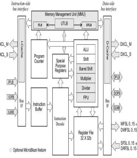
IV. MICRO BLAZE SOFT CORE PROCESSOR
Micro blaze is a soft core processor. A part of the FPGA will acts as a Micro blaze processor by implementing IP core in hardware description language. In Hard core processor such as Power PC the memory cannot be varied depending on requirement, which is possible in the case of Micro blaze soft core processor. Another advantage is no need of any external usage of hardware resources to develop IP core which reduces the cost of IP core.
The Micro blaze embedded processor soft core is a reduced instruction set computer (RISC) optimized for implementation in Xilinx FPGAs. It is highly configurable, allowing users to select a specific set of
functionality required by designs to build their own hardware platform. Fast Simplex Link (FSL) bus is a uni-directional point-to-point channel bus used to perform fast communication between any two design elements on the FPGA when implementing an interface to the FSL bus.
Figure 3: Micro Blaze Soft Core Processor
In Xilinx, Embedded Development Kit (EDK) is used to develop embedded processor by using Base System Builder. The memory type and size can be defined by the user depending on the requirement and the netlist can be generated. Then System Development Kit (SDK) can be used to program the processor using C/C++.
V. REALIZATION OF MODULES
The interface logic mainly includes four function modules:
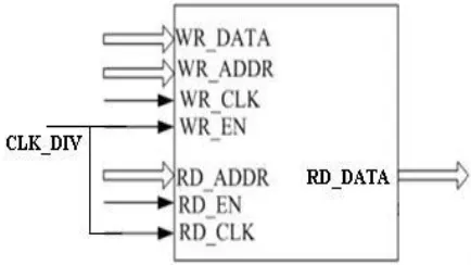
1. Data Buffer Unit:
International Journal of Research (IJR) Vol-1, Issue-10 November 2014 ISSN 2348-6848
data in buffer to parallel to serial conversion unit to process.
Figure 4: Data Buffer Unit
This module’s input signal includes write enabling (WR_EN), read enabling (RD_EN), write clock (WR_CLK), read clock (RD_CLK), write address (WR_ADDR), read address (RD_ADDR) and write data (WR_DATA), Output port uses synchronized output RD_DATA. After the power is reset, if WR_EN is effective, then data is wrote to WR_ADDR corresponding data unit under the action of the WR_CLK clock edge; if WR_EN is ineffective, then write port is closed. When RD_EN is effective, the data in RD_ADDR address space is read under the action of the RD_CLK clock edge as the initial data in the parallel to serial conversion unit.
2. Clock Generating Unit:
The clock generating unit is the functional unit that is mainly responsible for generating various required clock signal according to protocol requirements; input is the interval bus clock signal which Micro blaze output; frequency is 50MHz; at the same time it provides sampling basic clock for parallel to serial conversion unit and generates sending finish signal STB (serial_en signal).
Figure 5: Clock Generating Unit
The Clock Generating Unit is responsible for generating required clock pulses which will satisfy the protocol. The Frequency Divider can be developed by using a 7 – bit counter. This counter produces CLK_DIV whose cycle period is equal to the 128 cycle’s period of CLK. As CLK signal frequency is 50 MHz and period is 20ns. This is the main clock signal coming from Micro Blaze. This acts as clock signal to the 7 – bit counter. The counter counts this clock signal and produces its output. Based on the proper HDL code the clock signal will be divided into CLK_DIV signal whose frequency is approximately 3.9 KHz and period is 2560ns. This CLK_DIV along with CLK signal acts as clock signal to Parallel to Serial Conversion Unit. The realization of code is as follows:
process(rst,clk)
variabletemp:std_logic_vector(6 downto 0); begin
ifrst='1' then temp:="0000000";
elsifclk'event and clk='1' then temp:=temp+1;
end if;
clk_div1<=temp(temp'high); end process;
International Journal of Research (IJR) Vol-1, Issue-10 November 2014 ISSN 2348-6848
3. Parallel to Serial Conversion Unit:
The parallel to serial conversion unit is the functional unit that is mainly responsible for the conversion of parallel data is to serial data; the data is output on the CLK clock edge according to protocol requirements. After the module are electrified, firstly the data which will be sent is wrote in data buffer unit; then the module receives upper software order to send data; the data buffer unit sends the data to parallel to serial conversion unit to data transform and produces serial DI data; After waiting serial data ready, clock generating unit produces CLK signal according to protocol requirements and produces STB signal after data sending has been finished for some time , this data sending has been finished.
4. Serial to Parallel Conversion Unit:
This unit is used to convert the serial input into the form of parallel. This final parallel data will be again sent to the Micro blaze to see the output in terminal in pc through RS232 cable.
Serial to Parallel Conversion can be carried out based on CLK signal. A SIPO Shift Register can be used to develop Serial to Parallel Converter. SIPO register receives data in serial form and outputs data to Micro Blaze in parallel form. This parallel data is given to Micro Blaze to view output using Terminal Software. The realization of code is as follows:
process(sclk,serial_en) begin
ifsclk'event and sclk='0' and serial_en='0' then
parallel_data_sig<= serial data ¶llel_data_sig(31 downto 1);
end if; end process; process(serial_en) begin
--if count="00000" and serial_en /='0' then
ifserial_en ='1' then
parallel_data<= parallel_data_sig; else
parallel_data<=(others=>'0'); end if;
end process;
VI. EMULATION RESULTS
The emulation result shows that the serial clock’s frequency is higher than the parallel clock’s frequency. During the parallel to serial conversion, the strobe signal goes low. After the conversion, the strobe signal goes high. It will retain in high state until another data is given for conversion.
The given input is 92345673 and its binary
equivalent is
“10010010001101000101011001110011”. The MSB indicates the start of the data and it should be kept at high to convert data into serial form.
International Journal of Research (IJR) Vol-1, Issue-10 November 2014 ISSN 2348-6848
VII. CONCLUSION
As the Micro blaze processor is limited to low frequency applications, introduction of private serial communication protocol increases data transmission rate without increasing the hardware resources. In this paper the serial communication protocol for FPGA based SoC applications is shown, which reduces the development cycle, reduces the man power investment and increases reliability. The same FPGA can be used for developing Micro blaze and the protocol, this design reduces the cost and this design is worth promoting in future scope.
REFERENCES
[1] Design of Serial Communication Interface Based on FPGA PengHui-ling; NieYa-lin; Dept. of Comput. & Inf. Eng., Luoyang Inst. of Sci. & Technol., Luoyang, China
[2] Computer Science and Automation Engineering (CSAE), 2011 IEEE International Conference
[3] LIU Wan, HE Dao-jun, TAN Ming. The Design and Application of FPGA. Beijing: Tsinghua University Press, China, June 2006.
[4] GuoShu-tao, JING Yong-zhi.Serial Communication Based on FPGA. The transaction of Beijing Electronic Science and Technology Institute , China, Vol .14,No.4,December2006 [5] JIANG Wei, WANG Kai-jun,
CHEN Han-mei. A Design of Serial Communication Based on FPGA. Journal of Engineering Design, China, Vol.10, No. 2, April 2003.
[6] ZHANG Yi. MCS51