Article
1
Thermoelectric properties of Bi
2Te
3: CuI and the effect
2
of its doping with Pb atoms
3
Mi-Kyung Han1, Yingshi Jin1, Da-hee Lee1, and Sung-Jin Kim1,*
4
1 Department of Chemistry and Nano Science, Ewha Womans University, Seoul 120-750, Korea
5
6
* Correspondence: [email protected]; Tel.: +82-2-3277-4164
7
Abstract: In order to understand the effect of Pb-CuI co-doping on the thermoelectric performance
8
of Bi2Te3, n-type Bi2Te3 co-doped with x at% CuI and 1/2x at% Pb (x = 0, 0.01, 0.03, 0.05, 0.07, and
9
0.10) were prepared via high temperature solid state reaction and consolidated using spark plasma
10
sintering. Electron and thermal transport properties, i.e., electrical conductivity, carrier
11
concentration, Hall mobility, Seebeck coefficient, and thermal conductivity, of CuI-Pb co-doped
12
Bi2Te3 were measured in the temperature range from 300 K to 523 K and compared to
13
corresponding x% of CuI-doped Bi2Te3 and undoped Bi2Te3. The addition of a small amount of Pb
14
significantly decreased the carrier concentration, which could be attributed to the holes from Pb
15
atoms, thus the CuI-Pb co-doped samples show a lower electrical conductivity and a higher
16
Seebeck coefficient compared to CuI-doped samples with similar x values. The incorporation of Pb
17
into CuI-doped Bi2Te3 rarely changed the power factor because of the trade-off relationship
18
between the electrical conductivity and the Seebeck coefficient. The total thermal conductivity(κtot)
19
of co-doped samples (κtot ~1.4 W/m∙K at 300 K) is slightly lower than that of 1% CuI-doped Bi2Te3
20
(κtot~1.5 W/m∙K at 300 K) and undoped Bi2Te3 (κtot ~1.6 W/m∙K at 300 K) due to the alloy scattering.
21
The 1% CuI-Pb co-doped Bi2Te3 sample shows the highest ZT value of 0.96 at 370 K. All data on
22
electrical and thermal transport properties suggest that the thermoelectric properties of Bi2Te3 and
23
its operating temperature can be controlled by co-doping.
24
Keywords: Bi2Te3, Thermoelectric properties, doping
25
26
27
1. Introduction
28
Bismuth telluride (Bi2Te3) has been the focus of extensive theoretical and experimental studies
29
as a component of materials for thermoelectric (TE) devices, such as solid-state coolers or
30
generators.[1-3] The performance of a thermoelectric material in the aforementioned applications is
31
evaluated in terms of a dimensionless figure of merit ZT, which is defined as (S2
σ
/κ)T; where S is the32
Seebeck coefficient (or thermopower),
σ
is the electrical conductivity, κ is the thermal conductivity,33
and T is the temperature.[4] The product (S2
σ
) is called the power factor. A larger ZT directly leads to34
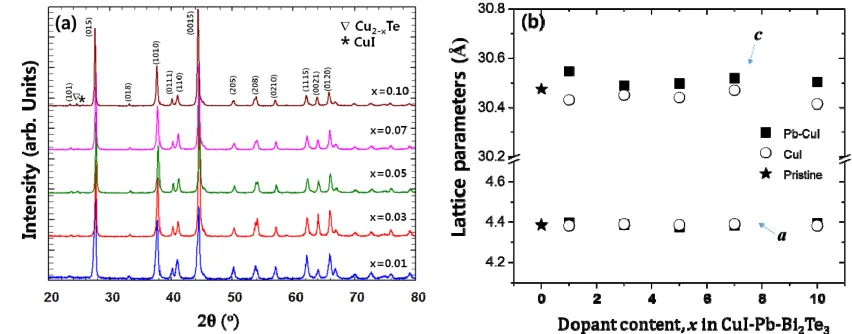
a higher conversion efficiency. The main challenge lies in the decoupling of the interdependent
35
thermoelectric parameters (S,
σ
, and κ), which are strongly coupled to the carrier concentration.36
Commercial TE devices comprise series of p- and n-type semiconductor pairs.
37
The ZT values of commercial Bi2Te3 compounds are about 1.35 for p-type and 0.9 for n-type
38
materials.[5] The poor performance of n-type Bi2Te3 based materials compared to that of p-type
39
materials seriously inflicts a limitation on making it a more efficient TE device. Both p-type and
40
n-type characteristics of Bi2Te3 can be controlled depending on the chemical composition. As is well
41
known, n-type Bi2Te3 have been synthesized by making solid solution with Bi2Se3 or addition of
42
excess tellurium as an electron donor.[6,7] However, the fabrication of n-type Bi2Te3 thermoelectric
43
materials has a number of technical problems, such as controlling the Se content in Bi2Te3-Bi2Se3 solid
44
solution is difficult and Te-rich Bi2Te3 easily decompose upon heating. Element doping is a more
45
effective approach to enhance the thermoelectric properties of Bi2Te3-based alloys.[8-12] Among
46
various dopant, Cu or Cu-halide acts as an excellent additive for improvement of thermoelectric
47
performance of n-type Bi2Te3.[13-16] Cu atoms can be either an acceptor or a donor depending on their
48
location in the compound. Cu is also known to improve the reproducibility of thermoelectric materials,
49
due to the formation of Cu–Te bond in the van der Waals gaps which suppress the escape of Te atoms.[17]
50
The Cu-intercalated Bi2Te3 bulk shows a significantly enhanced ZT of ~1.12 at 300 K,[13]which is the
51
highest ZT value reported for n-type Bi2Te3 binary material. Cu addition can also prevent the
52
oxidation of the Bi2Te3.[17]However, the thermoelectric properties of these alloys change with aging
53
time.[18] Studies of the structure and properties of crystals with a co-dopant with Cu content were
54
carried out.[16, 19, 20]Cu and I atoms co-doped Bi2Te3 was prepared using the Bridgman method for
55
the improvement of its corresponding thermoelectric properties, whereby the power factor was
56
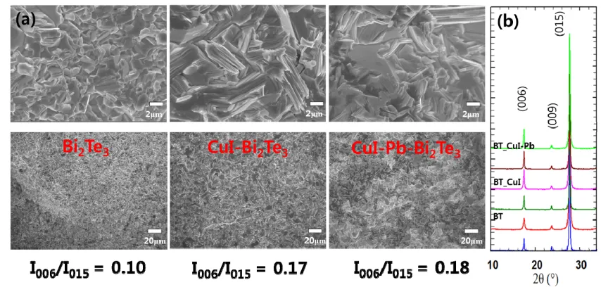
improved through the co-doping effect of Cu and I, while its thermal conductivity was reduced by
57
forming dispersed Cu-rich nanoprecipitates. The maximum ZT of ~ 1.16 was achieved at a
58
temperature of 368 K for (CuI)0.01Bi2Te3.[16] Moreover, various dopants (Au, Mn, Co, Ni, Zn, Ge, Ag,
59
In, Sc, Ti, V, and Sn) in Cu0.008Bi2Te2.7Se0.3 have been studied.[19,20] The addition of dopant atoms at Bi
60
sites in n-type Cu-intercalated Bi2Te3 changes the electronic band structure, such as band position
61
and band degeneracies, resulting in an increase of the Seebeck coefficient. As a consequence, peak
62
ZT values of 0.88 at 360 K and 0.91 at 320 K were obtained for V-doped and Au-doped
63
Cu0.008Bi1.98Te2.7Se0.3, respectively.[19, 20]Therefore, it has great potential to further improve the ZT
64
value of n-type Bi2Te3 based materials via compositional tuning approach by adjusting Cu contents
65
or element doping.
66
In the present study, CuI-Pb co-doped Bi2Te3 samples were prepared using high temperature
67
solid state reaction method and consolidated by SPS. The Pb-addition effects on the crystal lattice,
68
the charge transport, and the thermoelectric properties of CuI-doped Bi2Te3 were evaluated.
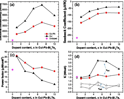
69
2. Results and Discussion
70
Powder X-ray diffraction (PXRD) patterns of x% CuI-Pb co-doped Bi2Te3 (x = 0.01, 0.03, 0.05, 0.07,
71
and 0.10) samples are shown in Figure 1(a). As a comparison, undoped Bi2Te3 and x% CuI-doped
72
Bi2Te3 were prepared under the same synthetic conditions. All of the diffraction peaks are indexed to
73
rhombohedral Bi2Te3 structure with the space group of R m (JCPDS, No. 15-0863),[23] with no
74
indication for the existence of a second phase for samples with up to 7% of dopant concentration.
75
Trace amounts of possible impurities including Cu2-xTe and CuI were detected in the 10% CuI-Pb
76
co-doped Bi2Te3 samples. This result implies that the solubility limit of CuI and Pb dopants in Bi2Te3
77
was x < 0.1. While in previous report, the impurity phase was observed in less than 5% in CuI-doped
78
Bi2Te3 sample[16], when Pb atoms are co-doped with CuI in Bi2Te3, the impurity phase was observed
79
only in a 10% CuI-Pb co-doped Bi2Te3 sample. This result indicates that the solubility of CuI in Bi2Te3
80
is increased by addition of Pb atoms. Figure 1(b) shows the lattice parameters of CuI-Pb co-doped
81
and CuI-doped Bi2Te3 samples as a function of the dopant fraction. In all samples, the in-plane
82
parameter a remains constant, while the unit cell parameter c along the stacking direction expands
83
with increasing Pb content in the CuI-Bi2Te3 system. The result is presumably a consequence of Cu
84
atoms entering into the interstitial site, which increases the distance between the van der Waals
85
layers.[13] A comparison of the covalent radius of Pb (rPb = 0.147 nm) with that of Bi (rBi = 0.146 nm)
86
shows that the size of Pb is very close to that of Bi and thus the ability of Pb atoms for the
87
substitution of Bi atoms in Bi2Te3 should not be neglected. Halogen atoms such as I (rI = 0.220 nm) are
88
believed to occupy Te (rTe = 0.221 nm) sites in the lattice.[24] The incorporation of iodine atoms to Te
89
sites and Pb atoms to Bi sites drive the changes in bonding parameters. The substituted atoms bridge
90
scope of this paper and would demand quantum chemical calculations of bonding parameters,
92
which will be the aim of our next work.
93
94
Figure 1. (a) Powder X-ray diffraction patterns of samples of x% CuI-Pb co-doped Bi2Te3 (x = 0.01,
95
0.03, 0.05, 0.07, and 0.10) with peaks of impurity phases (marked by symbols (∇ and *)), (b) Lattice
96
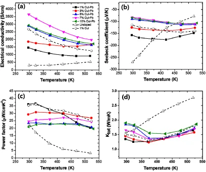
parameters of samples of x% CuI-Pb co-doped Bi2Te3 (x = 0, 0.01, 0.03, 0.05, 0.07, and 0.10)
97
98
In our previous work, we demonstrated that doping of Bi2Te3 samples with 1% CuI enhanced
99
ZT.[16] Thus we selected 1% CuI-doped Bi2Te3 sample as a reference material to demonstrate the
100
effect of CuI-Pb co-doping on the charge transport properties. The charge transport properties of 1%
101
CuI-Pd co-doping Bi2Te3 at room temperature are investigated by Hall effect analysis and compared
102
to those of 1% CuI-doped Bi2Te3 and undoped Bi2Te3. Assuming one carrier type and parabolic bands
103
in our analysis, the carrier concentration (n) was calculated from the room temperature (i.e., well
104
within a single-carrier dominated transport) Hall constants using the relationship RH = 1/ne, where
105
RH is the Hall coefficient, n is the carrier concentration, and e is the electronic charge. The Hall
106
coefficients of specimens are negative, indicating n-type conductions. By incorporating Pb in CuI-
107
Bi2Te3 system, the ne value of the bulk samples decreases from ~ 7.8 × 10¹⁹ /cm3 (CuI-doped Bi2Te3) to
108
~3.6 × 10¹⁹ /cm3 (CuI-Pb co-doped Bi2Te3) and the corresponding mobility value increases from ~
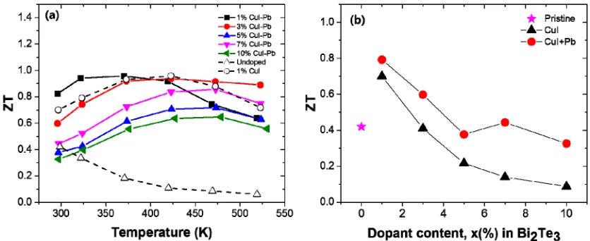
109
164.6 cm2/V∙s to ~ 216.9 cm2/V∙s at 300 K. In comparison, the undoped Bi2Te3 sample shows the n
110
value of ~ 1.2 × 10¹⁹ /cm3and the mobility of 354.9 cm2/V∙s at 300K. This result verifies that the
111
addition of a small amount of Pb significantly decreases the carrier concentration, which should be
112
attributed to the holes generated by the Pb atoms. This demonstrates that facile control of electron
113
concentration can be easily realized by adding Pb atoms to CuI-doped Bi2Te3 system, yielding an
114
optimal electron concentration of 3-4.5 × 10¹⁹ /cm3.
115
Figure 2(a) shows SEM images of the fractured surfaces of SPSed undoped Bi2Te3, 1% CuI-doped
116
Bi2Te3, and 1% CuI-Pb co-doped Bi2Te3. All samples exhibit lamellar structures at the micron scale
117
and no obvious large-scale preferred orientation. The microstructures are dense (> 98% of the
118
theoretical density of n-type Bi2Te3 (7.86 g/cm3) showing densities of 7.73 g/cm3, 7.77 g/cm3 and 7.82
119
g/cm3 for undoped Bi2Te3, 1% CuI-doped Bi2Te3, and 1% CuI-Pb co-doped Bi2Te3, respectively. The
120
this method, F is expressed as the following equations: F = P − P0/1 − P0, P0 = I0(0 0 l)/∑I0(hkl),
122
P = I(0 0 l)/∑I(hkl), where I0(0 0 l) is the intensity of (0 0 l) peaks and ∑I0(hkl) is the sum of intensities of all
123
peaks for the powders with random orientation; I(0 0 l) is the (0 0 l) peak intensity and ∑I(hkl) is the sum
124
of the intensities of all peaks for the measured section. We calculated the ratios I(0015)/I(015) of the
125
integrated intensity of (0015) to (015) and represented them in Figure 2(b) to evaluate the grain
126
orientation anisotropy. All samples show anisotropy in the crystal structure; however, the degree of
127
anisotropic orientation is not significant in SPS consolidated polycrystalline samples. The I(0015)/I(015)
128
value for 1% CuI-doped Bi2Te3 and 1% CuI-Pb co-doped Bi2Te3 (17%–18%) is slightly higher than
129
those for undoped Bi2Te3 (10%). This indicates that the c-axis of the grains after SPS was
130
preferentially oriented parallel to the pressing direction. This result is consistent with a previous
131
report[16], showing the strengthening of the two adjacent quintuple layers by substituting Te with I
132
atoms. Effect caused by sample density or sample orientation are negligible since the relative
133
densities and orientation degree determined by the Lotgering method for CuI-doped and CuI-Pb
134
co-doped Bi2Te3 samples are nearly same.
135
136
137
Figure 2.(a) SEM images, and (b) XRD patterns of undoped Bi2Te3, 1% CuI-doped Bi2Te3, and 1%
138
CuI-Pb co-doped Bi2Te3.
139
140
The thermoelectric properties depend on the dopants (here we use CuI only and CuI-Pb),
141
dopant content, and temperature. In order to elucidate the effect of dopants and their contents on the
142
thermoelectric properties, the dependence of the electrical conductivity (
σ
), Seebeck coefficient (S),143
and power factor on dopant concentration x in the CuI-doped and CuI-Pb co-doped Bi2Te3 (x = 0, 0.01,
144
0.03, 0.05, 0.07, and 0.10) system was investigated, as shown in Figure 3. In both series, with
145
increasing dopant concentration, the electrical conductivity increase, while the Seebeck coefficient
146
decreases simultaneously for up to 7% of dopant concentration. The room temperature electrical
147
conductivity of the undoped Bi2Te3 (~ 307 S/cm) is increased by CuI-doping (1% of CuI-doped Bi2Te3
148
Bi2Te3 at 300 K was about ~ 1462 S/cm. This value is significantly lower than that of 1% CuI-doped
150
Bi2Te3. As shown in Figure 3(a), the CuI-Pb co-doped samples show a lower electrical conductivity
151
than that of CuI-doped samples with similar x values, confirming the role of Pb as an acceptor.[26] In
152
Figure 3(b), the Seebeck coefficients at room temperature were plotted as a function of dopant
153
contents. The value of Seebeck coefficient at 300 K for CuI-doped and CuI-Pb co-doped Bi2Te3 are
154
about -115 μV/Kand -157 μV/K, respectively, while that for undoped Bi2Te3 is -270 μV/K, which
155
compares well with previous reported value for n-type Bi2Te3.[2] The Seebeck coefficients of the
156
CuI-Pb co-doped bulk samples are observed to be higher than that of the CuI-doped sample due to
157
lower carrier concentrations. Normally Bi2Te3 shows p-type character, however the undoped Bi2Te3
158
in this study show n-type character. We assume that these differences arise from the different doping
159
due to the different experimental conditions used for the preparation of undoped Bi2Te3 crystals. The
160
Bi2Te3 prepared by the Bridgman method is a p-type conductor due to the antisite defectf of BiTe.
161
However, in this work, the SPS pressed Bi2Te3 sample show n-type characteristics, which arises from
162
the Te vacancy at the interface. This decrease in electrical conductivity and the increase in Seebeck
163
coefficient in co-doped samples can be explained by an increased carrier scattering related to the
164
incorporation of Pb atoms in the CuI-doped lattice and by decreased carrier concentrations caused
165
by Pb atoms which act as electron acceptors.[26] As shown in Figure 3(c), the CuI-Pb co-doped
166
samples show higher power factors than CuI-doped samples with similar x values. The power
167
factors decrease with increasing dopant concentrations. The maximum values of the power factors
168
were observed at x = 0.01 for both CuI and CuI-Pb co-doped samples. The benefit of Pb incorporation
169
into CuI-doped Bi2Te3 was not observed in the power factor because of the trade-off relationship
170
between the Seebeck coefficient and the electrical conductivity. ( 35 μW/cm∙K2 for 1% CuI-doped
171
Bi2Te3; 36 μW/cm∙K2 for 1% CuI-Pb co-doped Bi2Te3). This corresponds to an > 80 % enhancement
172
over the typical value of undoped Bi2Te3 (22 μW/cm∙ K2). Figure 3(d) represents thermal
173
conductivities (closed symbols for
κ
tot and open symbols forκ
latt) as a function of dopant content.174
As the dopant concentration increased, the total conductivity of CuI-doped and CuI-Pb co-doped
175
Bi2Te3 increased due to the increase of the electronic contribution. The total thermal conductivity κtot
176
of 1% CuI-Pb co-dopedsamples (κtot ~1.4 W/m∙K at 300 K) is slightly lower than that of 1%
177
CuI-doped Bi2Te3 (κtot ~1.5 W/m∙K at 300 K) and undoped Bi2Te3 (κtot ~1.6 W/m∙K at 300 K) due to
178
alloy scattering. The lattice part (κlatt) of the thermal conductivity can be estimated by subtracting the
179
electronic component (κelec) from the measured total thermal conductivity, κlatt = κtot −
κ
elec. The180
electronic component is given by the Wiedemann-Franz relation, κelec = L
σ
T, where L is the Lorenz181
number. L is taken to be 1 . 5 × 1 0−8 V2/K2 for near-degenerate or degenerate semiconductor.[27,28]
182
The lattice thermal conductivity of 1% CuI-Pb co-doped Bi2Te3 was 0.66 W/m∙K at 300 K. In contrast
183
to the behavior of
κ
tot upon increasing the dopant concentration, κlatt slightly decreased with184
increasing dopant concentration. This result demonstrates clearly that the lattice κlatt is reduced by
185
187
Figure 3. The composition dependence of (a) electrical conductivity (σ), (b) Seebeck coefficient (S),
188
(c) power factor, and (d) thermal conductivity on dopant concentration x in the CuI-doped (black)
189
and CuI-Pb co-doped Bi2Te3 (x = 0, 0.01, 0.03, 0.05, 0.07, and 0.10) system (red).
190
191
Figure 4 shows the electrical transport properties as a function of measured temperature of x%
192
CuI-Pb co-doped Bi2Te3 (x = 0.01, 0.03, 0.05, 0.07, and 0.10), compared with 1% CuI-doped Bi2Te3 and
193
undoped Bi2Te3. For all samples, a monotonic decrease in electrical conductivity with increasing
194
temperature is observed (Figure 4(a)), indicative of heavily degenerated doping. The variation of the
195
Seebeck coefficient is similar to that of the electrical conductivity, shown in Figure 4(b). The Seebeck
196
coefficient is negative in the whole temperature range, indicating that the majority of charge carriers
197
are electrons (n-type). The magnitude of the Seebeck coefficient initially increases and reaches a
198
maximum that is strongly depend on the Pb content x. The onset of intrinsic conduction (the maxima
199
of the curves) in these samples shifts to higher temperature with increasing dopant content. While
200
the x = 0% sample has its maxima at ~300 K, the 1% and 3% sample have their maximum at ~ 425 K,
201
and the x > 5% sample at ~ 525 K. The maximum value of the Seebeck coefficient (~ -176
μ
V/K) was202
observed at x = 0.01 CuI-Pb content at 425 K. Figure 4(c) shows the power factors (S2
σ
) values as a203
function of temperature. In this system, the power factor values for the 1% CuI-Pb co-doped ranged
204
from 36 μW/cm∙K2 at 300 K to 20 μW/cm∙K2 at 523 K. The CuI-Pb co-doped sample with x > 0.03
205
shows a mild temperature dependence. Figure 4d shows the temperature dependence of the total
206
thermal conductivity κtot of the samples. The κtot of all the doped samples firstly decreases due to the
increasing phonon-phonon scattering, and then increases when upon further increase of the testing
208
temperature due to the increase of ambipolar thermal contributions arising from the diffusion of
209
electron-hole pairs with the onset of intrinsic contribution.[29]
210
211
Figure 4. The temperature dependence of (a) electrical conductivity (σ), (b) Seebeck coefficient (S),
212
(c) power factor, and (d) thermal conductivity of x% CuI-Pb co-doped Bi2Te3 (x = 0.01, 0.03, 0.05, 0.07,
213
and 0.10).
214
215
The dimensionless figure of merit ZT of the samples with different dopant concentration (x) are
216
shown in Figure 5(a) as a function of temperature. The magnitude of the ZT initially increases and
217
reaches a maximum that is strongly dependent on the dopant content x. When the temperature is
218
above ~ 400 K, the ZT values decrease due to the appearance of intrinsic excitation at higher
219
temperature. In this experiment, the ZTmax of the 1% CuI-Pb co-doped sample was about 0.96 at 370 K,
220
while the highest value ZTmax was about 0.96 at 422 K for the 1% CuI-doped sample. The
221
incorporation of Pb into CuI-doped Bi2Te3 led to a shift of the peak position of ZTmax to lower
222
temperatures. This result shows that the optimization of the operating temperature can be controlled
223
by co-doping. For practical applications of thermoelectric materials, the ZT values at room
224
temperature are also important.
Figure
5(b) shows the room temperature dimensionless figures of225
merit ZT of the samples as a function of the dopant concentration. The undoped Bi2Te3 sample shows
a low ZT of ~ 0.42 at 300 K due to its very poor electrical properties. The highest ZT of 0.79 and 0.70
227
at 300 K were achieved for the 1% CuI-Pb doped sample and 1% Cu-doped Bi2Te3 sample,
228
respectively, which are both significantly improved when compared with those of the undoped
229
sample. All evidences about electrical and thermal transport properties suggest that the n-type ZT of
230
Bi2Te3 can be enhanced by the incorporation of Pb with CuI dopant. Further improvement in its TE
231
properties can be expected by choosing suitable combination of dopants.
232
233
Figure 5.(a)Temperature dependency, and (b) Dopant content dependency of the dimensionless
234
figure of merit ZT for x% CuI-Pb co-doped Bi2Te3 (x = 0.01, 0.03, 0.05, 0.07, and 0.10), 1% CuI-doped
235
Bi2Te3, and undoped Bi2Te3.
236
237
3. Materials and Methods
238
3.1. Synthesis of bulk ingot and powder processing.
239
n-type Bi2Te3 co-doped with x at% CuI and 1/2 x at% Pb (x = 0, 0.01, 0.03, 0.05, 0.07, and 0.10)
240
were prepared by means of the conventional high-temperature solid-state reaction method, using Bi,
241
Te, CuI and Pb (All 99.999%, from Alfa Aesar) as starting materials. For convenience, the samples are
242
labeled as dopant contents, such as that Bi2Te3 + x CuI + 1/2x Pb with x is labeled as x% CuI-Pb
243
co-doped Bi2Te3. n-type Bi2Te3 doped with x at% CuI alone was prepared under identical
244
experimental conditions for comparison. The corresponding elements were sealed in appropriate
245
ratio in evacuated fused silica tubes (14 mm diameter, 1 mm wall thickness) under a residual
246
pressure of ~10-4 Torr. The sealed tubes were heated to 1000 oC over 12 h and then held at 1000 oC for
247
12 h while rocking the liquid to facilitate a complete mixing of the contents. The tubes were slowly
248
cooled to 800 °C over a period of 12 h and then quenched to room temperature. The cast ingot
249
samples were powdered by ball milling in an Ar-filled glove box and the ground powder was
250
passed through a 53 μm-mesh sieve. To obtain dense bulk samples, spark plasma sintering (SPS)
251
was performed under Ar atmosphere by using SPS machine (SPS-211Lx, Fuji Electronic Industrial
252
Co., LTD, Japan). Typically 12–13 g of the powdered samples were loaded into the graphite die with
253
an inside diameter of 14 mm and heated to 425 oC for 5 min at a heating rate of 100 °C/min and held
254
there for 5 min under an axial pressure of 50 MPa under a vacuum of 1.4 × 10⁻² Torr.
3.2. Characterization of materials.
256
Powder diffraction pattern was obtained with a Rigaku D/MAX X-ray (40 kV and 30
257
mA) diffractometer with CuKα radiation (λ = 1.54056 Å). The lattice parameters were
258
obtained by least squares refinement of data in the 2θ range of 10°∼70° with the assistance
259
of a Rietveld refinement program.[21] The carrier concentration was measured by a Hall
260
measurement system (BIO-PAD, HL5500PC) at room temperature in air. The morphologies
261
and chemical composition of the SPS-sintered samples were investigated via field-emission
262
scanning electron microscopy (FE-SEM, JEOL JSM-5800F).
263
3.3. Characterization of thermoelectric properties.
264
In order to investigate the thermoelectric properties, the sample (~13 g) after SPS were
265
cut into rectangular shapes with dimensions of ~ 3 × 3 × 10 mm3 and a disk-shape of about
266
∼14 mm diameter and 2 mm thickness. The former specimens were subjected to Seebeck
267
coefficient and electrical conductivity measurements (ULVAC-RIKO ZEM-3) and the latter
268
to thermal diffusivity measurements using a NETZSCH LFA 457 MicroFlash™ instrument.
269
The thermoelectric properties of the samples were measured along the direction
270
perpendicular and parallel to the SPS pressing direction. Only results of perpendicular
271
direction measurements are shown in the manuscript. The thermal conductivity κtot can be
272
obtained from the relationship κtot(T)= D(T)∙Cp(T)∙ρ(T), where Cp is the specific heat, D(T)is
273
the thermal diffusivity, and ρ(T) is the density of the sample. Thermal diffusivity and
274
specific heat were determined by the flash diffusivity-heat capacity method with a
275
Pyroceram standard using the method described in detail in the literature.[22] Sample
276
density (ρ(T)) was calculated from the sample’s geometry and mass. Electrical conductivity
277
and Seebeck coefficient were measured simultaneously under Helium atmosphere from
278
room temperature to approximately 550 K. The Seebeck coefficients were measured three
279
times with different temperature gradients between 5 and 15 K at each temperature step.
280
4. Conclusions
281
In this work, utilizing second dopant, we successfully shifted the optimum ZT of an n-type
282
Bi2Te3-based compound towards a lower temperature. This demonstrates that facile control of the
283
electron concentration can be realized by adding Pb atoms to the CuI-doped Bi2Te3 system, yielding
284
an optimal electron concentration of 3-4.5 × 10¹⁹ /cm3. Whereas the change of room temperature
285
power factor as a consequence of Pb addition was not notable, the thermal conductivity decreased
286
with Pb addition due to the alloying scattering. The maximum ZT of 0.96 was obtained at 370 K for
287
1% CuI-Pb co-doped Bi2Te3. In comparison with 1% CuI-doped and undoped Bi2Te3, the ZT of 1%
288
CuI-Pb co-doped Bi2Te3 (ZT ~ 0.79) at room temperature was enhanced by more than 12% and by
289
88%, respectively.
290
Acknowledgments: This research was supported by Nano Material Technology Development Program
291
through the National Research Foundation of Korea (NRF) funded by the Ministry of Education, Science and
292
Technology (NRF-2011-0030147) and by the National Research Foundation of Korea (NRF) Grant funded by the
293
Korean Government (MSIP) (NRF-2015R1A5A1036133).
294
295
References
297
1. Snyder,G. J.; Toberer, E. S. Complex thermoelectric materials, Nat. Mater. 2008, 7, 105-114,
298
DOI:10.1038/nmat2090
299
2. Rowe, D. M. in: CRC Handbook of Thermoelectrics, CRC Press, New York, 1995, ISBN
300
9780849301469
301
3. Goldsmid, H. J. Bismuth telluride and its alloys as materials for thermoelectric generation
302
Materials 2014, 7, 2577-2592, DOI:10.3390/ma7042577
303
4. Bell, L. E. Cooling, heating, generating power, and recovering waste heat with
304
thermoelectric systems, Science 2008, 321, 1457-1461, DOI:10.1126/science.1158899
305
5. Lan, Y. C.; Minnich, A. J.; Chen, G.; Ren, Z. F. Enhancement of thermoelectric
306
figure-of-merit by a bulk nanostructuring approach, Adv. Funct. Mater. 2010, 20, 357-376,
307
DOI:10.1002/adfm.200901512
308
6. Mehta, R. J.; Zhang, Y. L.; Karthik, C.; Singh, B.; Siegel, R. W.; Borca-Tasciuc, T.; Ramanath,
309
G. A. New class of doped nanobulk high-figure-of-merit thermoelectrics by scalable
310
bottom-up assembly, Nat. Mater. 2012, 11, 233-240, DOI:10.1038/nmat3213
311
7. Kim, S. I.; Lee, K. H.; Mun, H. A.; Kim, H. S.; Hwang, S. W.; Roh, J. W.; Yang, D. J.; Shin, W.
312
H.; Li, X. S.; Lee, Y. H.; Snyder, G. J. Dense dislocation arrays embedded in grain
313
boundaries for high-performance bulk thermoelectrics, Science 2015, 348,109-114,
314
DOI:10.1126/science.aaa4166
315
8. Süssmann, H.; Priemuth, A.; Pröhl, U. Doping properties of Pb and Ge in Bi2Te3 and Sb2Te3,
316
Phys. Status Solidi (A) 1984, 82, 561-567, DOI:10.1002/pssa.2210820229
317
9. Svechnikova, T. E.; Konstantinov, P. P.; Alekseeva, G. T. Physical properties of Bi2Te2.85Se0.15
318
single crystals doped with Cu, Cd, In, Ge, S, or Se, Inorg. Mater.2000, 36, 556-560,
319
DOI:10.1007/BF02757952
320
10. Lee, G. E.; Kim, I. H.; Lim, Y. S.; Seo,W. S.; Choi, B. J.; Hwang, C. W. Preparation and
321
thermoelectric properties of doped Bi2Te3-Bi2Se3 solid solutions, J. Electron. Mater. 2014, 43,
322
1650-1655, DOI: 10.1007/s11664-013-2822-6
323
11. Gasenkova, I. V.; Svechnikova, T. E. Structural and transport properties of Sn-doped
324
Bi2Te3-xSex single crystals, Inorg. Mater. 2004, 40, 570-575,
325
DOI:10.1023/B:INMA.0000031988.18749.88
326
12. Wu, F.; Wang, W.; Hu, X.; Tang, M. Thermoelectric properties of I-doped n-type
327
Bi2Te3-based material prepared by hydrothermal and subsequent hot pressing, Prog. Nat.
328
Sci.2017, 27 203-207, DOI:10.1016/j.pnsc.2017.02.009.
329
13. Han, M. -K.; Ahn, K.; Kim, H. J.; Rhyee, J. -S.; Kim, S. -J. Formation of Cu nanoparticles
330
in layered Bi2Te3 and their effect on ZT enhancement, J. Mater. Chem. 2011, 21,
331
11365-11370. DOI:10.1039/C1JM10163C.
332
14. Liu, W. -S.; Zhang, Q.; Lan, Y.; Chen, S.; Yan, X.; Zhang, Q.; Wang, H.; Wang, D.; Chen, G.;
333
Ren, Z. Thermoelectric property studies on Cu-Doped n-type CuxBi2Te2.7Se0.3
334
nanocomposites, Adv. Energy. Mater. 2011, 1, 577-587, DOI:10.1002/aenm.201100149.
335
15. Sie, F. R.; Kuo, C. K.; Hwang, C. S.; Chou, Y. W.; Yeh, C. H.; Lin, Y. L.; Huang, J. Y.
336
Thermoelectric performance of n-type Bi2Te3 /Cu composites fabricated by nanoparticle
337
decoration and spark plasma sintering, J. Electron. Mater. 2016, 45, 1927-1934,
338
DOI:10.1007/s11664-015-4297-0.
339
16. Han, M. -K.; Yu, B. G.; Jin, Y.; Kim, S. J.; A synergistic effect of metal iodide doping on the
340
thermoelectric properties of Bi2Te3, Inorg. Chem. Front.2017, 4, 881-888,
341
DOI:10.1039/C6QI00544F.
342
17. Chen, S.; Cai, K. F.; Li, F. Y.; Chen, S. Z. The effect of Cu addition on the system stability
343
and thermoelectric properties of Bi2Te3, J. Electron. Mater. 2014, 43, 1966-1971.,
344
DOI:10.1007/s11664-013-2928-x
345
18. Fujimoto, S.; Sano, S.; Kajitani, T. Analysis of diffusion mechanism of Cu in polycrystalline
346
Bi2Te3-based alloy with the aging of electrical conductivity, Jpn. J. Appl. Phys. 2007, 46,
5033-5039, DOI: 10.1143/JJAP.46.5033.
348
19. Lee, J. H.; Lee, K. H.; Kim, S. W.; Kim, S. I.; Choi, S.-M.; Kim, J.-Y.; Kim, S. Y.; Roh, J. W.;
349
Park, H. J. Doping and band engineering by vanadium to enhance the thermoelectric
350
performance in n-type Cu0.008Bi2Te2.7Se3, Physica B Condens Matter. 2017, 517, 1-5,
351
DOI:10.1016/j.physb.2017.05.007.
352
20. Lee, K. H.; Kim, S.; Mun, I. H.; Ryu, B.; Choi, S.-M.; Park, H. J.; Hwang, S. W.; Kim, S. W.
353
Enhanced thermoelectric performance of n-type Cu0.008Bi2Te2.7Se0.3 by band engineering, J.
354
Mater. Chem. C2015, 3, 10604-10609, DOI: 10.1039/C5TC01731A.
355
21. Hunter, B. A.; Howard, C. J. Rietica; Australia Nuclear Science and Technology
356
Organization, Menai, Australia, 2000.
357
22. Shen, J. J.; Zhu, T. J.; Zhao, X. B.; Zhang, S. N.; Yang, S. H.; Yin, Z. Z. Recrystallization
358
induced in situ nanostructures in bulk bismuth antimony tellurides: a simple top down
359
route and improved thermoelectric properties, Energy Environ. Sci. 2010, 3, 1519-1523,
360
DOI:10.1039/C0EE00012D.
361
23. Powder Diffraction File, International Center for Diffraction Data, Pennsylvania, 2000.
362
24. Perrin, D.; Chitroub, M.; Scherrer, S.; Scherrer, H. Study of the n-type Bi2Te2.7Se0.3 doped
363
with bromine impurity, J. Phys. Chem. Solids 2000, 61, 1687-1691,
364
DOI:10.1016/S0022-3697(00)00030-5.
365
25. Lotgering,F. K. Topotactical reactions with ferrimagnetic oxides having hexagonal crystal
366
structures-I, J. Inog. Nucl. Chem. 1959, 9, 113-123, DOI: 10.1016/0022-1902(59)80070-1.
367
26. Plecháček, T.; Navrátil, J.; Horák, J.; Lošt’ák, P. Defect structure of Pb-doped Bi2Te3 single
368
crystals, Philos. Mag. 2004, 84, 2217-2228, DOI:10.1080/14786430410001678226.
369
27. Wang, S.Y.; Xie, W. J.; Li, H.; Tang, X. F. Enhanced performances of melt spun Bi2(Te, Se)3
370
for n-type thermoelectric legs, Intermetallics2011, 19, 1024-1031,
371
DOI:10.1016/j.intermet.2011.03.006.
372
28. Kim, H. -S. ; Gibbs, Z. M.; Tang, Y.; Wang, H.; Snyder, G. J. Characterization of Lorenz
373
number with Seebeck coefficient measurement, APL Materials 2015, 3, 041506,
374
DOI:10.1063/1.4908244.
375
29. Imamuddin, M.; Dupre, A. Thermoelectric properties of p-type Bi2Te3–Sb2Te3–Sb2Se3 alloys
376
and n-type Bi2Te3–Bi2Se3 alloys in the temperature range 300 to 600 K, Phys. Stat. Sol. (A)