Article
1
Design of Three Phase Solid State Transformer
2
Deployed within Multi-Stage Power Switching
3
Converters
4
Umair Tahir1, Ghulam Abbas1, Dan Ovidiu Glavan2,*, Valentina E. Balas3, Umar Farooq 4,5,
5
Marius M. Balas3, Ali Raza1, Muhammad Usman Asad4 and Jason Gu4
6
1 Electrical Engineering Department, The University of Lahore, Lahore 54000, Pakistan;
7
[email protected]; [email protected]; [email protected]
8
2 Faculty of Engineering, “Aurel Vlaicu” University of Arad, Arad 310130, Romania;
9
10
3 Automatics and Applied Software Department, “Aurel Vlaicu” University of Arad, Arad 310130, Romania;
11
[email protected] (V.E.B.); [email protected] (M.B.)
12
4 Electrical and Computer Engineering Department, Dalhousie University Halifax, N.S., B3H 4R2, Canada;
13
5 Electrical Engineering Department, University of the Punjab Lahore, 54590, Pakistan;
14
[email protected] (U.F.); [email protected] (M.U.A); [email protected] (J.G.)
15
* Correspondence: [email protected]
16
17
Abstract: This paper presents a symmetrical topology for the design of solid-state transformer,
18
made up of power switching converters, to replace conventional bulky transformers. The proposed
19
circuitry not only reduces the overall size but also provides power flow control with the ability to
20
be interfaced with renewable energy resources (RESs) to fulfill the future grid requirements at
21
consumer end. Solid state transformer provides bidirectional power flow with variable voltage and
22
frequency operation and has the ability to maintain unity power factor, and current total harmonic
23
distortion (THD) for any type of load within defined limits of IEEE standard. Solid State
24
Transformer offers much smaller size as compared to that of the conventional iron core transformer.
25
MATLAB/Simulink platform is adopted to test the validity of the proposed circuit for different
26
scenarios by providing the simulation results evaluated at 25 kHz switching frequency.
27
Keywords: Decoupled controller; ferrite material; proportional integral (PI); solid state transformer
28
(SST); space vector pulse width modulation (SVPWM); voltage source converter (VSC); voltage
29
source inverter (VSI).
30
31
1. Introduction
32
Main consideration, nowadays is to supply cheap, clean and sustainable supply of power to end
33
consumers in future. To meet this goal, the most significant and required change is the design of
34
distribution transformer. Traditional transformers are heavy, occupy a large volume and possess fix
35
voltage and frequency operation. Traditional transformers are sensitive to transients, voltage
36
disturbances, harmonics and inter harmonics due to non-linear and unbalanced loads [1], [2]. This
37
creates power quality issues, as effects of load from consumer side travel to power distribution
38
network. Distribution transformers have poor transformer utilization factor as magnetic core
39
saturates due to harmonic nature of load. The presence of harmonic current due to nonlinear and
40
unbalanced loads also influences the primary side current, thus creating power quality issues [3].
41
Besides power quality improvement and continuous supply of power to the customers, advanced
42
type of transformer needs to be introduced to cope with the future grid requirement.
43
Over the past decade, power electronic converters have played a vital role in the well-known
44
High Voltage Direct Current Transmission (HVDC) and Flexible Alternating Current Transmission
45
(FACT) Systems in the form of static var compensators (SVCs), static synchronous compensators
46
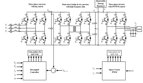
(STATCOMs) and unified power flow controllers (UPFCs), and so on [4]. Since renewable energy
47
resources (RESs) such as wind, fuel cells and solar have penetrated into the industry, so power
48
electronic converters also find their applications in them [5], [6]. Energy resources like natural coal or
49
gas are limited and use of RESs are growing constantly with the aim to exchange electric power with
50
the grid by net metering. Owing to the fact that the conventional transformer cannot be interfaced
51
with RESs and the progress made in the field of power electronics, have led to the evolution of
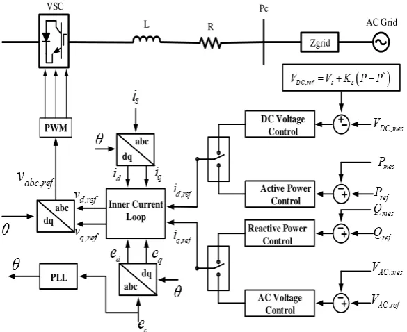
52
another power electronic converter named Solid State Transformer, also known as power electronic
53
transformer, that has grabbed a lot of attention [7]-[11].
54
With the progress made in the field of semiconductor industry, high-frequency controlled
55
switches with high-power ratings have been developed. With these advancements and to cope with
56
the future requirement of distributed energy sources integration, research is being carried out in the
57
field of power electronics which targets the use of SSTs in applications of high-power level. One of
58
the key interests of researchers is to develop a dynamic architecture of SST acquiring minimum
59
controlled switches; the other approach is integration of SSTs with RESs and other power applications
60
[19].
61
Solid State Transformers respond to control signals but their designs are not simple due to the
62
presence of power electronic converters. The basic principle of operation of SST is that it first
63
transforms low-frequency (50 Hz) AC voltage to high-frequency (frequency more than 20 kHz)
64
voltage. After that isolated dual active DC-DC high frequency converter regulates secondary dc
65
voltage, whose size is much smaller because of high frequency operation. The multi-stage power
66
electronic converters use controlled power electronic switches in series. In the first stage active
67
rectifier is used which converts and controls grid voltage to dc grid voltage and provides extended
68
control of active and reactive power [12]. Thus, it provides control of power and power factor. One
69
of the most important benefits provided by SST is that it isolates both primary and secondary side,
70
thus eliminating the coupling effects. Ride through capabilities, and compatibility between RESs and
71
grid make SST superior to conventional transformers [12]. The ability of SSTs to generate any variable
72
frequency voltage enables it to perform better and efficient in industry applications as it removes the
73
requirement of using variable frequency drives (VFDs). SSTs, in future, will not only replace the
74
conventional bulky transformers dominating at charge stations, locomotive and traction applications,
75
smart grids and at secondary distribution sides, but also provide additional functions, such as control
76
of active-reactive power and distribution source integration. Reduced-volume SST with
77
aforementioned features also plays a key role in improving the power quality [13], [14].
78
Various two-level and multilevel switching converter topologies can be employed in SSTs as
79
discussed in [15]. Some recent configurations of SST are also reported in [16]-[19]. SSTs in the form of
80
Direct AC to AC Matrix Converters directly convert three phase alternating current to three phase
81
alternating voltage [20]. SSTs without dc link are impossible to be interfaced with RESs and fuel cells
82
[21]. However, SST with a dc link [22] offers advantages such as availability of dc port, and much
83
reduced size due to high frequency operation over [20], [21]. But all aforementioned topologies
84
involve large number of converter valves. The isolated type topology, presented in this paper with
85
least possible controlled switches, completely isolates grid and load, and provides independent
86
control of voltage, frequency, power flow and power factor. The suggested topology of SST also can
87
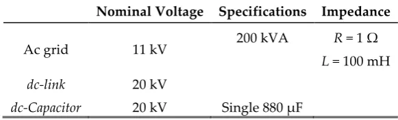
maintain clean voltage and current waveforms of utility supply irrespective of type and nature of the
88
load. This is what that has been stressed upon in this paper.
89
2. Proposed SST Circuit, Specifications and Control Layout
90
Vector control (decoupled controller) is used for three phase rectification purpose. Vector control
91
employing controlled switches such as IGBTs maintains THD of input current within IEEE defined
92
limits and provides ripple free dc output voltage. Obtained dc voltage VDC mes, is converted to high
93
frequency transformer. This stepped down voltage is rectified again with the help of full-bridge
95
converter as shown in Fig. 1. In the last stage, dc voltage Vx is converted back to variable three phase
96
G C E G C E G C E G C E G C E G C E G C E G C E G C E G C E G C E G C E G C E G C E G C E G C E G C E G C E G C E G C E LOAD o Three phase converterwith dq control
Dual active bridge dc-dc converter with high frequency link
Three phase inverter with SVPWM control
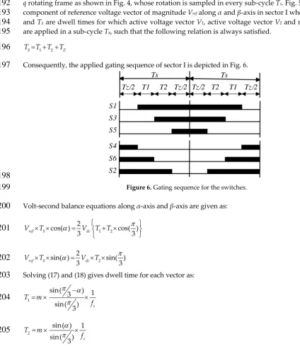
L R
C
C1
C2
+ _
L R
L R
Renewable Energy Resource
,mes
DC
V Vx
a V b V c V
Gate pulses for SST-VSC
Gate pulses for SST-VSI d V q V d i q i ,
DC ref
V Decoupled Controller Space Vector PWM out f out f x V out V out V + _
S1' S3' S5'
S4' S6' S2'
S1 S3 S5
S4 S6 S2
S7' S9'
S10'
S7 S9
S10 S8
S8'
97
Figure 1. Proposed circuit diagram of Solid State Transformer.
98
voltage with frequency and voltage control using Space Vector Pulse Width Modulation (SVPWM)
99
technique.
100
2.1. Control Layout Of SST-Voltage Source Convereter
101
Flux-oriented vector current control (VOC), based on two control layers: outer current control
102
layer (OCC) and inner current control layer (ICC), is used to control the operation of voltage source
103
converters (VSCs) [23]. The outer layer satisfies the dc voltage, active power and reactive power
104
demands of the VSCs while the inner layer uses decoupling control method to regulate the q-axis and
105
d-axis currents. Both control loops have a proportional and integral (PI) controller as common element
106
in them. DC link voltage VDC mes, is regulated using voltage droop control [24]. Through the
107
investigation of bi-layer control architecture deployed within multi-input multi-output (MIMO) voltage
108
source converter, it can be realized that the operation of SST-VSC becomes a bit complex [25]. This
109
complex control architecture has many variables which need to be controlled precisely using PI
110
controllers [26]. Therefore, it is requirement of the system that PI controllers should be optimally tuned
111
to provide both transient and steady state desired responses. But, tuning PI parameters of the nonlinear
112
system like voltage source converter, is a challenging task within itself [27].
113
Vector current control is used at point of common coupling, which regulates the dc voltage control
114
at VSC and power flow control with ac voltage regulation [28]. In this technique, ac voltage and current
115
of the VSC are converted into rotating d-q reference frame, which is synchronized with ac grid voltages
116
using phase locked loop (PLL). This methodology not only regulates dc and ac voltage but also provides
117
the decoupled control of both active and reactive power. The layout of d-q control architecture-based
118
SST-VSC is shown in Fig. 2. The outer control loop produces reference currents for inner current loop,
119
which then provides the reference voltage for the d-q reference frame.
120
By taking d-q control frame into consideration, internal control loop uses PI controllers which
121
generate reference current and maintain required voltage for the VSCs. Voltage expression at the point
122
of common coupling (pc) and voltage source converter side (vs) can be given as:
PWM
VSC
AC Grid
Zgrid Pc
R
Active Power Control DC Voltage
Control
AC Voltage Control Reactive Power
Control
PLL
Inner Current Loop abc
abc
abc dq dq
dq
L
124
Figure 2. The d-q control architecture of SST-VSC.
125
− = + S
C S S
di
e v R i L
dt (1)
126
where R and L represent resistance and inductance between SST-VSC and PCC, while iS is the current
127
from grid to the SST-VSC.
128
From Park’s transformation:
129
− = − + d
d d d q
di
e v Ri Li L
dt (2)
130
− = + + q
q q q d
di
e v Ri Li L
dt (3)
131
Here
represents the angular frequency at PCC of ac system. Based on (2) and (3), ICC control132
layout is shown in Fig. 3. The reference signals(Vd ref_ andVq ref_ )are transformed back to abc frame,
133
which are used to generate switching pulses for IGBTs of VSC.
134
id_ref
id
iq_ref iq
P, I
P, I
ωL
ωL
+
-
+
-
-
+
+
+
-
-
Vd_ref Vd
Vq_ref
Vq
135
In this research, classical tuning method is used to tune the PI controller parameters. The transfer
137
function of simple PI controller is:
138
= +
( ) i
p
k F s k
s
(4)
139
According to internal model control (IMC) method as presented in [29], we can write:
140
−
= + ) 1 = +
( ) ICC ( ) ICC( )
p
F s k G s R sL
s s
141
= +
( ) ICC ICC R
F s L
s
(5)
142
Here ICC (rad/s) represents the bandwidth of the current controlled system; G s)( ) is the
143
estimation of G s( ). Comparison of (4) and (5) yields the range of PI controller coefficients for ICC as:
144
,
p ICC ICC
k L (6)
145
,
i ICC ICC
k R (7)
146
The bandwidth ICC for the ICC must be selected such that it is ten times lesser than the
147
switching frequency [30], [31]. That is to say:
148
2
10
ICC
Fs
(8)
149
The PI controller parameters for the OCC can also be tuned using the same procedure as for ICC
150
but with a constraint that OCC must be ten times slower than the ICC to achieve the non-oscillatory
151
response of the closed loop system. This is achieved by selecting bandwidth of the OCC such that it
152
is 10 times smaller than the bandwidth of the ICC. As presented in [32], the OCC PI controller
153
parameters are given as:
154
,
p OCC OCC
k C (9)
155
2
,
i OCC OCC
k C (10)
156
10
ICC
OCC
(11)
157
Outer control loop is responsible for controlling ac and dc voltage, both active and reactive
158
powers at PCC. As shown in Fig. 2, d-channel controls dc link voltage or active power control, while
159
the q-channel regulates ac voltage or controls the reactive power. These relations are mathematically
160
represented as:
161
= d d+ q q
P V i V i
(12)
162
= q d− d q
Q V i V i
(13)
163
Using PLL, d-axis of vector control is synchronized with phasor voltage of the ac system. So,
164
=0
q
V . This reduces (12) and (13) to:
165
= d d
P V i (14)
166
=− d q
Q V i (15)
167
From (14) and (15), active power and reactive power is regulated by controlling d-q axis currents.
168
reactive power to the system. Likewise, dc link voltage is maintained via exchange of real power with
170
ac system or by modifying the d-axis current.
171
The specifications of the VSC used within SST are given in Table 1:
172
Table 1. VSC Specifications for SST.
173
Nominal Voltage Specifications Impedance
Ac grid 11 kV 200 kVA R = 1 Ω
L = 100 mH
dc-link 20 kV
dc-Capacitor 20 kV Single 880 μF
2.2. Control Layout Of SST-Voltage Source Inverter
174
Three phase two level voltage source inverters (VSIs), consisting of two power electronic
175
switches in each leg, have penetrated in the industry as they provide various speed control demands
176
of induction motor drives. Two level VSI has six active states and two null states. Various PWM
177
techniques are proposed in [33], [34] to reduce the VSI output waveform distortions at given
178
switching frequency. The most popular one is Space Vector PWM as it provides low output current
179
ripple and provides maximum utilization of the dc-link voltages [35], [36]. It provides 15% higher ac
180
voltage, lower current and voltage harmonics distortions as compared to conventional PWM [37].
181
This is the reason that SVPWM as modulation technique is employed in this research. The active
182
states divide the space vector plane into six sectors of equal magnitude as shown in Fig. 4. Switching
183
states for all eight (six active and two null) vectors are shown in Table 2.
184
Vref V3(010)
V6 (101)
V8 (000)
V2(110)
V4(011)
V7 (111)
α
d-axis V1(100)
V5 (001)
q-axis
V1 (100) V4 (011)
V2 (110) V3 (011)
185
Figure 4. Vector representation of SVM signal.
186
o β
α 600
α Vdc T1/Ts ×V1
Vdc
Vref
T2/Ts ×V2
187
Table 2. Space Vectors State and Switching Sequence.
189
Vector Sector & Vector Combination Line to Line Voltage State
Vab Vbc Vca
V0 (000) 0 0 0 Zero
V1 (100) I V0, V1, V2, V7 +Vd 0 -Vd Active
V2 (110) II V7, V2, V3, V0 0 +Vd -Vd Active
V3 (010) III V0, V3, V4, V7 -Vd +Vd 0 Active
V4 (011) IV V7, V4, V5, V0 -Vd 0 +Vd Active
V5 (001) V V0, V5, V6, V7 0 -Vd +Vd Active
V6 (101) VI V7, V6, V1, V0 +Vd -Vd 0 Active
V7 (111) 0 0 0 Zero
190
Using SVPWM, desired three phase voltages are provided by the voltage vector controlled in
d-191
q rotating frame as shown in Fig. 4, whose rotation is sampled in every sub-cycle Ts. Fig. 5 shows the
192
component of reference voltage vector of magnitude Vref along α and β-axis in sector I whereas, T1, T2
193
and Tz are dwell times for which active voltage vector V1, active voltage vector V2 and null vectors
194
are applied in a sub-cycle Ts, such that the following relation is always satisfied.
195
= + +1 2
S Z
T T T T (16)
196
Consequently, the applied gating sequence of sector I is depicted in Fig. 6.
197
Tz/2
T1
T2
Tz/2
Tz/2
T2
T1
Tz/2
Ts
Ts
S1
S3
S5
S4
S6
S2
198
Figure 6. Gating sequence for the switches.
199
Volt-second balance equations along α-axis and β-axis are given as:
200
= +
1 2
2
cos( ) cos( )
3 3
ref S dc
V T V T T (17)
201
sin( )=2 2 sin( )
3 3
ref S dc
V T V T (18)
202
Solving (17) and (18) gives dwell time for each vector as:
203
−
=
1
sin( ) 1
3 sin( )
3 s
T m
f (19)
204
=
2
sin( ) 1 sin( )
3 s
T m
f (20)
= −( 1+ 2)
Z S
T T T T (21)
206
where ‘m’ represents modulation index which is equal to Vref
(
2 3Vdc)
and fs=1Ts207
represents the switching frequency.
208
The specifications of the VSI used within SST are given in Table 3.
209
Table 3. VSI Specifications for SST.
210
Quantity Specifications
dc- link Input DC Voltage 500 V
dc- Capacitors 2-dc capacitors in series Each 250 V
& 20 mF
Vout Output Voltage Variable
Fout Output Frequency Variable
2.3. Ferrite Core High Frequency Transformer Design
211
The importance of ferrite materials is worth mentioning in modern power and industrial
212
electronics application. Design constraints of ferrite materials and losses incorporated in soft
213
magnetic materials due to high switching frequency are already discussed in literature [38], [39].
214
More elaborate models which discuss the modelling and dependence of ferrite losses at high flux
215
densities and high frequencies are also discussed in [40].
216
The operation of ferrites at square waves with 50% duty cycle offer 0-15% smaller losses as
217
compared to sinusoidal signals of same peak and frequency [41]-[44]. These properties and
218
performance make ferrite materials suitable for many switching applications where square wave
219
switching is desired without using any auxiliary filter circuits.
220
In this research work ferrite medium, operated at 50% duty cycle within DAB, is used not only
221
to provide galvanic isolation but also to decrease voltage levels. ANSYS/Maxwell platform is chosen
222
to design the high frequency ferrite core transformer. The specified design parameters of simulated
223
Maxwell model, as shown in Fig. 7, are tabulated in Table 4.
224
(a) (b)
Figure 7. High frequency ferrite core transformer. (a) Primary and secondary coil. (b) Complete
225
transformer model placed within air medium.
226
The parameters of high frequency transformer, simulated using ANSYS/Maxwell software,
227
Table 4. Parameters of High Frequency Ferrite Transformer.
229
Units Quantity Values
3F3 Ferrite (MnZn), P-Type 9997 (nH/T2)
B Magnetic flux density 3200 Gauss (core losses < 100
mW/cm3)
WaAc Product of Core Area and Window Winding Area 1006.7857 cm4
Ac Core Area 25cm2
Wa Window Winding Area 40.271429 cm2
Po Power 200 kVA
F Frequency 25 kHz
J Current Density 3.5 A/mm2
K Filling Factor 0.6
Vp Primary Voltage 20 kV
Ip
Primary Current (with 5% increase in input power to
cover losses) 10.5 A
Vs Secondary Voltage 500 V
Is Secondary Current 400 A
Np Primary Turns 250 Turns
Ns Secondary Turns 7 Turns
Rp Primary Winding Resistance 0.299947 Ω
Lp Primary Winding Inductance 26676.98 μH
Rs Secondary Winding Resistance 0.34242 mΩ
Ls Secondary Winding Inductance 400.904 μH
Apw
Primary Winding Wire Area (with skin effect
compensation) 4.399 mm
2
Asw
Secondary Winding Wire Area (with skin effect
compensation) 122.23 mm
2
230
3. Simulation Results
231
The SST-VSC incorporated within inner-outer control loops and voltage droop control maintains
232
both active and reactive power requirements while the SST-VSI fulfills variable frequency control
233
requirements at the consumer end. The SST-VSC connected with 11 kV grid, maintains dc-link
234
,
DC mes
V at 20 kV whose specifications are already given in Table I, while the SST-VSI, specifications
235
given in Table 2, generates variable voltage and variable frequency at the load end.
236
Since the proposed circuit is symmetric, so the bidirectional power flow can be achieved just by
237
changing the gate pulses only without any amendment in the circuit. To assess the flexibility and
238
validity of the proposed circuit, simulations using MATLAB/Simulink environment are carried out
239
for four different test cases: SST to deliver active power, SST as a variable frequency drive,
240
bidirectional power flow interfacing RES, and SST as a power factor improvement (PFI) device.
241
3.1. Case 1: Active Power Flow
242
Simulation results are presented at various stages of the proposed SST based on multi-stage
243
power switching converters after the transient period is elapsed. Three phase voltage and current at
244
(phase A) at grid side remain in-phase even active power demand is varied from 0.0 p.u. to 1.0 p.u,
246
thus delivering power at unity power factor. Results show that presented SST model draws balanced
247
three phase current from the grid. Input current (phase A) has very less harmonic content (THD =
248
2.16%) as shown in Fig. 10. Same results are valid for other phases as well.
249
250
(a) (b)
Figure 8. (a) SST input voltage at grid side. (b) SST input current at grid side.
251
252
Figure 9. Result displaying that phase A voltage and current are in phase with each other.
253
(a) (b)
Figure 10. (a) Phase A current drawn from utility (b) THD analysis of phase A current.
254
256
FIGURE 11. SST-VSC voltage and current at dc-link
257
In dual active bridge (DAB) circuit, the full bridge square wave inverter cascaded at SST-VSC
258
generates square wave voltage of 25 kHz for the high frequency transformer (HFT), which reduces
259
voltage level. The other full bridge square wave converter used within DAB, rectifies the voltage at
260
secondary side of HFT. The voltage and current response of the SST-VSC at dc-link VDC mes, side is
261
given in Fig. 11. Voltage at primary and secondary side of HFT are shown in Fig. 12.
262
263
FIGURE 12. Primary and secondary voltage of high frequency transformer.
264
At the DAB end, dc-capacitor decreases the ripple content while the SST-VSI cascaded uses
265
SVPWM pulses to generate three phase voltage with variable frequency and amplitude for the
266
consumer end. When generated frequency is 50 Hz, the SST-VSI output L-N voltage before and after
267
(a) (b)
Figure 10. (a) SST-VSI output voltage without filter. (b) Filtered SST output Voltage.
269
3.2. Case 2: SST as Variable Frequency Drive
270
When the operation of SST as VFD is evaluated for the case when SST delivers power to an
271
induction motor with 1.0 p.u mechanical loading, the obtained results show satisfactory results. SST
272
maintains unity power factor. The grid side current harmonic contents are within IEEE defined THD
273
limits. With induction motor at rated loading, settling time of SST-VSC at dc-link increases by 0.15 s,
274
as shown in Fig. 14. SST-VSC takes a little bit more (0.32 s) time to settle for the inductive load.
275
For the case when SST generates voltage signal of 50 Hz for the inductive load, it can be observed
276
from Fig. 15 that SST input current and the voltage are in phase, thus ensuring unity power factor.
277
For this case, filtered SST output voltage is show in Fig.16.
278
When SST generates 60 Hz voltage signal for the load, same parameters are evaluated, as in for
279
previous case, and are displayed in Fig. 17. Similarly, a voltage signal of other frequencies can be
280
generated using the proposed SST for the resistive as well as the inductive load.
281
282
284
FIGURE 15. Result displaying that phase A voltage and current are in phase.
285
286
FIGURE 16. SST 50 Hz filtered output voltage.
287
(a) (b)
FIGURE 17. SST simulation results for 60 Hz output. (a) Phase A voltage and current in phase. (b)
288
3.3. Case 3: SST with a Renewable Interface
290
To cope with the increasing trend of using RESs, SST provides a very handy infrastructure. RES
291
integrated with SST, as shown in Fig. 1, can be used solely to provide power to consumer, making
292
SST working as stand-alone system. The proposed topology also makes bidirectional power flow
293
possible just by changing the gate pulses of the SST-VSC to make it perform as SST-VSI.
294
High frequency transformer, which in previous cases was used to reduce the voltage level, now
295
in this scenario, is working as step up HFT. DAB, in this case, will maintain dc-link for the SST-VSC.
296
The SST-VSC, now working as SST-VSI, uses SVPWM pulses to generate three phase voltage. In this
297
scenario SST is working as grid-tied inverter, feeding power to the utility.
298
The RES block, represented in Fig. 1, would be any single RES or the hybrid-RES incorporating
299
batteries as well. In this research work, only the design of controlled multi-input multi-output
300
circuitry of SST is under investigation. So, no specific constraints regarding the RESs are taken into
301
consideration.
302
When a constant dc source is used as RES, simulations show that SST provides power not only
303
to consumer but also to the utility as well, as shown in Fig. 18.
304
So, this architecture provided by SST would be a solution to all problems, that will be faced in
305
the future when smart and super grids will be kicked in the power system.
306
307
(a) (b)
FIGURE 18. SST simulation results when integrated with renewable energy resource (a) SST line to
308
neutral voltayge at consumer end. (b) SST line to line voltage at grid end.
309
3.4. Case 4: SST as a Power Factor Improvement Device
310
In the ICC of SST-VSC, quadrature component of current is maintained at zero using PI
311
regulation, which forces SST not to draw reactive power from the grid, thus maintaining unity power
312
factor at the grid side. When the q-component of current in ICC is maintained at any positive value,
313
SST draws leading VAR from the grid, making SST as a PFI device, and at the same time maintaining
314
its own feature of transformer.
315
When the current at grid side was set to 45o leading, simulation result shows that SST maintains
316
its function of PFI device when it is delivering power to a 1 p.u. rated inductive load. As compared
317
to the conventional transformers, this is remarkable achievement of the proposed SST design.
318
Proposed circuit as a part of interconnected system has the ability to improve the overall power factor
319
of the system while meeting the lagging reactive power requirement of the load. However, the
320
current at the grid side increases as expected. Fig. 19 shows voltage and current of phase A at grid
321
side, and filtered output voltage of the SST.
322
When SST as a PFI device is investigated by the pre-tuned PI controller parameters, simulation
323
droop control at the outer layer of the VSC can be re-tuned to reduce the settling time of the
SST-325
VSC.
326
(a) (b)
FIGURE 19. SST simulation results as PFI device (a) Input current leads input voltage. (b) SST filtered
327
output voltage.
328
329
FIGURE 20. SST-VSC response working as PFI device with induction motor loading.
330
4. Conclusions
331
To replace conventional bulky transformers, reduced-size ‘isolated’ SST is proposed in this
332
research. Either the source is single phase or three phase or dc source, proposed SST model can
333
generate single phase or three phase or dc voltage for any type of resistive or inductive load. When
334
interfaced with RES, symmetric configuration of SST makes it working as a stand-alone system at
335
consumer end as well as grid-tied inverter at grid side. Simulation results are assessed for scenarios
336
where SST acts as a variable frequency drive and as a power factor improvement device. In addition,
337
when interfaced with RES, SST ensures bidirectional power flow as well. Simulation results validate
338
the performance of the proposed SST for all the scenarios. Working of SST as VFD and PFI device
339
with renewable interface makes it ideal for industrial applications where the proposed SST topology
340
may eliminate the requirements of bulky conventional transformer especially for motor drive
341
applications. This justifies the role of SST as VFD. The four quadrant operation of controlled switches
342
with dc port within SST enables it to be integrated with micro/super grids. Proposed SST design has
343
consumer end. The presented topology of SST can easily support the wide range operation of
345
distribution system. The future work would be development of hardware setup for the proposed SST
346
topology, thus to check the validity of the proposed SST model on real time industrial applications.
347
Apart from SST design, optimized integration of SST with hybrid-RES would be a design worth of
348
importance.
349
Author Contributions: U.T, D.O.G, G.A., U.F., A.R. and M.U.A. suggested the idea, performed the simulations
350
and managed the paper. V.E.B., M.B and J.G. assisted in the idea development and paper writing.
351
Funding: This research received no external funding.
352
Conflicts of Interest: The authors declare no conflict of interest.
353
References
354
355
1. J. S. Lai, A. Maitra, A. Mansoor, and F. Goodman, “Multilevel intelligent universal transformer for medium
356
voltage applications,” in Proc. IEEE Industry Applications Conference, 2-6 Oct. 2005, pp. 1893-1899.
357
2. E. R. Ronan, S. D. Sudhoff, S. F. Glover, and D. L. Galloway, “A power electronic-based distribution
358
transformer,” IEEE Trans. Power Del., vol. 17, no. 2, pp. 537-543, 2002.
359
3. U. Tahir, S. A. Ali, O. Azeem, O. Khan and R. Muzzammel, “THD improvement of phase voltages via
360
injection of voltage in neutral conductor for three phase four wire distribution system,”2018 International
361
Conference on Computing, Mathematics and Engineering Technologies (iCoMET), Sukkur, 2018, pp. 1-5.
362
4. N.G. Hingorani, Understanding FACTs: concept and technology of flexible AC transmission systems. New York:
363
IEEE press, 2000.
364
5. Z. Chen, J. M. Guerrero, and F. Blaabjerg, “A review of state of art power electronics for wind turbines,”
365
IEEE Trans. Power Electron., vol.23, no.8, pp.1859-1875, Aug.2009.
366
6. J. M .Carrasco, L. G. Franquelo, J. T. Bialasiewicz, E. Galvan, R. C. P .Guisado, M. A. M. Prats, J. I. Leon,
367
and N. Moreno-Alfonso, “Power Electronic Systems for the Grid integration of Renewable Energy Sources:
368
A survey,” IEEE Trans.Ind.Electron., vol.53, no.4, pp.1002-1016, June 2006.
369
7. S. Bifaretti, P. Zanchetta, A. Watson, L. Tarisciotti, and J. C. Clare, “Advanced power electronic conversion
370
and control system for Universal and Flexible Power Management,” IEEE Trans.smart grid., vol.2, no.2,
371
pp.231-243, June 2011.
372
8. T. F. Zhao, L. Y. Yang, J. Wang, and A. Q. Huang, “270kVA Solid State Transformer Based on 10kV SiC
373
Power Devices,” in Proc.IEEE.Electric Ship Tech. Symp., 2007, pp.145-149.
374
9. G. Y. Wang, S. Baek, J. Elliott, A. Kadavelugu, F. Wang, X. She, S. Dutta, Y. Liu, T. F. Zhao, W. X. Yao, R.
375
Gould, S. Bhattacharya, and A. Q. Huang, “Design and hardware implementation of Gen-I silicon based
376
solid state transformer,” in Proc.IEEE.Appl.Power Electron.Conf., 2011, pp.1344-1349.
377
10. X. She, A. Q. Huang, and G. Y. Wang, “3-D space modulation with voltage-balancing capability for a
378
cascaded seven-level converter in a solid state transformer,” IEEE Trans.Power Electron., vol.26, no.12,
379
pp.3778-3789, Dec.2011.
380
11. D. Grider, M. Das, A. Agarwal, J. Palmour, S. Leslie, J. Ostop, R. Raju, M. Schutten, and A. Hefner,
381
“10kV/120A SiC DMOSFET Half-bridge Power Modules for 1MVA Solid State Power substation,” in
382
Proc.IEEE.Electric Ship Tech. Symp., 2011, pp.131-134.
383
12. A. Al-Hafri, H. Ali, A. Ghias and Q. Nasir, “Transformer-less based solid state transformer for intelligent
384
power management,”2016 5th International Conference on Electronic Devices, Systems and Applications
385
(ICEDSA), Ras Al Khaimah, 2016, pp. 1-4.
386
13. P. Drabek, Z. Peroutka, M. Pittermann, and M. Cedl, “New configuration of traction converter with
387
medium-frequency transformer using matrix converters”, IEEE Trans. Ind. Electron., vol. 58, no. 11, pp.
388
5041-5048, Nov. 2011.
389
14. X. She, A. Q. Huang, F. Wang, and R. Burgos, “Wind energy system with integrated active power transfer,
390
reactive power compensation, and voltage conversion functions”, IEEE Trans. Ind. Electron, vol. 60, no. 10,
391
pp. 4512-4524, Oct. 2013.
392
15. S. Falcones, X. Mao, and R. Ayyanar, “Topology comparison for solid state transformer implementation,”
393
16. K. Basu and N. Mohan, “A single-stage power electronic transformer for a three-phase PWM AC/AC drive
395
with source-based commutation of leakage energy and common-mode voltage suppression,” IEEE Trans.
396
Ind. Electron., vol. 61, no. 11, pp. 5881-5893, Nov. 2014.
397
17. S. Madhusoodhanan, A. Tripathi, D. Patel, K. Mainali, A. Kadavelugu, S. Hazra, S. Bhattacharya, and K.
398
Hatua, “Solid state transformer and MV Grid tie applications enabled by 15 kV SiC IGBTs and 10 kV SiC
399
MOSFETs based multilevel converters,” IEEE Trans. Ind. Appl., vol. 51, no. 4, pp. 3343-3360, Jul.-Aug. 2015.
400
18. L. Wang, D. Zhang, Y. Wang, B. Wu, and H. S. Athab, “Power and voltage balance control of a novel three
-401
phase solid-state transformer using multilevel cascaded H-bridge inverters for microgrid applications,”
402
IEEE Trans. Power Electron., vol. 31, no. 4, pp. 3289-3301, Apr. 2016.
403
19. Xu She, Alex Q. Huang and Rolando Burgos, “Review of Solid-State Transformer Technologies and Their
404
Application in Power Distribution Systems,” IEEE Journal of Emerging and Selected Topics in Power Electronics,
405
Vol. 1, No. 3, pp.-186-198, Sept. 2013.
406
20. R. Muzzammel and U.Tahir, “Maximization of Transfer Ratio and Minimization of Harmonics in Three
407
Phase AC/AC Matrix Converter,” British Journal of Applied Science & Technology, ISSN: 2231-0843,Vol.: 21,
408
Issue. 2, 2017
409
21. H. Chen and D. Divan, "Design of a 10-kV·A Soft-Switching Solid-State Transformer (S4T)," in IEEE
410
Transactions on Power Electronics, vol. 33, no. 7, pp. 5724-5738, July 2018.
411
22. Reddy, B. Dheeraj, Dr. Sahoo, Sarat Kumar,“Design of Solid State Transformer,” International Journal of
412
Advanced Research in Electrical, Electronics and Instrumentation Engineering, Vol. 4, Issue 1, January 2015.
413
23. G. Wu et al., “Analysis and design of vector control for VSC-HVDC connected to weak grids,” CSEE J.
414
Power Energy Syst., vol. 3, no. 2, pp. 115-124, Jun. 2017.
415
24. K. Rouzbehi, A. Miranian, J. I. Candela, A. Luna, and P. Rodriguez, “A generalized voltage droop strategy
416
for control of multiterminal DC grids,” IEEE Trans. Ind. Appl., vol. 51, no. 1, pp. 607-618, Jan./Feb. 2015.
417
25. K. Rouzbehi, W. Zhang, J. I. Candela, A. Luna, and P. Rodriguez, “Unified reference controller for flexible
418
primary control and inertia sharing in multi-terminal voltage source converter-HVDC grids,” IET Gener.,
419
Transmiss. Distrib., vol. 11, no. 3, pp. 750-758, Feb. 2017.
420
26. A. Raza, X. Dianguo, L. Yuchao, S. Xunwen, B. W. Williams, and C. Cecati, “Coordinated operation and
421
control of VSC based multiterminal high voltage DC transmission systems,” IEEE Trans. Sustain. Energy,
422
vol. 7, no. 1, pp. 364-373, Jan. 2016.
423
27. Z.-L. Gaing, “A particle swarm optimization approach for optimum design of PID controller in AVR
424
system,” IEEE Trans. Energy Convers., vol. 19, no. 2, pp. 384-391, Jun. 2004.
425
28. L. Xu, “Modeling, analysis and control of voltage-source converter in microgrids and HVDC,” M.S. thesis,
426
Univ. South Florida, Tampa, FL, USA, Nov. 2013.
427
29. OTTERSTEN ROLF. “On Control of Back‐to‐Back converters and Sensorless Induction Machine Drives”. PhD
428
Thesis, Department of Electric Power Engineering, Chalmers University of Technology, Göteborg, Sweden.
429
2003. 165p. ISBN: 91‐7291‐296‐0.
430
30. K. Rouzbehi, A. Miranian, A. Luna, and P. Rodriguez, “Optimized control of multi-terminal DC grids using
431
particle swarm optimization,” Eur.J. Power Electron., vol. 24, no. 2, pp. 38-49, 2014.
432
31. R. T. Pinto, P. Bauer, S. F. Rodrigues, E. J. Wiggelinkhuizen, J. Pierik, and B. Ferreira, “A novel distributed
433
direct-voltage control strategy for grid integration of offshore wind energy systems through MTDC
434
network,” IEEE Trans. Ind. Electron., vol. 60, no. 6, pp. 2429-2441, Jun. 2013.
435
32. S. Rodrigues, “A multi-objective optimization framework for the design of offshore wind farms,” Ph.D.
436
dissertation, Delft Univ. Technol., Delft, The Netherlands, 2016.
437
33. J. Holtz, “Pulse width modulation for electronic power conversion”, Proc. IEEE, vol. 82, no. 8, pp.
1194-438
1214, Aug, 1994.
439
34. D. G. Holmes and T. A. Lipo, Pulse Width Modulation for Power Converters: Principles and Practice.
440
Hoboken, NJ:Wiley, 2003.
441
35. J. Rodriguez, J. S. Lai and F. Z. Peng, “Multilevel Inverters: A survey of topologies, controls, and
442
applications”, IEEE Trans. Ind.Electr., vol. 49, no. 4, pp. 724-738, Aug. 2002.
443
36. A. C. Binojkumar, J. S. Siva Prasad, and G. Narayanan, “Experimental investigation on the effect of
444
advanced bus-clamping pulse width modulation on motor acoustic noise,” IEEE Trans. Ind.Electr, vol. 60,
445
no. 2, pp. 433-439, Feb. 2013.
446
37. A. Kumar and D. Chatterjee, “A survey on space vector pulse width modulation technique for a two-level
447
38. G. Bertotti, ‘Hysteresis in magnetism’, Academic Press, San Diego, USA, 1998, pp. 225-429.
449
39. R. Boll, ‘Soft Magnetic Materials’, The Vacuumschmelze Handbook, Heyden&Son Ltd., London, UK, 1979,
450
pp. 13-108.
451
40. C.R. Sullivan, “Winding loss calculation with multiple windings, arbitrary waveforms and 2-D field
452
geometry,” IEEE IAS Annual Meeting,1999, pp. 2093-2099.
453
41. J. Li, T. Abdallah and C. Sullivan, “Improved calculation of core loss with non-sinusoidal waveforms,”
454
IEEE, IAS 36-th Annual Meeting, Chicago, USA, September 30 – October 4, 2001, pp. 2203-2210.
455
42. E. C. Snelling, “Soft Ferrites Properties and Applications”, 2ndedition, London, UK., Butterworth, 1988.
456
43. A. V. Bossche, V. C. Valchev, G. B. Georgiev, “Measurement and Loss Model of Ferrites with Non
-457
sinusoidal Waveforms”, PECS’04, Aachen, Germany, 24-28 June, 2004.
458
44. V. C. Valchev, A. P. Van den Bossche and D. M. Van de Sype, "Ferrite losses of cores with square wave
459
voltage and DC bias," 31st Annual Conference of IEEE Industrial Electronics Society, 2005. IECON 2005.,