A Real – Time Research Platform for Extraocular
Image Processing of Epiretinal Prosthesis
Sharmili N#, Seetha Ramaiah P+
#,+
CS&SE Department, Andhra University Visakhapatnam, AP, India
Abstract— Epiretinal prosthesis has restored vision in blind patients who lost vision as a consequence of retinal degeneration. Epiretinal Prosthesis (EP) system is composed of three units, extraocular image processor, intraocular stimulator and wireless telemetry. The main challenge in EP system design is not to get a signal through to the brain, but to improve the resolution and detail of that signal. To improve the details of the signal, a research platform is needed for verifying and validating the vision/image processing software. This paper presents a real time research platform dedicated to the development of Extraocular Image Processing System (EIPS) for EP which includes a camera, an image processor, an encoder and a transmitter. In EIPS, images captured by camera are processed to match the resolution of electrode array and encoded into 1Mbps bit stream by microcontroller based image processing unit. The bit stream is modulated and transmitted to the internal stimulator through wireless telemetry. The research platform allows development and evaluation of various image processing algorithms to improve the quality of visual stimulation for EP with greater ease and flexibility. The system functionality is verified using the video display on LCD/LED array and is adaptable for product development for EP.
Index Terms— Epiretinal prosthesis, Image acquisition,
Image Processing, Image encoding, Amplitude shift keying (ASK), dual-band telemetry.
I. INTRODUCTION
OUR EYES are one of the five specialized sensory organs with which our mind uses to form a picture of world. The input to the visual system is light rays. The vision processing begins when the lens focuses light entering the eye on to the retina. Retina is a complex network of light sensitive neural cells namely photoreceptors, horizontal cells, bipolar cells, amacrine cells and ganglion cells. The photoreceptor cells capture light energy and convert it into electrochemical signals. The bipolar cells and amacrine cells mainly do image processing such as motion and contrast and transmit the signals to 1.2 million ganglion cells whose axons collectively form the optic nerve. The optic nerve transmits the visual information to the visual cortex at the back portion of the brain where the electrical signals are interpreted by the brain as a visual image. Blindness can result when any step of the optical pathway sustains damage.
Epiretinal Prosthesis (EP) is a device that can provide sight to people who are visually impaired as a consequence of degenerative retinal diseases such as Retinitis
Pigmentosa and Age-Related Macular Degeneration. Epiretinal prosthesis namely Argus II (http://www.2-sight.eu) has recently emerged as first commercially available visual prosthesis which encourages other research groups to develop their own versions of visual prostheses. This prosthesis maps real time video from environment to electrical pulses and stimulates the surviving healthy parts in the retina i.e. ganglion cells using electric pulses applied through an electrode array. Most of the researchers use biphasic pulses for stimulation of nerves so that no net charge should be transferred from the electrode into tissue. Many research groups attempted to design as well as implement epiretinal prostheses in terms of external devices and internal implants to achieve the same goal of vision restoration [1]-[10] [12]. Research groups Second sight, Australian Vision group and Nano Retina Projects are still continuing their research in RP, but not all of these devices have yet reached the clinical trial stage. Currently, only the Second Sight’s Argus II prosthesis has received the CE (Conformite Europeene) mark and FDA (U.S. Food and Drug Administration) approval [1] for use in the United States and the European Economic Area.
The state-of-the-art implantable retinal prosthesis does not provide sufficient vision to patients due to its limited number of pixels, which leads to a demand for higher resolution retinal prostheses. Many researchers say that minimum number of 600-1000 electrodes will be needed for the blind to recognize objects or walk around without assistance. Here the important one is the vision-processing software that picks up the image and transforms it into electrical impulses. Research in this area is focused on signal-processing circuitry with limited electrode resolution for better visual perception. This requires the development of a vision processing research platform for designing, implementing and testing new experiments in vision/image processing for epiretinal prosthesis. This platform should be flexible to design intricate experiments without requiring advanced programming skills or major hardware investment.
This paper presents a real time research platform for Extraocular Image Processing System (EIPS) for Epiretinal Prosthesis (EP) capable of full EIPS verification, individual functional block characterization and fast emulation. The standalone, portable microcontroller based research platform is able to perform real time image acquisition, image processing and image encoding and RF based wireless transmission for artificial vision.
Fig.1. The block diagram of the research platform for epiretinal prosthesis
To meet the real time requirements of vision processing for natural vision, the quality of stimulation depends on Pixel (i.e. electrode) brightness level, No of pixels (Resolution), Color depth (No of bits used to represent color), Refresh rate, Update rate. Normally 20 - 30 frames per second are required to view a good motion picture. To achieve flicker-free vision, the refresh rate is chosen to be 50 - 60 fps [49]. 32x32 size resolution i.e. 1024 electrodes are needed for doing common tasks such as walking without assistance, recognizing persons by seeing their faces and reading large text [7].
As the implants already on the market offer up to 60 electrodes (stimulation channels) in black and white, our aim is to develop a prototype extraocular image processing research platform to drive 1024 electrodes in size and 6 bit in color depth (grey scaled image representation) for better visual perception. In order to provide the real time video without flickering, the system can process images at 30 frames per second and the output verification is done using a 256 and channel LED arrays. The 256 and 1024-channel light-emitting diode (LED) array provides a one-to-one mapping with the transmitted image on LCD, that in turn drives to detect the malfunctioning any stimulation channel. This platform has an adequate capability to implement better algorithms than the standard image processing algorithms for better image prediction. The experimental results demonstrate that the proposed prototype model meets the design specifications of the epiretinal prosthesis system [1].
This paper is organized as follows. Section II presents the system architecture of the platform. Section III describes the detailed system-level circuit implementation. Section IV discusses the testing and validation of complete system. Finally, Section V is the conclusion.
II. ARCHITECTURE OF EPIRETINAL PROSTHESIS The hardware functional logic block diagram of the research platform for EPS is shown in figure 1. The system is composed of four major units: external part that can be worn on the body, internal part that is surgically placed under the retina, wireless telemetry which links external and internal parts. External part consists of a video camera, EIPS and a dual band power/data transmitter. EIPS captures the images using the camera, processes it in the data frame format to match the channel number and color depth of the stimulation array, then encodes and transmits the processed data frames serially to Amplitude Shift Keying (ASK) modulator for wireless transmission.
Both power and modulated data are transmitted from EIPS to the internal implant electronics through RF based dual band power/data transmitter. The internal portion consists of a power recovery circuit with its coil for power reception, ASK demodulator with its data coil for data reception, the RIRS for processing image data and stimulating the simulated LED electrode array which interfaces stimulator to the targeted tissue cells. For the data transmission, the ASK demodulator of intraocular retina stimulator receives the high-speed serial data at 1 Mbps rate from the secondary Platinum-Iiridium (Pt-Ir) Litz coil, demodulates and converts the received ASK modulated data into a bit stream, which is then decoded back to stimulation parameters. These parameters are distributed to all stimulation channels through stimulator for the generation of electrical pulses.
Sharmili N et al, / (IJCSIT) International Journal of Computer Science and Information Technologies, Vol. 6 (2) , 2015, 1134-1140
Fig.2. The implemented real time research platform for Extraocular image processing of epiretinal prosthesis.
Figure 2 shows the implemented research platform for epiretinal prosthesis which describes the hardware design details and measurement results. The research platform allows testing and evaluation of EIPS in the epiretinal prosthesis system and verifies the output of the system using a 256 and
1024-channel LED array and Liquid Crystal Display (LCD) for continuous images input at real time. The implementation of various image processing algorithms, working of RF based serial transmission, testing the encoded data at individual electrodes using the LED array can be emulated by JTAG based hardware debugger ("emulator") of the PIC32MX device. The PC provides an interactive user interface to investigate and control the embedded system circuits using MPLAB IDE software. The software architecture of this research platform is pliable and scalable to accommodate new features and research ideas for EPS. These strategic features leverage the platform to emerge as a successful tool in the research arena with many researchers utilizing it to implement new and existing algorithms in image processing for improving the visual perception.
III. SYSTEM LEVEL IMPLEMENTATION
In this section, the detailed circuit implementation of the Extraocular image processing system is designed using the functional modules such as CMOS camera, processor based body worn image processor and a RF based dual band power/data transmitter. The signal flow in extraocular image processing is shown in Figure 3. The Body Worn Image Processor (BWIP) is described in three parts: Image Acquisition, Image processing and Image encoding.
The laboratory model of extra ocular image processing system module is implemented on PIC32 microcontroller based SSD1928 Evaluation Kit (SSD1928 EK). All these tasks are developed with emulation software of PIC32 based SSD1928 EK and debugging is done on a laptop computer. The major advantage of using a PIC32 based SSD1928 EK and computer provides the flexibility of
evaluating various algorithms in real time and can be powered (3.7V 2700mAH Li-Ion) through battery. OV9650 CMOS Camera sensor fulfills the requirements of video sensor due to its logarithm characteristics and its on-chip ADCs and amplifiers.
Fig.3. Structure chart for BWIP.
A. Image Acquisition
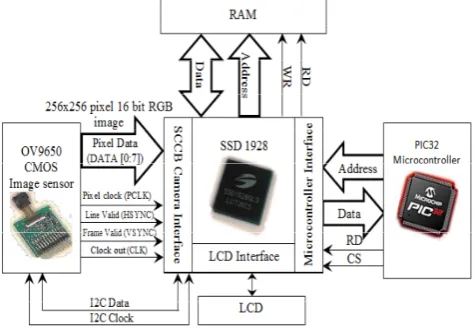
In the epiretinal approach, an embedded camera mounted in the frame of spectacles captures images and passes them to BWIP worn on the patient’s belt via a cable. The experimental setup for image acquisition using OV960 camera, PIC32 microcontroller and SSD 1928 Graphics controller is shown in figure 4.
Fig.4. Block diagram forinterfacing PIC32 with SSD1928
camera and LCD.
PIC32 based SSD1928 Evaluation kit was chosen due to its processor speed, low cost, open-source framework and the presence of a dedicated CMOS camera port on the chip that allowed the acquisition of images from the camera at a much higher frame rate than that of typical USB interfaces. SD1928 EVK provides a connector to interface camera with the processor. The connector exposes various data and control signals (managed by the OV9650 camera interface subsystem i.e Serial Camera Control Bus (SCCB)) as well as a single I2C channel [11][14]. SSD1928 uses the 10 bit Serial Camera Control Bus (SCCB) data interface to configure the features of the output image of the Omni Vision CAMERA CHIP by writing values into control registers. By configuring SCCB, the camera In System Programming (ISP) performs the additional operations, including data format conversion, brightness or contrast or saturation adjustment and image rescaling. It can transmit data in raw RGB (i.e., Bayer), RGB 565, RGB 555, YUV, or JPEG-encoded formats. Data can be transferred in parallel with separate synchronization signals (VSYNC, HSYNC, and HREF). Microcontroller based Image acquisition module acquires visual image from OV9650 CMOS camera sensor module by DMA through the fast parallel port known as Parallel Master Port.
Fig.5. Progressive scan of OV9650 Camera sensor.
Image data generation is done by progressive scanning of the array in which rows are sequentially read and transferred out to the Analog Processing Board inbuilt in camera. Through SCCB interface, data (DATA [7:0]) are read or scanned in synchronization with these VSYNC, HSYNC, HREF and PCLK control signals according to the polarity of enable signal (DV_ENB) to prevent flicker on display while updating the capturing data. Row and column drivers are inbuilt in camera for reading each pixel of an image. A row is selected by the row driver, then the column driver sequences through each of the columns. After each of the columns has been read, the row driver selects the next row and the process repeats till the total image is completed. The HREF signal is only valid when there is active output data. Image acquisition module uses the rising edge of PCLK to capture data when HREF is high. The vertical sync (VSYNC) signal resets both row and column drivers to the upper left pixel. The horizontal sync (HSYNC) causes the row driver to step to the new row. The VSYNC and HSYNC signals are continuous.
The SSD1928 camera interface receives the image data from the sensor and either writes it directly to memory or passes it on to one of the other modules (previewer or external memory like SD card) for further processing. The
received data may be formatted as raw RGB, YUV 4:2:2, or JPEG. YUV 4:2:2 Format is used for storing the images in SD Card in JPEG Format and RGB565 format for display the image on LCD.
The inbuilt resizer module of OV9650 camera module can able to up- or down-sample an image by a factor of four or less. We used downscaling for resizing the image for required resolution of electrode array 32x32. Resizer also preferred RGB 565 format. The main processor PIC32 microcontroller is used to configure SSD1928 for the operations / tasks mentioned above.
Fig.6. Image acquisition stored in SD card and output recorded onLCD.
The OV9650 Camera is tested by displaying the captured image information on LCD for real time video (continuous images) input. The captured input using OV9650 Camera and displaying output on LCD is shown in Figure 5. The resulting 32x32 pixel 16-bit RGB images (RGB565) are given to image processing module to explore prominent features of the image for better image recognition.
B. Image Processing
For blind people, it is difficult to predict exactly what they can perceive with such camera-driven visual prosthesis, which currently consists of tens of stimulating retinal electrodes, thereby allowing only for limited visual perception. Once acquiring an image stream from camera, image processing filters are applied before they enter into the visual prosthesis for better perception.
The only resources available for such an effort are confined to FPGA systems [5, 6] or costly DSP processors but in this research we will discuss the advanced pic32 microcontroller based development board of a low cost hardware based platform to perform image processing. One common factor that lies with most of the signal and image processing algorithms are highly computationally memory intensive. Embedded hardware always faces memory limitations. Although microchip PIC32 [7] is fully capable of implementing most signal processing tasks, it falls short of on-chip memory resources for image processing applications. If the system needs to incorporate a camera and an LCD to capture data and display it, the microcontroller needs to be interfaced with a special coprocessor SSD1928 [8] to overcome this memory limitation. Figure 3 shows a diagram interfacing PIC32 with SSD1928 camera and LCD. The main image Sharmili N et al, / (IJCSIT) International Journal of Computer Science and Information Technologies, Vol. 6 (2) , 2015, 1134-1140
processor that we are using in the project is Microchip’s 32-bit PIC32 microcontroller. This co-processor SSD1928 takes the load off the main processor so that it can fully utilize its resources on image processing algorithm implementation [13, 14].
In this the image information i.e. 32x32 image is taken from image buffer of co-processor SSD1928 and given to image processing module embedded in PIC32 microcontroller. After studying various image processing algorithms such as saliency based image processing and various edge detection algorithms in matlab, Canny Edge Detection is preferred for low resolution images. To implement an algorithm such as canny edge detection in hardware, it would first be implemented in Matlab without using built in functions. This will then be easily transferred to C implementation that can be converted to machine code.
Canny edge detection comprises of following steps: 1. Smoothing: Blurring of the image to remove noise.
2. Finding gradients: The edges should be marked
where the gradients of the image has large magnitudes.
3.Thresholding: Potential edges are determined by Thresholding
1. Smoothing:
It is inevitable that all images taken from a camera will contain some amount of noise. In order to prevent noise being mistaken for edges, Smoothing or blurring of high contrast regions is an essential step before applying any type of edge detection technique on the image. Gaussian mask which is effectively a gradient mask is highly sensitive to noise due to its derivative nature. Therefore the image is first smoothed by applying a Gaussian filter shown below [13].
4 5 4 0 -1 0 1/25 9 12 9 -1 4 -1 4 5 4 0 -1 0
Gaussian Filter Mask [10] Laplacian filter mask [10]
2. Edge detection
Color Image edge detection is very basic and important step for many applications such as image segmentation, image analysis, facial analysis, objects identifications/tracking and many others. The main challenge for real-time implementation of color image edge detection is because of high volume of data to be processed (3 times as compared to gray images). This paper describes the real-time implementation of color image edge detection using PIC32 microcontroller. Edge detection is done using Laplacian filter mask which is shown above to highlight the areas with intensity changes rapidly. For color images (RGB color space) this scheme is applied separately for each color component. Final color edge map of color image
is computed by using OR operation on edge maps of each color component [13].
ColorEdge = ( EdgeR or EdgeG or EdgeB)
3. Thresholding
Edge detected image may contain true edges, but some edges may be caused by noise or color variations due to uneven surfaces. The simplest way to discern between these would be to use a threshold, so that only edges stronger than a certain value would be preserved. Edge pixels stronger than the threshold are marked and the ones weaker than the threshold are suppressed. Threshold value is evaluated by using automatic thresholding algorithm which was described below
1. Select an initial estimate of the threshold T. A good initial value is the average intensity of the image.
2. Calculate the mean grey values and of the partitions, R1, R2.
3. Partition the image into two groups, R1, R2, using the threshold T.
4. Select a new threshold:
1/2 μ1 μ2
5. Repeat steps 2-4 until the mean values and in successive iterations do not change.
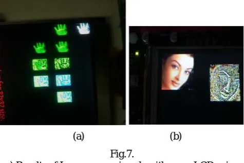
The resulted images after image processing are shown in Figure 6. By thresholding technique the 32x32 image is generated as binary image. These resulted images are also displayed on the LCD screen of the PIC32 interfacing kit in real-time for researchers’ visual inspection.
(a) (b) Fig.7.
a) Results of Image processing algorithms on LCD using PIC32 microcontroller for 32 x32 size images for palm. b) Edge detected image of size 90x90 on LCD for human
face
Above methods are used to expose salient features of an image in small size and 32x32 in binary form. Above image processing operations such as Gaussian filter, laplacian filter are windowing operations where a weighted moving operation is performed on a small window of pixels.
Due to computational complexity in the windowing operations, simple Pixel wise operations are concerned to achieve high data rate. Pixel-wise image-processing operations modify a pixel’s intensity (brightness) value x
independent of the values at other pixels.
When we want to change the brightness of any light source, one thing we need to consider is how humans perceive the brightness. Human eye perceives the brightness change non-linearly. We have better sensitivity at low luminance than high luminance i.e in light source we see big brightness change between low luminance input 1 and 2. We don’t see brightness change between high luminance input 244 and 255. In Pixel-wise operations, to control light source brightness linearly to human eye, a real-valued function f(x) is used to adjust a pixel’s brightness value x independent of the values at other pixels. Gamma correction (image enhancement technique) is used to compensate for non-linearities in recording or display devices, or to increase pixel contrast. To evaluate the image processing algorithms for retinal prosthesis, some experiments have been carried out in Matlab platform and Microcontroller IDE. These algorithms are evaluated by emulation on PIC32 microcontroller under normal and dark room lighting conditions.The 256x256 size RGB input from OV9650 Camera and the processed 6 bit 32x32 size image output on LCD is shown in Figure 7.
C. Image Encoding
The processed single colored pixel values are encoded into picture data frame according to the synchronous data communication protocol shown in figure 8.
Fig.8. Image Processing input and output recorded on LCD.
Each data frame starts with one sync character as 7E Hex (Frame Cycle Synchronous Byte (FCSB)) followed by 1024-bytes corresponding to 1024 electrode charge values which represent image’s brightness.
Fig.9. Picture data frame format for wireless transmission For all electrodes/pixels channels in the electrode array, electrode stimulation parameters of a electrode stimulation signal (bi-phasic current pulse) such as pulse amplitude, pulse polarity, inter phase gap between pulses, pulse repetition rate (stimulation rate) are same. The encoded
picture/ pixel data frames are serially transmitted to ASK modulated RF transmitter through transmit pin (U2Tx) of UART peripheral module of the PIC32.
D. Image transmission to RIRS
For dispatching data to ASK modulated RF transmitter, there is a need for better and efficient method for transmitting serial data. To transmit data serially to other devices at faster rates and with less circuitry, the high-level protocols such as UART, SPI, CAN, I2C. etc.. are available in PIC32. UART is preferred than SPI, I2C because their slave devices are need separate clock line initialized by master device. UART is preferred because of minimized size constraint of retinal implant. The UART uses standard non-return-to-zero (NRZ) format (one Start bit, eight or nine data bits, and one or two Stop bits). It supports Full-duplex, 8-bit or 9-bit data transmission, hardware auto-baud feature and Parity support. . The data format used for serial transmission is 8 bits, no parity, and one Stop bit (denoted as 8, N, 1).
The encoded image data bytes are serially transmitted to ASK modulator through UART transmit pin. ASK modulation is used for data telemetry in our work due to its simplest design, low power consumption and low cost. In this paper the ASK modulator will be presented with
frequency 1MHZ and efficient class-E power amplifier operated with carrier frequency 8.195MHZ to avoid the tissue damage according to the industrial scientific medical (ISM) band [5], with modulation index 11.1% to achieve 1Mbit/s for the external part.
IV. EXPERIMENTAL RESULTS
Visual inspection is an intuitive way to observe the operation of the system. Two methods are implemented in this prototype for real-time output verification: a 256-channel LED array, and a pseudo 256-channel LED.
A. Pseudo channel LCD
Pseudo channel is built with a Microcontroller based LCD in conjunction with custom software running on a laptop computer. The digital signal carrying the stimulation parameters for all 1024 channels is tapped out on LCD at transmitter side. There are several advantages in using this pseudo channel. It provides a real-time visual feedback of the system operation status.
B. LED Array:
In EIPS, the encoded data to be transmitted from EIPS to RIRS through wireless transcutaneous link is verified with 32x32 LED array. Visual inspection is an intuitive way to observe the operation of the system. The LED array, which directly connects to the EIPS output to provide visual feedback.
The output on LED array should be dot-by-dot identical to the transmitted image on the LCD, so any malfunction in transmission of pixel data can be easily detected. It is worth FCSB EC1 EC2 EC3 EC 4 - -
-
EC 1023 EC 1024
1024-bytes of Electrode Charge (EC) information corresponding to pixel brightness Sync
Byte
Sharmili N et al, / (IJCSIT) International Journal of Computer Science and Information Technologies, Vol. 6 (2) , 2015, 1134-1140
Fig.10. System operation can be easily monitored with real-time visual feedback on the computer screens and the 1024-channel LED array. The first column is the image captured in 256x256 size, the second column is resized image of 32x32 size in RGB and green color formats and the third column is captured from the LED array using a still camera
noting that these pictures which are shown in first column are recorded in SD Card with camera freezing, a useful debugging feature designed in the transmitter software which stops the camera from snapping new pictures and repeatedly sends out the last captured image. The software on the EIPS transmits those images continuously is also a good platform to verify the functionality of EIPS before it is fabricated as IC which modulates the incoming picture data bytes and transmits to RIRS through wireless telemetry at 1Mbps bit rate.
All these tasks are developed with emulation software of PIC32 based SSD1928 Evaluation Kit (SSD1928 EK) and debugging is done on a laptop computer. High-level computer programming languages and a user friendly debugging environment of MPLAB IDE for PIC32 greatly increase the efficiency of algorithm implementation and testing.
V. CONCLUSION
A microcontroller based real-time research platform for Epiretinal Prosthesis has been developed with the main image processor Microchip’s PIC32 microcontroller on Techtoys SSD1928 evaluation kit at transmitter side. The system has been tested by using captured image data in real time and verified using 16x16 and 32x32 resolution LCD/LED array with satisfactory results which are shown in figure 6. The major advantage of using a PIC32 based SSD1928 EK and computer provides the flexibility of evaluating various algorithms in real time and can be powered (3.7V 2700mAH Li-Ion) through battery. With the technology improvements nowadays microcontrollers with inbuilt peripherals and graphics features are available in 8
pin package with small size (Ex: NXP products ...etc.). So EIPS modules can be integrated and implemented in a manner similar to Android Apps in any portable device like iPhone where PIC32 microcontroller or any processor is used. The proposed experimental retinal prosthesis can be utilized in the development of the next generation of higher density retinal prosthetic with minimal hardware and software changes to go through more demanding image processing algorithms. The presented results would encourage researchers to use this platform for their future work.
REFERENCES
[1] Banarji, A., V. S. Gurunadh, S. Patyal, T. S. Ahluwalia, D. P. Vats, and M. Bhadauria, "Visual prosthesis: Artificial vision," Medical
Journal Armed Forces India 65, no. 4, pp. 348-352, 2009.
[2] S. K. Kelly, et al., "Realization of a 15-channel, hermetically-encased wireless subretinal prosthesis for the blind," in Engineering in Medicine and Biology Society, Annual InternationalConference of
the IEEE, pp. 200-203, 2009.
[3] L. H. Jung, N. Shany, T. Lehmann, P. Preston, N. H. Lovell, and G. J.Suaning, “Towards a chip scale neurostimulator: System architecture of a current-driven 98 channel neurostimulator via a two-wire interface,”inProc. IEEE Eng. Medicine and Biology Conf., pp.6737–40, Aug. 2011.
[4] J. D. Weiland, W. Liu, and M. S. Humayun, "RETINALPROSTHESIS," Annual Review of Biomedical
Engineering, vol. 7, pp.361-401, 2005.
[5] N. Tran, J. Yang, S. Bai, D. Ng, M. Halpern, D. B. Grayden, E.Skafidas, and I. Mareels, "A fully flexible stimulator using 65 nm cmos process for 1024-electrode epi-retinal prosthesis," in
Engineering in Medicine and Biology Society, 2009. EMBC 2009.
Annual International Conference of the IEEE, pp. 1643-1646, 2009,.
[6] Niu, JinHai, YiFei Liu, QiuShiRen, Yang Zhou, Ye Zhou, and ShuaiNiu. "Vision implants: An electrical device will bring light to the blind." Science in China Series F: Information Sciences 51, no. 1 , pp. 101-110,2008.
[7] N. Tran, E. Skafidas, J. Yang, S. Bai, M. Fu, D. Ng, M. Halpern, and I. Mareels. "A prototype 64-electrode stimulator in 65 nm CMOS process towards a high density epi-retinal prosthesis." In Engineering in Medicine and Biology Society, EMBC, 2011 Annual International Conference of the IEEE, pp. 6729-6732. IEEE, 2011. [8] K. Ganesan, A. Stacey, H. Meffin, S. Lichter, U. Greferath, E. L.
Fletcher, and S. Prawer. "Diamond penetrating electrode array for epi-retinal prosthesis." In Engineering in Medicine and Biology Society (EMBC), 2010 Annual International Conference of the IEEE, pp. 6757-6760. IEEE, 2010.
[9] K. Chen, Y.K. Lo, Z. Yang, JD.Weiland, M.S. Humayun, and W. Liu, “A System Verification Platformfor High-Density Epiretinal Prostheses,” IEEE Transaction on Biomedical Circuits and System, Volume 7,Issue 3, pages 326-337 (12pp), 2013.
[10] G.Wang, P.Wang, Y. Tang, and W. Liu, “Analysis of dual band power and data telemetry for biomedical implants,” IEEE Trans.
Biomed. Circuits Syst., vol. 6, no. 3, pp. 208–215, Jun. 2012..
[11] Omni Vision OV9650 Color CMOS SXGA 1.3Mega Pixel Camera Chip, http://www.techtoys.com.hk/
[12] Matteucci, B. Paul , Philip Byrnes-Preston, Spencer C. Chen, H. Lovell, and Gregg J. Suaning. "ARM-based visual processing system for prosthetic vision." In Engineering in Medicine and Biology Society, EMBC, 2011 Annual International Conference of
the IEEE, pp. 3921-3924. IEEE, 2011.
[13] PIC32 microcontrollers datasheet: Available at www.microchip.com/downloads/en/DeviceDoc/61143E.pdf
[14] SSD1928 Data sheet Available at www.solomon-systech.com/pdf/AppNote_SSD1928_10.pdf.