Abstract— This paper presents a methodology to reduce the area of DSP architecture on silicon using folding. Folding is particularly important and has impact on large DSP circuits/architectures. This technique is powerful to reduce functional units in DSP circuits/architectures which mainly depend on folding factor. The folding technique is used to derive the control circuitry of the hardware architectures such as functional units (adders and multipliers). Folding technique also supports complex operations with time multiplexing. The time multiplexing reduces the area by repeating computations on the same hardware unit. Apart from folding technique, register minimization technique is used to minimize the number of registers. This methodology is verified using Spartan 3A/3AN device family. The comparison table of unfolded and folded circuits shows the better performance of the folding algorithm.
Index Terms: DFG, folding, foldingfactor, DSP, retiming, Lifetime analysis.
I. INTRODUCTION
The widespread use of digital representation of signals for transmission and storage has created challenges in the area of digital signal processing (DSP). In response to these challenges, DSP techniques have emerged for tasks such as area reduction and power reduction [1]. DSP is used in numerous applications such as video compression, modems, multimedia, speech processing and biomedical signal processing. The field of DSP has always been driven by the advances in DSP applications and in VLSI technologies.
These implementations are required to satisfy the enforced sampling rate constraints of the real time DSP applications and use less space and power consumption. DSP computation is different from general purpose computation in the sense that the DSP programs are nonterminating programs. In DSP computation the same program is executed repetitively on an infinite time series. The nonterminating nature can be exploited to design more efficient DSP systems by exploiting the dependency of tasks both within iteration and among multiple iterations. These algorithms need to be modified for the design of low speed or low area implementations. In DSP architectures it is important to minimize the silicon area of the integrated circuits, which is achieved by reducing the number of functional units such as adders and multipliers. The process of executing many algorithm operations in one hardware operator is referred to as folding [2]. The folding technique is used to determine the control circuits in DSP architectures where multiple algorithm operations are time multiplexed to a
single functional unit such as a pipelined adder [4], [5]. By executing multiple algorithm operations on a single functional unit, the number of functional units in the implementation is reduced, resulting in smaller silicon area. Folding technique can also be used for synthesis of DSP architectures that can be operated using single or multiple clocks.
The folding technique can be used in any of the DSP architectures where there is a requirement of substantial area reduction. Folding provides a means of trading area for time in DSP architectures. Folding equations can be used to systematically determine the control circuitry for the architecture from a data flow graph. Folding can also be used to address other related problems in high-level synthesis in a formal manner.
The paper is organized as follows. Section II reviews some fundamentals of data flow graphs. Section III derives the folding equations which are used to synthesize the control circuits for the DSP architectures. Register minimization is addressed in the section IV. In section V synthesis results are given. Conclusions are stated in section VI.
II. DATAFLOW GRAPHS
Data flow graphs (DFGs) are used in the simulation of computer systems. The main advantage of data flow graphs over other models of parallel processors is their compactness and general amenability for direct interpretation. That is, the translation from the conceived system to a DFG is straight-forward and, once accomplished, it is equally straightstraight-forward to determine by inspection which represent the aspects of the system. Because of the hierarchical nature and the modularity of data flow graphs, both software tasks and hardware units can be modeled using DFGs [9], [11-13].
The tasks of the DSP algorithm are assumed to be executed repetitively. Each node in the DFG represents an algorithm operation or task, and any arc U → V withi delay (where i is any nonnegative integer) implies that the result of ith iteration of U is used to execute the (l+ i)th iteration of V. The arcs with delays dictate the inter-iteration precedence constraints, whereas the arcs without delays represent the intra-iteration precedence constraints. The folded hardware architecture is also described by hardware DFG. In the hardware DFG, HU,
denotes the hardware operator that executes the operation U as shown in figure 1. All operations processed by HU, collectively
form an ordered set S, where the ordering of the elements represents a unique execution sequence of the tasks in the folded operator. Some operations in set S can be null Rakhi S1, PremanandaB.S2, Mihir Narayan Mohanty3
1
Atria Institute of Technology, 2East Point College of Engineering &Technology, Bangalore., 3ITER, Siksha „O‟ Anusandhan University, Bhubaneswar.
.
Synthesis of DSP Systems using Data Flow Graphs
for Silicon Area Reduction
operations denoted as Φ. N represents the folding factor which is an important factor in folding. If Nurepresents the number of
operations in S,then the ordering of the operations ranges from 0 to Nu - 1 and each execution order number corresponds
directly to a time partition. Let PUdenote the level of pipelining
of the hardware operator HU. The objective is to fold the
original DFG for a specified folding set to obtain the hardware architecture DFG. Interprocessor communication links and the storage units required in these links are also obtained. A delay or register in the hardware DFG represents a storage unit.
III. DERIVATION OF FOLDING EQUATIONS
Folding is a technique for determining control circuits in architectures where multiple algorithm operations (such as addition operations) are time-multiplexed to a single hardware module (such as a pipelined ripple-carry adder) [2]. Folding equations have been derived in the past for folding single-rate algorithms to rate architectures, and for folding single-rate algorithms to multisingle-rate architectures [3]. The basic concepts behind using folding to synthesize control circuits for time multiplexed architectures are the same for single-rate folding and multi-rate folding. The two extremes of this are when a fully parallel implementation is used (i.e., each algorithm operation is assigned its own functional unit in hardware) and when a single processor is used (i.e., the entire program is implemented on a single functional unit).
Consider an arc (also referred to as an edge) connecting U and V nodes and with i delays (iD), as in Fig. 1 (a). Let the lth iteration of nodes U and V be scheduled to execute at time NUl+u units and NV+v, respectively, where u and v are the
folding orders of nodes and which satisfy u[0, NU] and v[0, NV].
The hardware operators (also referred to as functional units) which execute nodes U and V are denoted as HU and HV
respectively. NU and NV (number of operations) are folded to
HU and HV respectively. If HU is pipelined by PU stages [10],
then the result of the l thiteration of node U is available at NUl+u+PU. .Since arc U→V has i or (w(e)) delays, the result of
node is used by the (l+i)th iteration of which is executed at NV(l+i)+v.
Therefore, the result must be stored for DF(U→V)= NV(l+i)+v-(NUl+u+PU)
=( NV-NU)l+ NVi- PU+v-u (1)
time units. Since it is assumed that DSP programs iterate from l=0 to l=∞, practical concerns require NV=NU to avoid the cases
where DF(U→V) approaches +∞ or -∞ or as gets large. With
N= NV=NU the folding equation becomes
DF (U→V) =Ni- PU+v-u (2)
which is independent of the iteration number l. Arc U→V maps to a path from HU to HV in the architecture with DF(U→V)
delays, and data on this path are input to HV at Nl+v as
illustrated in Fig. 1(b).
A folding set is an ordered set of N operations executed by the same functional unit. The operations are ordered from 0 to N-1. Some of the operations may be null. For example, Folding set S1={A1,0,A2} is for folding order N=3. A1 has a folding order of 0 and A2 of 2 and are respectively denoted by (S1|0) and (S2|2). For a folded system to be realizable, DF(U→V) ≥ 0
must hold good for all of the edges in the DFG. Once valid folding sets have been assigned, retiming can be used to either satisfy this property of determine that the folding sets are not feasible.
Folding technique is explained by considering the example of an IIR Filter. Consider a Biquad filter shown in Fig. 2 with the corresponding folding sets [8]. A Biquad filter is a second order infinite impulse response (IIR) filter which is widely used in DSP applications. It is a recursive filter which contains two poles and two zeros. The output of a Biquad filter depends on past outputs as well as past inputs. The folding equations for each edge are given in the Table I using equation (2). Retiming has to be performed before folding to force causality to the system. Retiming is a transformation technique used to change the locations of delay elements in a circuit without affecting the input/output characteristics of the circuit [7].
Fig. 2: DFG of Biquad Filter.
Retiming is characterized by retiming values for each node in the DFG. Retiming only affects the weights of the edges. It is basically adding and removing delays on the edges.
TABLE I
Folding Equations and Retiming for folding Constraints Edge Folding Equation Retiming for folding
Constraints
1→2 DF(1→2) =-3 r(1)-r(2)≤-1
1→5 DF (1→5)= 0 r(1)-r(5)≤0
1→6 DF (1→6)= 2 r(1)-r(6)≤0
1→7 DF (1→7)= 7 r(1)-r(7)≤-1
1→8 DF (1→8)= 5 r(1)-r(8)≤1
3→1 DF(3→1) = 0 r(3)-r(1)≤0
4→2 DF (4→2)= 0 r(4)-r(2)≤0
5→3 DF (5→3)= 0 r(5)-r(3)≤0
6→4 DF (6→4)=-4 r(6)-r(4)≤-1
7→3 DF (7→3)=-3 r(7)-r(3)≤1
8→4 DF(8→4) =-3 r(8)-r(4)≤-1
Using retiming, the number of delays on the edge U→V is changed from w(e) to wr(e) .
wr (e) =i′= w(e)+r(V)-r(U) (3)
where wr(e) or i′ is the number of delays on the edgeU→V in
the retimed DFG, and r(V) and r(U) denotes the retiming value of the node U and V respectively.
Let D′F(U→V) denote the number of folded delays
obtained by folding the edge U→V in the retimed DFG. Ensuring the corresponding edge in the folded hardware has a nonnegative number of delays, the constraint D′F(U→V)≥0
must hold good, implies that,
Ni′- PU+v-u ≥0 (4)
Substituting DF(U→V) from (2) and solving for r(U) - r(V)
results in,
r(U)-r(V) ≤ D(U→V) (5) N
Since the retiming values of the nodes are restricted to be integers, this can be rewritten as,
(6)
which gives the floor value, which is the largest integer less than or equal to the difference value.
Fig. 3: Constraint Graph.
The set of constraints for the DFG is found using constraint graph shown in Fig. 3. There is one such constraint, represented as an inequality in Table I for each edge in the DFG. The system of inequalities can be solved using Bellman-Ford algorithm [11]. Using the Bellman Bellman-Ford algorithm, it is found that the set of constraints has a solution, and one such solution is r(1)=-1, r(2)=0, r(3)=-1, r(4)=0, r(5)=-1, r(6)=-1, r(7)=-2, r(8)=-1. Using these new retimed values we can find new delay between edges using equation (3). Now apply the
folding equation (4) to find the new delays from which folded architecture can be derived from it.
IV.
R
EGISTERM
INIMIZATIONMinimizing the number of registers in DSP architecture is important results in the reduction of silicon area. The folded structure contains more number of registers because the intermediate results needs to be stored. A data sample (variable) is live from the time it is produced till it is consumed. After the sample is consumed, it is dead. A variable occupies one register when it is live. In Lifetime analysis, the number of live variables at any time unit is determined, which gives the minimum number of registers required to implement the DSP program.
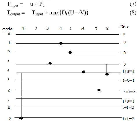
A linear lifetime chart shown in Fig. 4 is used to graphically represent the lifetime of each variable in a linear fashion. In a linier lifetime chart horizontal lines represent clock cycles and the vertical lines present lifetimes clock cycle in which it is consumed. The maximum number of live variables at any time step is 2, so the minimum number of registers that can be used to implement the architecture is 2.
The lifetime analysis begins with the construction of a lifetime table. It uses a matrix transpose operation. We need to construct a table with Tinput and Toutput. Tinput is the time unit in
which the node produces the data Toutput is the latest time that
the result of the node is used.
Tinput = u + Pu (7)
Toutput = Tinput + max{DF(U→V)} (8)
Fig. 4: A linear lifetime chart for the Biquad filter.
The lifetime chart uses the convention that a variable is not live during the clock cycle in which it is produced, which is the output time of the variable ignoring the latency of the system. Once the lifetime table is obtained a life time chart is created. During this the periodicity of the circuit needs to be considered. After this the number of live variables present in each cycle is calculated which gives the minimum number of register required in the folded architecture which is 2 in this case. Using this, folded architecture which uses minimum registers is derived and is shown in Fig. 5.
Fig. 5: Folded Biquad Filter with two registers.
V.
S
YNTHESISR
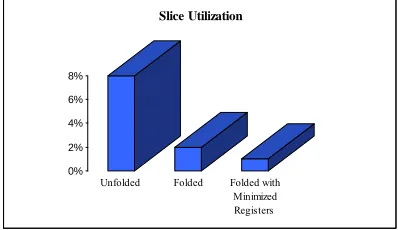
ESULTSThe architectures of unfolded, folded and with minimum registers are synthesized in Spartan-3A/3AN device family. Spartan FPGA contains basic resources such as slices, IOBs (I/O blocks), LUTs (look up tables) and interconnects. Each Spartan FPGA slice contains two 4-input LUTs and two flip-flops. The area utilization of a circuit in FPGA depends on mainly number of occupied slices and 4-input LUTs. The comparison of the results is shown in Table II and III respectively.
A graph representing the slice utilization of three architectures is shown in Fig. 6. The unfolded architecture gives a slice utilization of 8%. But when the folding is performed it reduces to 2% because of the reduction of functional units. For this architecture when we perform register minimization, the number of register required will get reduced.
TABLE II Summary of Device Utilization
Architecture Unfolded Folded Folded with min.
registers
# of Slices 60 18 14
# of LUTs 100 8 8
# of Slice FFs 32 32 24
TABLE III
Percentage (%) of Device Utilization
Architecture Unfolded Folded Folded with min.
registers
# of Slices 8 2 1
#of LUTs 7 0(.0056) 0(.0056)
# of Slice FFs 2 2 1
The synthesis report of the third architecture will give a utilization of 1% which is significantly less compared to the first architecture.
0% 2% 4% 6% 8%
Unfolded Folded Folded with Minimized Registers
Slice Utilization
Fig. 6: Comparison of Slice Utilization.
VI.
C
ONCLUSIONProgress has been made towards the reduction of area using process technology. Here a methodology is proposed which can reduce the functional units in the design phase of DSP architectures. The methodology described above can be fully automated in Matlab to get a better circuit, especially in VLSI-DSP area to minimize the silicon area. Also different architectures are synthesized and the device utilization is compared. Further studies can be taken on implementing this technique for multirate systems.
REFERENCES
[1] Dejan Markovic, Borivoje Nikolic, Robert W. Brodersen, “Power and Area Efficient VLSI Architectures for communication Signal processing”, Berkeley Wireless Research Center, University of California at Berkeley.
[2] Parhi K.K, Wang. C.Y, Brown A. P, “Synthesis of control circuits in folded pipelined DSP architectures”, IEEE Journal of Solid-State Circuits, Volume 27, Jan 1992, pp. 29 – 43.
[3] Denk T.C, Parhi K.K “Synthesis of folded pipelined architectures for multirate DSP algorithms”, IEEE Transactions on Very Large Scale Integration (VLSI) Systems, Volume 6, Dec 1998, pp. 595 – 607.
[4] Rajopadhye S, Kiaei, S “A folding transformation for VLSI IIR filter array design, International Conference on Acoustics, Speech, and Signal Processing, Volume 2, 1991, pp. 1237-1240 .
[5] Keshab K Parhi, “VLSI Digital Signal Processing systems – Design & implementations”, John Wiley & Sons, Inc.
[6] K. K. Parhi, “Algorithm transformation techniques for concurrent processors”, Proc. IEEE (Special Issue on Supercomputer Technology), Dec 1989, pp.1879–1895. [7] C. Leiserson, F. Rose, and J Saxe, Optimizing Synchronous circuitry by retiming,” in Third Caltech Conf. VLSI, pp.87-116, 1983.
[8] L. B. Jackson, J.F. Kaiser, and H.S. McDonald,” An approach to implementation of digital filters” IEEE Trans. Audio Electroacoust. Vol.AE-16, no.3, pp.413. [9] Edward Ashford Lee, “Consistency in Data Flow
Graph”, IEEE transactions on parallel and distributed systems, vol 2, pp.223-235, 1991.
[10] Parhi K.K, Wang., “Automatic generation of control circuits in pipelined DSP architectures”, in Proc. IEEE Int.Conf.Computer Design,sept.1990, pp. 324 – 327. [11] Boros, E. Hammer, P. L. Shamir, R. Rutgers Univ.,
New Brunswick, NJ, “A polynomial algorithm for balancing acyclic data flow graphs,” IEEE Transactions, vol. 41, pp. 1380–1385, 1992.
[12] Edward Ashford Lee,” Consistency in Data Flow Graph”, IEEE transactions on parallel and distributed systems, vol 2, pp.223 235, 1991.
[13] J. L. Gaudiot and M.D.Ercegovac, "Performance analysis of data flow computers with variable resolution actors," in Proc. 4th Int.Conf. Distrib. Comput. Syst., San Francisco, CA, May 1984, pp. 2-9.