Design & Implementation 8-Bit Wallace Tree
Multiplier
Bhupender Pratap Singh1, Rakesh Kumar2
M.Tech Scholar[VLSI Design], Dept. of ECE, Sobhasaria Engineering College, Sikar, Rajasthan, India1
Assistant Professor, Dept. of ECE, Sobhasaria Engineering College, Sikar, Rajasthan, India 2
ABSTRACT :- Many multipliers that are of high-speed, low power and standard in design are used in multiplication process. Numerous efforts have been used to decrease the number of partial products generated in a multiplication process. One of the efforts is Wallace tree multiplier. This work aims at designing and implementation of 8 bit Wallace tree multiplier using VHDL language. A Wallace tree multiplier is an upgraded version of tree based multiplier architecture. Wallace tree multiplier use carry save addition algorithm to decrease the latency. Speed of Wallace tree multiplier can be improved by using compressor methods. By minimizing the number of partial products we used half adder and full adder in 8 bit multiplier. In this Wallace tree multiplication process we also used carry save adder in the last stage to accumulate the last bits. In this work 8*8 bit Wallace tree multiplier construction is examined and simulated in XILINX software. To implementation and simulation of 16 bit Wallace tree multiplier we used XILINX ISE Design suite 14.6 software. In this 8 bit Wallace tree multiplier circuit our main goals are to decrease the area of multiplier circuit and increase the speed of multiplier.
KEY WORDS:- 8-bit Wallace tree, VHDL Language, Xilinx 14.6 Design Suit Software
I.INTRODUCTION
Multiplier plays an important role in today’s digital signal processing and diversity of other applications. There are many multiplier are used in the digital signal processing system like binary multiplier, tree multiplier, Array multiplier etc. With advances in technology, a lot of researchers have tried and are trying to design multipliers which recommend any of the following design targets – high speed, low power utilization, regularity of layout and hence minimum area or even combination of them in one multiplier therefore making them suitable for a variety of high speed, low power and dense VLSI implementation. Multiplication of two binary numbers is fundamental and most frequently used arithmetic operations. Statics shows that more than 70% instructions in microprocessor and mainly DSP algorithms perform addition and multiplication [1][2]. High speed is main issue to design a multiplier for a designer. The speed of a multiplier determines its performance. High speed multiplier is an essential requirement for all multiplication methods. Low power utilization is also a main topic in multiplier design. To decrease major power utilization it is good to decrease the number of operation by this means decreasing dynamic power which is a main part of total power utilization so the need of high speed and low power multiplier has increased. Designer mainly focuses on high speed and low power efficient circuit design. The purpose of a good multiplier is to provide a physically packed together, high speed and low power utilization unit.
metrics.[3]
II.METHODOLOGY
A Wallace treeis a very useful hardware function that is used in digital circuit for multiplies two integers. In Wallace method the multiplication of two numbers is done by reducing the partial product matrix into a two-row matrix by a half adder, full adder, carry-save adder & these two rows are added utilizing a fast carry propagate adder to produce the output product. In this Wallace tree method we used half adder for summation of 2 bit and used full adder for summation of 3 bit. For multiplicands of higher than 8-bits this advantage is more beneficial, because the addition of partial products is low in Wallace tree and hence increases speed. Here each bit of each partial product in every column is added together by a set of counters used in parallel so that no carry is propagated further. Then this matrix is reduced by another set of counters until a two-row matrix generates. [4][5]
Fig.1 Multiplication of 8 bit Wallace tree [6] Fig.2 Representation of Half adder & Full adder
full adder and 2 half adder where are we used some Sum signal S17 to S32 and Carry signal C17 to C32. In the next stage we used 7 full adder and 4 half adder where we used Sum signal S43 to S53 and Carry signal C43 to C53. In the next stage we used carry save adder and there are we used 2 half adder and 9 full adder to reduce this stage and we find out the output result.
After complete the programing of 8 bit Wallace tree we used the Xilinx 14.6 design suit software. In this Xilinx software we write the all programme and implement this programme. When we implement the all programme and then we see the RTL view of 8 bit Wallace tree. After checking the RTL view of this programing then we simulate this programing and check the waveforms. In this simulation process we give an input of A & B and we get the output of all Sum Signal, Carry signal and X output Signal.
III.RESULT & DISCUSSION
In this multiplication process first we implement the programme in Xilinx Software then we see the RTL view of this 8 bit Wallace tree multiplication process. In this RTL view we see the interconnection of half adder and full adder with Sum and Carry signal.
Fig.3 RTL view of 8 bit Wallace tree Fig. 4 Internal block diagram of RTL view
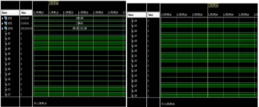
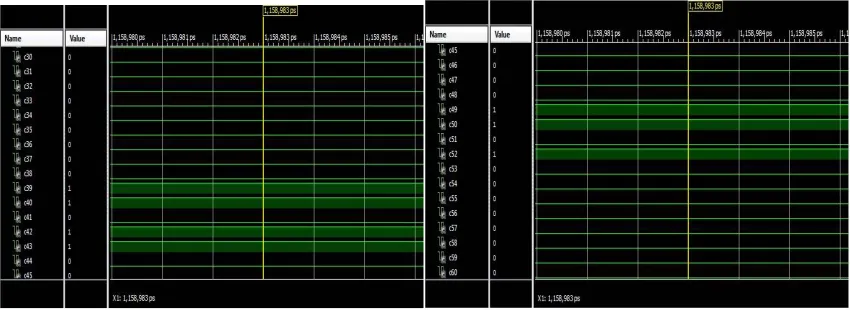
When we simulate this programing in Xilinx software then we give the input value of A & B, then we run the programme and we get the all Sum signal, Carry signal and X output signal. In this we get all result in graphical form. So all results are given in graphical form
Input A: - 10101100 B: - 11100101 So output X is given by
X: - 1001100111011100
Fig. 5 Snapshot of Simulation Result Part 1 Fig. 6 Snapshot of Simulation Result Part 2
Fig. 7 Snapshot of Simulation Result Part 3 Fig. 8 Snapshot of Simulation Result Part 4
Fig. 11 Snapshot of Simulation Result Part 7 Fig. 12 Snapshot of Simulation Result Part 8
Fig. 13 Snapshot of Simulation Result Part 9
IV. CONCLUSION
This paper offers the multiplication process of 8 bit using Wallace tree. In this work we used VHDL structural type programing language to multiply the 8 unsigned bits. In this 8 bit Wallace tree multiplication process, we used half adder, full adder & carry save adder to reduce the bit in the multiplication process. In this Wallace tree multiplication process, we used five stages to reduce all the bits. We are going to use Xilinx 14.6 Ise design suite software for implementation and simulation of this multiplication process. In the implementation of Wallace tree multiplication process, we got an output image of RTL view. In the simulation process, we got an output graphical images of all input, output and signal value.
REFERENCES
[1] Kai Hwang “Computer Arithmetic: Principles, Architecture, and Design” John Wiley & Sons 1979
[2] S. D. Pezaris "A 40-ns 17-Bit by 17-Bit Array Multiplier", IEEE Trans. on Computers, pp. 442-447,.Apr. 1971
[3] C. Baugh y A. Wooley "A Two's Complement Parallel Array Multiplication Algorithm". IEEE Trans.on Computer, Vol.C-22, Nº12. Dec.1973.
[4] Weste, Neil H.E. Eshraghian, and kamran,” CMOS VLSI Design: A Circuit and System Prespective”, 3rd Edition, Pearson Education, pp.
345-356, 2005.
[5] Neeta Sharma, Ravi Sindal “Modified Booth Multiplier using Wallace Structure and Efficient Carry Select Adder”,International Journal of Computer Applications (0975 – 8887) Volume 68– No.13, pp 40-42,April 2013.
BIOGRAPHY
Mr. BHUPENDER PRATAP SINGH
Bhupender Pratap Singh was born in Udaipur Distt. (Rajasthan) India in 1986. He has completed his Engineering in 2008 from Kautilya Institute of engineering & Technology, Jaipur (Rajasthan), India. He is M.Tech Research Scholar (VLSI Design) in Sobhasaria Engineering College, Sikar(Rajasthan), India, affiliated to Rajasthan Technical University, Kota(Rajasthan),India.