A Five Level Space Vector Pulse Width Amplitude
Modulation for a Buck-Boost Voltage Source Inverter
K. Jagdishwarji
P1
P
, Mondi Vinod Kmar
P2
P
, Dr. S. Siva prasad
P3
P
1
P
M.Tech student (EPS), JB Institute of Engineering and Technology (UGC Autonomous) , Hyderabad. Email:
32TU
[email protected]
U32TP
2
P
Assoc Prof, Dept of EEE, J.B Institute of Engineering and Technology (UGC Autonomous), Hyderabad,
E-mail:
U[email protected]
P
3
P
Professor & HOD, EEE Dept., JB Institute of Engineering and Technology (UGC Autonomous), Hyderabad.
Email:
32TU[email protected]
U32TAbstract-
This paper proposes a space vector pulse width amplitude modulation (SVPWAM) method for a buck–boost voltage/current source inverter. Multilevel voltage-fed inverters with space vector pulse width modulation strategy are gained importance in high power high performance industrial drive applications. Multi-phase machines and drives is a topic of growing relevance in recent years, and it presents many challenging issues that still need further research. In this paper a 5-level SVPWAM is proposed which is having better features than the conventional 2-level SVPWAM. All the simulations are carried out in MATLAB/Simulink software environment.Keywords
: Buck-boost, SVPWAM, 2-level, 5-level,switching loss reduction, THD.
1. Introduction
The need for increased power level ac drive systems in place of conventional two-level inverter configuration is the main requirement of the present days. The standard two-level voltage source inverter is composed of only one switch cell per phase. But in the field of high power driving systems the level of dc current bus voltage constitutes an important limitation of the handled power. Another drawback of the two-level converter is very high dv/dt generated by two-level voltage source inverter. More over as the dc-link voltage of a two-level inverter is limited by voltage ratings of switching devices, the problematic series connection of switching devices is required to raise the dc link voltage. By this the maximum allowable switching frequency has to be more lowered thereby harmonic reduction becomes more difficult. Hence the need for high performance ac drive systems, at increased power level high quality inverter output with low harmonic loss and torque pulsation has arisen. Multi-level converters come as a solution to these problems. Their performance depends on the PWM method that is used.
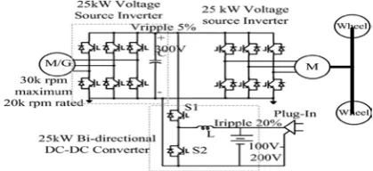
Currently, two existing inverter topologies are used for hybrid electric vehicles (HEVs) and electric vehicles (EVs): the conventional three-phase inverter with a high voltage battery and a three-phase pulse width modulation (PWM) inverter with a dc/dc boost front end. The conventional PWM inverter imposes high stress on
switching devices and motor thus limits the motor’s constant power speed range (CPSR), which can be alleviated through the dc–dc boosted PWM inverter.
Fig. 1 shows a typical configuration of the series plug-in electric vehicle (PHEV). The inverter is required to inject low harmonic current to the motor, in order to reduce the winding loss and core loss. For this purpose, the switching frequency of the inverter is designed within a high range from 15 to 20 kHz, resulting in the switching loss increase in switching device and also the core loss increase in the motor stator. To solve this problem, various soft-switching methods have been proposed [1]– [3]. Active switching rectifier or a diode rectifier with small DC link capacitor have been proposed in [4], [5], [8]–[12]. Varies types of modulation method have been proposed previously such as optimized pulse-width-modulation [13], improved Space-Vector-PWM control for different optimization targets and applications [14]– [16], and discontinuous PWM (DPWM) [17]. Different switching sequence arrangement can also affect the harmonics, power loss and voltage/current ripples [18]. DPWM has been widely used to reduce the switching frequency, by selecting only one zero vector in one sector. It results in 50% switching frequency reduction. However, if an equal output THD is required, DPWM cannot reduce switching loss than SPWM. Moreover, it will worsen the device heat transfer because the temperature variation. A double 120 flattop modulation method has been proposed in [6] and [7] to reduce the period of PWM switching to only 1/3 of the whole fundamental period. However, these papers did not compare the spectrum of this method with others, which is not fair. In addition, the method is only specified to a fixed topology, which cannot be applied widely.
Fig. 1 Typical configuration of a series PHEV This paper proposes a novel generalized space vector pulse width amplitude modulation (SVPWAM) method
for the buck/boost five level voltage source inverter (VSI). In this paper a new simplified, very efficient multi-level SVM method for five-level diode clamped inverter and three-level diode clamped inverter is developed using simulink block sets of MATLAB and this algorithm is used to generate gating pulses for multi-level inverters and also the performance of the three induction motor is studied based on the developed algorithm.
2. SVPWAM FOR VSI
A. Principle of SVPWAM Control in VSI
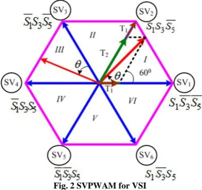
The principle of an SVPWAM control is to eliminate the zero vector in each sector. The modulation principle of SVPWAM is shown in Fig. 2. In each sector, only one phase leg is doing PWM switching; thus, the switching frequency is reduced by two-third. This imposes zero switching for one phase leg in the adjacent two sectors.
Fig. 2 SVPWAM for VSI
For example, in sector VI and I, phase leg A has no switching at all. The dc-link voltage thus is directly generated from the output line-to-line voltage. In sector I, no zero vector is selected. Therefore, S1 and S2 keep constant ON, and S3 and S6 are doing PWM switching. As a result, if the output voltage is kept at the normal three-phase sinusoidal voltage, the dc-link voltage should be equal to line-to-line voltage Vac at this time Consequently, the dc-link voltage should present a 6ω varied feature to maintain a desired output voltage. The corresponding waveform is shown in solid line in Fig. 3. A dc–dc conversion is needed in the front stage to generate this 6ω voltage. The topologies to implement this method will be discussed later. The original equations for time period T1 and T2 are
where θ ∈ [0, π/3] is relative angle from the output voltage vector to the first adjacent basic voltage vector like in Fig. 2. If the time period for each vector maintains the same, the switching frequency will vary with angle, which results in a variable inductor current ripple and multi frequency output harmonics. Therefore, in order to keep the switching period constant but still keep the same
pulse width as the original one, the new time periods can be calculated as
The vector placement within one switching cycle in each sector is shown in Fig. 4. Fig. 5 shows the output line-to-line voltage and the switching signals of S1.
Fig. 3 DC-link voltage of SVPWAM in VSI
B. Inverter Switching Loss Reduction for VSI
For unity power factor case, the inverter switching loss is reduced by 86% because the voltage phase for PWM switching is within [−60◦, 60◦], at which the current is in the zero-crossing region. In VSI, the device voltage stress is equal to dc-link voltage VDC, and the current stress is equal to output current ia . Thus the switching loss for each switch is
where ESR, Vref , Iref are the references.
3. EXISTED TWO-LEVEL SVPWAM
Fig. 4 Space vector diagram of two level inverter Space vector diagram is divided into six sectors. The duration of each sector is 600. V1, V2, V3, V4, V5, V6
are active voltage vectors and V0 & V7 are zero voltage vectors. Zero vectors are placed at origin. The lengths of vectors V1 to V6 are unity and lengths of V0 and V7 are zero. The space vector Vs constituted by the pole voltage Vao, Vbo, and Vco is defined as
The relation between the line voltages and the pole voltages is given by
TABLE.I
SWITCHING VECTORS, PHASE VOLTAGES, OUTPUT VOLTAGES
4. PROPOSED 5-LEVEL SVPWAM
Basically, the topologies that can utilize SVPWAM have two stages: dc–dc conversion which converts a dc voltage or current into a 6ω varied dc-link voltage or current; VSI or CSI for which SVPWAM is applied. One typical example of this structure is the boost converter inverter discussed previously. However, the same function can also be implemented in a single stage, such as Z/quasi-Z/trans-Z source inverter [37]–[40]. The front stage can also be integrated with inverter to form a single stage. Take current-fed quasi-Z-source inverter as an example. Instead of controlling the dc-link current Ipn to have a constant average value, the open zero state duty cycle Dop will be regulated instantaneously to control Ipm to have a 6ω fluctuate average value, resulting in a pulse type 6ω waveform at the real dc-link current Ipn, since I1 is related to the input dc current Iin by a transfer function
A. Basic Control Principle
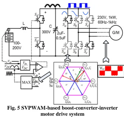
The circuit schematic and control system for a 1-kW boost converter inverter motor drive system is shown in Fig. 5. A 6ω dc-link voltage is generated from a constant
dc voltage by a boost converter, using open-loop control. Inverter then could be modulated by a SVPWAM method. The specifications for the system are input voltage is 100–200 V; the average dc-link voltage is 300 V; output line-to-line voltage rms is 230 V; and frequency is from 60 Hz to 1 kHz.
Fig. 5 SVPWAM-based boost-converter-inverter motor drive system
B. Voltage Constraint and Operation Region
It is worth noting that the SVPWAM technique can only be applied when the batteries voltage falls into the region Vin≤√3/2Vl−l due to the step-up nature of boost converter. The constraint is determined by the minimum point of the 6ω dc-link voltage. Beyond this region, conventional SPWM can be implemented. However, the dc-link voltage in this case still varies with 6ω because of the small film capacitor we selected. Thus, a modified SPWM with varying dc-link voltage will be adopted during the motor start up as shown in Fig. 16. Hence, the system will achieve optimum efficiency when the motor is operating a little below or around nominal voltage. When the motor demands a low voltage during start up, efficiency is the same as the conventional SPWM-controlled inverter.
Fig. 6 Operation region of boost-converter-inverter EV traction drive
In SVPWAM control of boost mode, dc-link voltage varies with the output voltage, in which the modulation index is always kept maximum. So, when dc-link voltage is above the battery voltage, dc-link voltage level varies with the output voltage. The voltage utilization increased and the total power stress on the devices has been reduced.
5. SIMULATION RESULTS
Fig. 7 Simulation Circuit of Existed System (2_Level SVPWAM)
Fig. 8 Output Voltages of Inverter
Fig. 9 THD Spectrum of Voltages
Fig. 10 Simulation Circuit of Proposed System (5-Level SVPWAM)
Fig. 11 Third Harmonic Waveforms for Injection
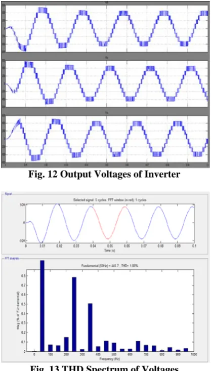
Fig. 12 Output Voltages of Inverter
Fig. 13 THD Spectrum of Voltages
6. CONCLUSION
In this paper, we have explained about both SVPWAM and SVPWAM. A 2-level SVPWAM and 5-level SVPWAM control techniques are developed for operating the inverters. It is observed that the proposed 5-level SVPWAM technique is having better performance. The THD of inverter output voltages is 3.26% and 1.06% in conventional and proposed systems respectively. The
effectiveness of the proposed method in reduction of power losses has been validated by the simulation results. REFERENCES
[1] D. M. Divan and G. Skibinski, “Zero-switching-loss inverters for high power applications,” IEEE Trans. Ind. Appl., vol. 25, no. 4, pp. 634–643, Jul./Aug. 1989.
[2] W. McMurray, “Resonant snubbers with auxiliary switches,” IEEE Trans. Ind. Appl., vol. 29, no. 2, pp. 355–362, Mar./Apr. 1993.
[3] J.-S. Lai, R. W. Young, Sr., G. W. Ott, Jr., J. W. Mc Keever, and F. Z. Peng, “A delta-configured auxiliary resonant snubber inverter,” IEEE Trans. Ind. Appl., vol. 32, no. 3, pp. 518–525, May/Jun. 1996.
[4] J. S. Kim and S. K. Sul, “New control scheme for ac-dc-ac converter without dc link electrolytic capacitor,” in Proc. 24th Annu. IEEE Power Electron. Spec. Conf., Jun. 1993, pp. 300–306.
[5] K. Rigbers, S. Thomas, U. Boke, and R. W. De Doncker, “Behavior and loss modeling of a three-phase resonant pole inverter operating with 120°A double flattop modulation,” in Proc. 41st IAS Annu. Meeting IEEE Ind. Appl. Conf., Oct. 8–12, 2006, vol. 4, pp. 1694–1701.
[6] J. Shen, K Rigbers, C. P. Dick, and R. W. De Doncker, “A dynamic boost converter input stage for a double 120◦ flattop modulation based three phase inverter,” in Proc. IEEE Ind. Appl. Soc. Annu. Meeting, Oct. 5–9, 2008, pp. 1–7.
[7] H. Fujita, “A three-phase voltage-source solar power conditioner using a single-phase PWM control method,” in Proc. IEEE Energy Convertes. Congr. Expo., 2009, pp. 3748–3754.
[8] H. Haga, K. Nishiya, S. Kondo, and K. Ohishi, “High power factor control of electrolytic capacitor less current-fed single-phase to three-phase power converter,” in Proc. Int. Power Electron. Conf., Jun. 21–24, 2010, pp. 443–448.
[9] X.Chen and M. Kazerani, “Space vector modulation control of an ac-dc-ac converter with a front-end diode rectifier and reduced dc-link capacitor,” IEEE Trans. Power Electron., vol. 21, no. 5, pp. 1470–1478, Sep. 2006.
[10] M. Hinkkanen and J. Luomi, “Induction motor drives equipped with diode rectifier and small dc-link capacitance,” IEEE Trans. Ind. Electron, vol. 55, no. 1, pp. 312–320, Jan. 2008.
[11] J. Jung, S. Lim, and K. Nam, “A feedback linearizing control scheme for a PWM converter-inverter having a very small dc-link capacitor,” IEEE Trans. Ind. Appl., vol. 35, no. 5, pp. 1124–1131, Sep./Oct. 1999.
[12] L. Malesani, L. Rossetto, P. Tenti, and P. Tomasin, “AC/DC/AC PWM converter with reduced energy storage in the dc link,” IEEE Trans. Ind. Appl., vol. 31, no. 2, pp. 287–292, Mar./Apr. 1995.
[13] T. Bruckner and D. G. Holmes, “Optimal pulse-width modulation for three-level inverters,” IEEE Trans. Power Electron., vol. 20, no. 1, pp. 82–89, Jan. 2005.
[14] F. Blaabjerg, S. Freysson, H.-H. Hansen, and S. Hansen, “A new optimized space-vector modulation strategy for a component-minimized voltage source inverter,” IEEE Trans. Power Electron., vol. 12, no. 4, pp. 704–714, Jul. 1997.
[15] M. M. Bech, F. Blaabjerg, and J. K. Pedersen, “Random modulation techniques with fixed switching frequency for three-phase power converters,” IEEE Trans. Power Electron., vol. 15, no. 4, pp. 753–761, Jul. 2000.
[16] F. Blaabjerg, D. O. Neacsu, and J. K. Pedersen, “Adaptive SVM to compensate dc-link voltage ripple for four-switch three-phase voltage-source inverters,” IEEE Trans. Power Electron., vol. 14, no. 4, pp. 743–752, Jul. 1999.
K. Jagdishwarji currently pursuing his M.Tech in Electrical Power System from J. B. Institute of
Engineering and Technology,
Affiliated to JNTU Hyderabad. He received his B.Tech degree from Vidya Jyothi Institute of Technology, Affiliated to JNTU Hyderabad, in 2013, and his field of interest includes Power Systems.
Email:
32TU[email protected]
U32TMONDI VINOD KUMAR received the B.Tech degree in Electrical & Electronics Engineering from VidyaJyothi Institute of Technology affiliated to JNTU Hyderabad in 2004, the M.TECH degree in Electrilcal Power systems from J. B. Institute of Engineering and Technology , Affiliated to JNTU Hyderabad, in 2008 , he was currently working as Assistant Professor at J. B. Institute of Engineering and Technology , Affiliated to JNTU Hyderabad, India. His area of interest include power system.
Email:
U[email protected]
Dr.S.Siva Prasad received Ph.D(Electrical) from JNTUH, Hyderabad. He received M.Tech degree from JNTU, Hyderabad and B.Tech from SV University. He0T0TCurrently working0T0Tas a
Professor and0T0THOD0T0Tin JB
Institute of Engineering0T0Tand
Technology (UGC Autonomous), Hyderabad, India. He received “Bharat Vibhushan Samman Puraskar” from “The Economic0T0Tand Human Resource Development
Association” in 2013 and received Young Investigator Award in 2012. His research0T0Tareas include Power
Electronics, Power Electronics &Drives, Facts Controllers.
Email:0T0T32TU[email protected]U32T