A Novel Compact Size Wilkinson Power Divider with Two
Transmission Zeros for Enhanced Harmonics Suppression
Eslam N. Mohamed*, Ayman G. Sobih, and Ayman M. El-Tager
Abstract—This paper presents a novel compact Wilkinson Power Divider (WPD) that improves harmonics suppression. The proposed WPD consists of a shunt open stub between two series similar inductors, and a microstrip line between an isolation resistor and each output port. This configuration acts as a low-pass filter with two transmission zeros. In addition, it facilitates manufacturability by using lower transmission line impedance values than conventional structures. Through even and odd mode analysis, the general design equations have been derived in closed form. A 2 GHz microstrip WPD is designed, fabricated and measured based on the proposed technique. A great agreement has been obtained between the measured performance of fabricated WPD circuit and the simulation results. The measured results show that the second and third harmonic levels are about −46 dB and −36 dB, respectively. The proposed design has about 40% reduction in size better than conventional WPD. It achieves competing results compared to other published work.
1. INTRODUCTION
Power dividers/combiners are very important parts representing fundamental components for microwave systems that facilitate the input for composing feeding networks for an array of antennas and high power amplifier sections. The major advantage of a conventional WPD is its good isolation between output ports and good matching at all ports. However, its major drawback is the presence of spurious responses due to quarter-wavelength transmission lines that increase the overall system nonlinearity [1]. Power dividers opportune solutions, present in literature, have been conceived to reach particular requirements such as low passive intermodulation distortion (PIM), compact size, wide bandwidth, and multi-band operations.
Recently, many researches are focused on minimizing the size and improving the harmonics suppression of power dividers using different techniques. Electromagnetic Band Gap (EBG) cells that exhibit band-stop and slow-wave characteristics are used in [2], but this technique faces some difficulties in modelling and fabrication since it relies on high resolution.
The technique of Defected Ground Structure (DGS), in [3, 4], depends on band stop characteristics, and it is easier than electromagnetic band gap in fabrication and equivalent circuit modelling, but its structure dimensions need design formulae, and their proper values are obtained iteratively. In addition, it needs backside etching. In [5], Defected Microstrip Structure (DMS) is used to prevent the leakage current through ground plane such as DGS, but it needs high resolution in fabrication. Planar artificial transmission line is presented in [6], High-low impedance resonator cells in [7], and Slow-wave structure in [8] which depends on reducing the group velocity of the propagated waves. All of the above techniques are based on intensive 3D EM simulations, while this paper adopts circuit analysis techniques having an advantage of providing helpful design equations and more precise results with reduced computational efforts.
Received 26 November 2017, Accepted 26 February 2018, Scheduled 13 March 2018
* Corresponding author: Eslam N. Mohamed ([email protected]).
On the other hand, some circuit-based designs utilizing stepped impedance transmission lines are introduced in [9, 10], but they depend on circuit optimization process and on shifting the spurious passband to other higher frequencies. In addition, other circuit-based designs rely on extra stubs and transmission lines as in [11, 12]. Since these designs depend only on microstrip lines, the post fabrication tuning is not possible to overcome the deviation between measured and required response if any. Therefore, lumped elements are presented, which play extra important roles in miniaturization and harmonic suppression such as capacitive loaded [13] and inductive loaded-based designs [14, 15].
In this paper, the inductor loaded design is adopted with the addition of two transmission zeros to improve the harmonic suppression performance by utilizing extra stub and a transmission line. Through even and odd mode analysis, the general design equations have been derived in closed form with the advantage of choosing the harmonic order which are required to be suppressed to suppressed [13] as in Section 2. Based on the derived equations, a design flows as well as design curves are proposed to facilitate the calculation-to-fabrication procedure, in Section 3. A 2 GHz microstrip WPD is designed, fabricated and measured to verify the proposed technique and show its advantages over other recent work as in Sections 4 and 5.
2. EVEN- AND ODD-MODE ANALYSIS
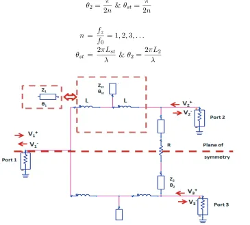
The quarter wave length 70.7 Ω microstrip line in the conventional WPD is replaced by two inductors (L) and a shunt open stub (Zst, θst) in the proposed design. Furthermore, the 100-Ω isolation resistor is replaced by a microstrip line (Z2,θ2) and lumped resistor (R) as shown in Fig. 1. Thus, the proposed
open stub and the transmission line can be utilized to add two transmission zeros in order to suppress the higher harmonics. Therefore, the electrical lengths (θstandθ2) of both elements can be determined
by means of the chosen frequency to be suppressedfz as follows:
θ2=
π
2n &θst= π
2n (1)
where
n = fz f0
= 1,2,3, . . . (2)
θst = 2πLst
λ &θ2 =
2πL2
λ (3)
whereLstand L2 are the physical lengths of open stub and microstrip lineZ2, respectively.
Firstly, for simplicity, one assumes that the two series inductors and shunt open stub are equivalent to transmission lineZ1 andθ1 in two square dashed as shown in Fig. 1. The modeling starts with even
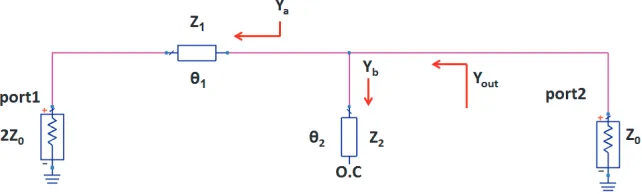
analysis as shown in Fig. 2 to obtainZ1 and θ1.
Figure 2. Equivalent circuit for even mode analysis of the proposed design.
The output ports matched to characteristic impedance admittance Yout equaly0;
Yout = Ya+Yb (4)
Ya = y0y1+jy
2 1tanθ1
2y1+jy0tanθ1
(5)
Yb = jy2tanθ2 (6)
where
θ1 =
2πL1
λ (7)
Yout = y0 =
y0y1+jy21tanθ1
2y1+jy0tanθ1
+jy2tanθ2 (8)
Equating real and imaginary parts in Equation (8) deduces that:
−Z2
Z1
= tanθ2tanθ1 (9)
1−y0Z
2 1
2 =
y2 0
tan2θ 1
(10)
Substituting Equation (9) in Equation (10) obtains:
Z1 = Z0Z¯2
2 ¯ Z2
2 + 2 tan2θ2
(11)
θ1 = π−tan−1
Z
2
Z1tanθ2
(12)
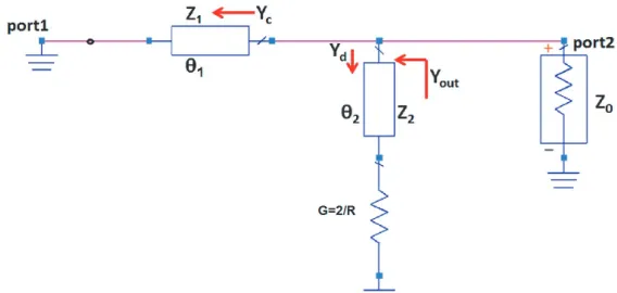
In odd-mode analysis, the equivalent circuit can be redrawn as shown in Fig. 3 to obtain isolation resistorR and microstrip line impedanceZ2 which is responsible for the second transmission zero. The
total output admittance must equal y0, and it can be expressed as:
Yout =Yc+Yd (13)
where:
Yc = −jy1cotθ1 (14)
Yd = Gy2+jy
2 2tanθ2
y2+jGtanθ2
(15)
Yout = y0 =
Gy2+jy22tanθ2
y2+jGtanθ2 −
Figure 3. Equivalent circuit for odd mode analysis.
By equating the real and imaginary parts of Equation (16) we get
G= y0
1−tan2θ 2
(17)
From Equations (16) and (17) R and Z2 can be calculated as:
R = 2Z0
1−tan2θ2
(18)
Z2 = Z0
2 (1−tan2θ2) (19)
Equations (18) and (19) indicate that the lumped resistance and impedance value of the extra-transmission line depend only on its electrical length.
Finally,ABCDmatrix is used to equate the inductor and stub T network with its equivalent circuit Z1 andθ1 of Fig. 1, obtaining design equation for the inductor and stub impedance.
TheABCD matrix of series inductor “L”:
M1 =
1 −jωL
0 1
(20)
The ABCDmatrix of the microstrip line z1 is:
Mtotal=
cosθ1 jz1sinθ1
jy1sinθ1 cosθ1
(21)
The ABCDmatrix of shunt stubzst is:
Mst =
1 0
jysttanθst 1
(22)
Mtotal = M1MstM1=
1 +ωLysttanθst −2jωL−jω2L2ysttanθst jysttanθst 1 +ωLysttanθst
(23)
By equating elements of the two matrices in Equations (21) and (23) we deduce that:
cosθ1 = 1 +ωLysttanθst (24)
z1sinθ1 = −2ωL−ω2L2ysttanθst (25)
y1sinθ1 = ysttanθst (26)
From Equations (24) and (26), we get:
zst = z1tanθst sinθ1
(27)
ωL = zst|cosθ1−1|
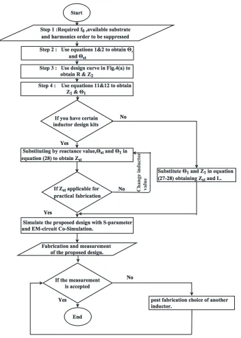
Therefore, the inductor as well as the stub line can be designed based on Equations (27) and (28). The next section describes the utilization of these equations in a proposed design algorithm. These are the closed form equations used to achieve the proposed design based on direct calculations rather than circuit optimization or 3D EM simulation.
3. PROPOSED DESIGN FLOW
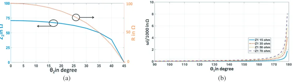
Based on the derived equations in the previous section, Fig. 5 helps designers to calculate circuit parameters. The design curves of Fig. 4(a) can be used to determine the impedance of Z2 and isolation
resistor R depending on the chosen electrical length θ2. The available lumped inductors are always
restricted to certain values in the standard kits. Thus, the design curve of Fig. 4(b) can be used to choose appropriate reactance value based on certain inductor kit to obtain impedance Z1 and its
electrical length θ1.
(a) (b)
Figure 4. Design curves (a) Z2 and isolation resistor versusθ2, (b) reactance versus θ1.
Starting from the circuit specification such as fundamental frequency, harmonics order required to be suppressed and available substrate parameters, the design flowchart illustrated in Fig. 5 gives the designer main guidelines to reach a complete design achieving certain desired response. The flowchart gives the designer some degree of freedom to choose different circuit parameters suitable for manufacturing facilities and inductors values in the available standard kits. A small code could be written easily based on this proposed algorithm for automating the circuit design by some initial guess for the inductor values from the available design kits. The termination from this loop is obtained by the easily fabricated stubs based on the available substrates.
4. A 2 GHZ MODIFIED WPD BASED ON THE PROPOSED DESIGN
4.1. Initial Design and Calculations
To demonstrate the proposed design technique, a WPD has been designed at centre frequency of 2 GHz by applying the algorithm discussed above. The shunt open stub and the extra-transmission line are dedicated for the 2nd and 3rd harmonics suppression, respectively. The designed circuit has been
Table 1. Calculated design parameters using the proposed technique.
Parameter Impedance
(Ω)
Electrical length (deg.)
Physical width (mm)
Physical length (mm)
Z2 57.7 30 1.8 9.1
Zst 52.3 45 2.1 13.7
Z0 50 10 2.3 3
Figure 5. Flow chart of the proposed design methodology.
fabricated on a Rogers’ RT/Duroid 5880 substrate with a dielectric constant of 2.2, thickness of 0.787 mm and loss tangent of 0.0009.
Using Equations (1) and (2), the electrical lengths are calculated (θ2 = 30◦, θst = 45◦). From Fig. 4(a), R and Z2 can be obtained as 66.7 Ω and 57.7 Ω, respectively. The details of obtained circuit
parameters are illustrated in Table 1, while the used lumped inductor (L = 5.6 nH) is selected from one of the available standard design kits such as EPCOS (TDK). Zstcan be determined from Eq. (28) as 52.3 Ω. Zst and Z2 are found to be applicable as shown in Table 1. It is worth to note that some
4.2. Circuit Simulation
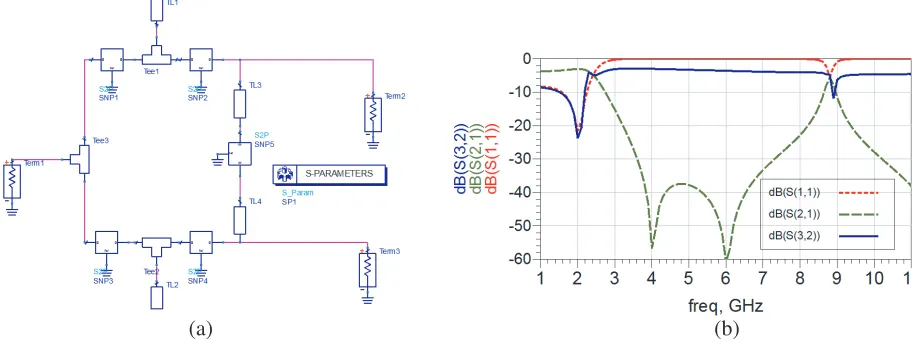
In order to verify the proposed design technique, the Advanced Design System (ADS) from Keysight Tech. is used. An S-parameter simulation has been applied to the schematic circuit of the modified WPD developed in Fig. 6(a), based on the calculated parameters of Table 1. The simulation results are shown in Fig. 6(b) where it can be noticed that the designed circuit satisfies all of the desired specifications with excellent suppression for the 2nd harmonic (at 4 GHz) and 3rd harmonic (at 6 GHz) with 52 dB and 58 dB, respectively.
(a) (b)
Figure 6. (a) Schematic circuit of the designed WPD, (b)S-parameters simulation results.
Indeed, lumped and distributed components suffer from manufacturing tolerances. Therefore, it is necessary to study manufacturing tolerances affecting the circuit performance. Monte Carlo simulation is applied with±5% tolerance in inductor and resistor values, and about±5% photolithographic tolerance in length and width of microstrip lines. Monte Carlo yield analyses are obtained by adjusting certain yield specification for S-parameter within bandwidth from 1.9 GHz to 2.1 GHz. Variation of S21 is
adjusted from −3 to −3.5 dB, S32 better than −10 dB, and S11 better than −10 dB. Moreover, the
second and third harmonics can be accepted lower than−30 dB with 100 MHz bandwidth. The number of samples to be simulated is 2000. Numbers of passed and failed samples are as shown in Fig. 7. The passed samples represent 95.05% which can achieveS-parameters and Harmonic Isolation specifications within the acceptable range as specified above. This verifies that the proposed design is insensitive to fabrication and component tolerances.
Figure 7. Yield simulation results showing numbers of pass and fail samples.
4.3. Layout and EM-Circuit Co-Simulation
The layout of the designed circuit has been generated by the ADS software package, and an EM circuit Simulation has been applied to the generated layout as shown in Fig. 8(a). The EM circuit Co-Simulation results are shown in Fig. 8(b) from which it can be seen that an accurate power division is achieved over the frequency band of interest (up to 2.2 GHz),S21=S31=−3.1 dB. In addition, a very
(a) (b)
Figure 8. (a) Layout of the designed WPD, (b) EM circuit co-simulation results.
Therefore, the proposed modified WPD is not that sensitive to microstrip discontinuities as well as coupling between close lines.
5. FABRICATION AND MEASUREMENTS
The designed and simulated circuit of the modified WPD has been fabricated on a specified substrate using photolithography technique, and a photograph of the fabricated circuit is illustrated in Fig. 9. The overall dimensions of the circuit are 5.1 mm (0.051λg) in width and (33.048) mm (0.326λg) in length with total area about 168.5 mm2, which has 40% reduction compared to that of a conventional WPD. The measured S-parameters of the fabricated circuit compared to the EM co-simulation results are shown in Fig. 9. From the figure it can be noticed that a good agreement is obtained between them, and the fabricated circuit satisfies the desired specifications. The fabricated power divider has return loss better than 10 dB from 1.83 GHz to 2.21 GHz, insertion loss about 0.5 dB and output ports isolation better
(a) (b)
(c) (d)
Figure 9. Measured versus simulated (a) S11, (b) S21, (c) S32 and (d) photograph of the fabricated
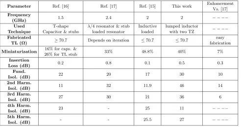
than 25 dB in band. The measured isolation is a bit shifted from the simulated one, but fortunately it is wider in band and better in value. Therefore, this small shift does not affect the isolation performance. In addition, the maximum achievable harmonic suppressions are 46 dB and 36 dB for the 2nd and 3rd harmonics, respectively, assuming 0 bandwidth. They are still better than what is reported in [17] by at least 3 dB for both 2nd and 3rd harmonics with bandwidths of 143 MHz and 100 MHz, respectively. A comparison between the proposed modified design of the WPD and other similar recently published work is given in Table 2. Up to the authors’ knowledge, this proposed divider achieves enhanced performance better than the best reported one [17] by 7% in miniaturization, at least 6 dB in harmonics isolation and 0.3 dB in insertion loss while providing easy fabrication and closed form design equations with clear algorithm. These promising results prove that the proposed design equations are fairly accurate and help the designer to avoid going through intensive circuit optimization or 3D EM simulation, while offering design degree of freedom regarding the inductor choice.
Table 2. Comparison between the proposed modified WPD and recent publications.
Parameter Ref. [16] Ref. [17] Ref. [15] This work Enhancement
Vs. [17]
Frequency
(GHz) 1.5 2.4 2 2 − − −−
Used Technique
T-shape Capacitor & stubs
λ/4 resonator & stub loaded resonator
Inductive loaded
lumped inductor
with two TZ − − −−
Fabricated
TL (Ω) ≥70.7 Depends on iteration ≤70.7 ≤70.7
easy fabrication
Miniaturization 16% for caps. &
26% for TL stub 33% 48.8% 40% 7%
Insertion
Loss (dB) 0.2 0.8 0.1 0.5 0.3
Fund.
Isol. (dB) 22 20 17 30 10
2nd Harm.
Isol. (dB) 11 32 11.9 46 14
3rd Harm.
Isol. (dB) 27 30 21 36 6
4th Harm.
Isol. (dB) 23 - 25 11 − − −−
5th Harm.
Isol. (dB) - - 25.5 27 − − −−
6. CONCLUSION
In this paper, a modified compact WPD with two transmission zeros for improved harmonics suppression has been presented. The proposed design consists of shunt open stub between two series inductors and an extra microstrip line with isolation resistors at output ports. The lumped inductors provide better harmonic suppression, size reduction, and design degree of freedom. The general design equations for the proposed WPD are derived in closed form, while a flowchart for the design procedure has been presented as well. The proposed design equations and methodology are verified through fabrication and measurements of a 2 GHz modified WPD circuit. It achieves 46 dB and 36 dB suppressions for the 2nd and 3rd harmonics, respectively, while satisfying the other required specifications. Very good agreement has been obtained between the measured performance of the fabricated WPD and the EM circuit co-simulation results. This verifies the proposed technique as well as the design methodology.
equations with clear algorithm. These promising results prove that the proposed design equations are fairly accurate and help the designer to avoid going through intensive circuit optimization or 3D EM simulation, while offering design degree of freedom regarding the inductor choice.
REFERENCES
1. Li, J., Y. Liu, S. Li, C. Yu, and Y. Wu, “A novel multi-way power divider design with enhanced spurious suppression,” Applied Computational Electromagnetics Society Journal, Vol. 29, No. 9, Sep. 2014.
2. Lin, C.-M., et al., “Wilkinson power divider using microstrip EBG cells for the suppression of harmonics,” IEEE Microwave and Wireless Components Letters, Vol. 17, No. 10, 700–702, Oct. 2007.
3. Liu, H., et al., “Harmonic-rejection compact band pass filter using defected ground structure for GPS application,” Active and Passive Electronic Components, Apr. 2014.
4. Yu, W.-H., et al., “A compact filter with sharp-transition and wideband-rejection using the novel defected ground structure,”Journal of Electromagnetic Waves and Applications, Vol. 23, Nos. 2–3, 329–340, Jan. 2009.
5. Xiao, J.-K. and W.-J. Zhu, “New defected microstrip structure band stop filter,” PIERS Proceedings, 1471–1474, Suzhou, China, Sep. 12–16, 2011.
6. Yang, T., C.-J. Liu, L. Yan, and K.-M. Huang, “A compact dual-band power divider using planar artificial transmission lines for GSM/DCS applications,” Progress In Electromagnetics Research Letters, Vol. 10, 185–191, 2009.
7. Hayati, M., A. Abdipour, and A. Abdipour, “A Wilkinson power divider with harmonic suppression and size reduction using high-low impedance resonator cells,” Radio Engineering, Vol. 24, No. 1, 137–141, Apr. 2015.
8. He, J., B.-Z. Wang, and W. Shao, “Compact microstrip power dividers with slow wave structure and capacitor loading,”IEEE International Conference on Microwave and Millimeter Wave Technology
(ICMMT), 52–55, May 2010.
9. Sedighy, S. H. and M. Khalaj-Amirhosseini, “Compact Wilkinson power divider using stepped impedance transmission lines,”Journal of Electromagnetic Waves and Applications, Vol. 25, No. 13, 1773–1782, Jan. 2011.
10. Deng, P.-H., J.-H. Guo, and W.-C. Kuo, “New Wilkinson power dividers based on compact stepped-impedance transmission lines and shunt open stubs,” Progress In Electromagnetics Research, Vol. 123, 407–426, 2012.
11. Ip, W.-C. and K.-K. M. Cheng, “A novel unequal power divider design with dual-harmonic rejection and simple structure,”IEEE Microwave and Wireless Components Letters, Vol. 21, No. 4, 182–184, Apr. 2011.
12. Yang, N., B. Li, and X. Wu, “Closed-form design of Wilkinson power divider with broadband harmonic suppression and size reduction,” Journal of Electromagnetic Waves and Applications, Vol. 26, Nos. 2–3, 307–318, Jan. 2012.
13. Ning, J., et al., “A new design of compact microstrip Wilkinson power dividers,” 2014
IEEE International Symposium on Radio-Frequency Integration Technology (RFIT), 1–3, IEEE,
Aug. 2014.
14. Fan, F., Z.-H. Yan, and J.-B. Jiang, “Design of a novel compact power divider with harmonic suppression,”Progress In Electromagnetics Research Letters, Vol. 5, 151–157, 2008.
15. Mohamed, E. N., A. G. Sobih, and A. M. El-Tager, “Compact Wilkinson power divider with inductive loaded microstrip line for harmonics suppression,” 2016 IEEE Middle East Conference
on Antennas and Propagation (MECAP), 1–4, IEEE, Sep. 2016.
16. Li, J.-L., et al., “Miniaturized Wilkinson power dividers with harmonic suppressions,”
Electromagnetics, Vol. 36, No. 3, 157–166, Apr. 2016.