Design of Compact Double-Layer Microwave Absorber for X-Ku
Bands Using Genetic Algorithm
Hesham A. El-Hakim1, *, K. R. Mahmoud2, and A. A. Abdelaziz1
Abstract—In this paper, an efficient lightweight double-layer microwave absorber with
impedance-matching structure at X-Ku bands was designed, optimized and implemented. First, genetic algorithm (GA) was considered to optimize the thicknesses and material properties for better absorption of the incident electromagnetic wave and reduction of radar cross section (RCS). Next, with the aid of the obtained dielectric and magnetic properties, the microwave absorber was fabricated from magneto-dielectric composite materials besides a natural rubber. Finally, the analytical and numerical results were compared with the measurements to check the validity of the design. Experiments showed that the reflection coefficient for each layer backed with a metallic sheet was insufficient; however, for the
double layer absorber, the reflectivity measurement values reached up to −28 dB in the case of normal
incidence and −17 dB for oblique incidence.
1. INTRODUCTION
Recently multilayer broadband with both magneto-dielectric composite materials is used as one of the cloaking techniques for either planar layered structure or rounded shape objects based on transforming the electromagnetic energy into heat [1, 2]. Multilayer broadband absorbers have been considered in many engineering applications, especially, for the design of microwave shielding enclosures, anechoic chambers to ensure electromagnetic compatibility (EMC), wireless telecommunication systems and
stealth technology as radar-absorbent material (RAM) [3]. Designing of absorbing materials with
desirable attenuation is of great importance over selective or wideband frequency either by bulky, sheet or shaped around different objects material [4, 5]. The materials of interest should provide the required reflectivity attenuation of near-field or far-field electromagnetic waves for different objects at varieties of incident angles and polarizations. Absorber materials must have light weight, low cost, good thermal, mechanical and chemical properties and should pass a physomechanics and environmental testes for thick or thin layers [5–7].
In [8], a four-layer radar absorbing coating for RCS reduction at X-band was implemented using
genetic algorithm (GA). It was found that the minimum RCS of 55.66 m2 was obtained after 4 layers of
coating with thickness of 5.015 mm at 8 GHz. A reflectivity value less than−13 dB was achieved by using
double-layer absorber by mixing a rubber with magnetic micropowder and/or dielectric materials [5]. The design of double-layer absorber based on nanocomposite materials to achieve simplicity in mixing material particles with the host medium and obtain uniform dispersion is discussed in [9–11]. In [9], a four-layer absorber with total thickness of 7 mm was designed using GA and tested in X-band for
5◦ incident angle, achieving a reflectivity value greater than −10 dB. In [10], a double-layer absorber
with total thickness of 2 mm was made from magnetic nanocrystalline alloy Fe0.2 (Co0.2Ni0.8)0.8 and
nanocomposite SrFe12O19/Ni0.5Zn0.5Fe2O4 microfibers, and the obtained reflectivities were found to be
Received 17 November 2015, Accepted 13 January 2016, Scheduled 25 January 2016 * Corresponding author: Hesham Abd El-Hakim ([email protected]).
less than−10 dB for the desired bandwidth from 10.7 to 18 GHz except at 12.1 GHz that had a reflection
loss of−71.4 dB. A double-layer absorber based on nanocomposite BaFe12O19/α-Fe and nanocrystalline
α-Fe micro fibers was considered in [11], with a total thickness of 3.5 mm. For a bandwidth ranging from
5.3 to 18 GHz, the obtained reflectivity values were greater than−20 dB in the case of normal incident
angle. In [12], a reflection loss of −29.56 dB was achieved at 11.7 GHz for doped barium hexaferrite
based absorber structure with a total thickness of 2 mm. A reflection loss value of−24.3 dB was achieved
at 12.02 GHz for a double-layer CoZn-ferrite/TiO2 microwave structure in [13].
In this paper, a compact double-layer microwave absorber is designed and implemented in which the thickness of both layers as well as their material properties have been optimized with the aid of GA such that the backscatter RCS is minimized. The paper focuses on the TE (transverse electric) polarization, which implies that the electric field is transverse to the incidence plane. The first layer is a rubber ferrite composites made up of ferrimagnetic powders and rubber as a host material used for confining incident wave through the overall structure, while the second layer comprises a rubber compounds loaded with a conductive powders to have better specular reflection attenuation properties over a wide frequency range (8–18 GHz). The reflection of the incident wave is reduced based on the impedance matching principle of the first layer with a free space, while the second layer provides good microwave power absorption placed on the surfaces to be protected from unwanted radiation [14]. The arrangement for both dielectric and magnetic particles in a structure ended with metallic sheet is designed to provide best impedance matching for the incident wave and better electric, magnetic loss with smaller thickness for both layers [5]. Specular wideband analysis has been considered to study the material properties for each layer to cover the frequency band. The measurements are compared to the analytical and numerical results to check the validity of the design.
The paper is divided as follows. Section 2 describes the problem formulation. In Section 3, a brief description to material properties optimization is introduced. Section 4 presents the fabrication and samples measurements. Finally, Section 5 presents the conclusion.
2. PROBLEM FORMULATION
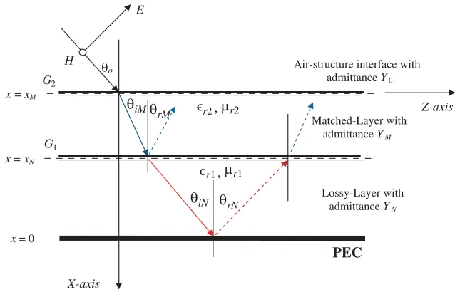
The design of radar absorbing materials (RAM) consists of a sequence of multilayers in front of a PEC plane require an implementation of electromagnetic (EM) model in which the knowing of the reflection coefficient at the first (air-multilayer) interface is of a great importance. Both normal and oblique incident waves can be applied, and the amplitudes of forward and backward propagated waves are calculated at the interface between any layers, beginning from the adjacent layer to a metallic sheet until the air-matched layer interface.
X-axis
PEC
θo
E
H G2
Air-structure interface with admittance Y0
μr2
Lossy-Layer with admittance YN
Z-axis
Matched-Layer with admittance YM
x = 0
x = xN
x = xM
r2
θiMθrM
μr1
r1
G1
θiN θrN ∋
∋ ,
,
Assuming the EM model of a double-layer absorber structure for transverse electric (TE) mode
with infinitesimally thin resistive sheets (ideally, zero thickness) of conductance G1 and G2 as shown
in Fig. 1. The electric field intensity E and magnetic field intensity H for any arbitrary layer x are as
follows [15]:
E = Pie−jk(−xcosθ+zsinθ)+Prejk(xcosθ+zsinθ) (1)
H = Y
Pie−jk(−xcosθ+zsinθ)+Prejk(xcosθ+zsinθ)
(2)
The boundary conditions on the tangentialE and H fields to be satisfied at theG1 interface are:
G1E+=G1E−=J, H+−H−=J, kMsinθM =kNsinθN (3)
where the plus and minus subscripts denote the fields on opposite sides of the lossy-matched layer
interface, and J is the current density in the sheet.
By applying Equation (3) in Equations (1) & (2), we get:
PiMe−jkM(xNcosθiM+zsinθiM)+PrMejkM(xNcosθrM+zsinθrM)
= PiNe−jkN(xNcosθiN+zsinθiN)+P
rNejkN(xNcosθrN+zsinθrN) (4)
And
YM
PiMe−jkM(xNcosθiM+zsinθiM)−PrMejkM(xNcosθrM+zsinθrM)
= (G1+YN)PiNe−jkN(xNcosθiN+zsinθiN)+ (G1−YN)PrNejkN(xNcosθrN+zsinθrN) (5)
The amplitudes of the incident and reflected propagated waves, Pi and Pr respectively at the
air-structure interface, are then calculated by applying an iterative procedure to implement Maxwell’s
equations starting from the PEC plane at x = 0 where Pi = 1 and Pr = −1, until the
air-matched interface passing through N and M layers as in Equations (4)–(5) with linear boundaries
transformation [15].
Pi = e
jk0xMcosθ0
2Y0cosθ0
P
iM(Y0cosθ0+YMcosθiM+G2)e−jkMxMcosθiM
+PrM(Y0cosθ0−YMcosθrM+G2)ejkMxMcosθrM
(6)
Pr = e
−jk0xMcosθ0
2Y0cosθ0
PiM(Y0cosθ0−YMcosθiM−G2)e−jkMxMcosθiM
+PrM(Y0cosθ0+YMcosθrM−G2)ejkMxMcosθrM
(7)
where, xN is the distance from the surface of PEC to the interface between lossy layerN and matched
layer M;xM is the distances from surface of PEC to the air-matched interface; k0 =ω0√ε0μ0, kM =
k0√μrMεrM and kN = k0√μrNεrN are the wave number of the free-space, layer M, and layer N,
respectively; G is the conductance moh/sq of thin resistive sheet at the interface between layers;
Y0 = 1/377 Ω−1,YM =
εM/μM are the free space and Mth layer intrinsic admittance normalized to
Y0 respectively.
The reflection coefficient, Γ, of the air-structure interface can be calculated by:
|Γ|=−20log10
Pr
Pi
(8)
The transmission coefficient T =e−γx where γ = γ0√με is the complex propagation constant in the
material and γ0 =j2π/λ0 the free space propagation constant. The reflection loss (S11) and insertion
loss (S21) parameters are related to the parameters Γ and T by the following equations [16]:
S11 =
Γ(1−T2)
1−Γ2T2 (9)
S21 = T
(1−Γ2T2)
1−Γ2T2 (10)
The material complex permittivity and permeability constants can be calculated by:
r = r−j r = γγ
0
1−Γ
1 + Γ (11)
μr = μr−jμr = γγ
0
1 + Γ
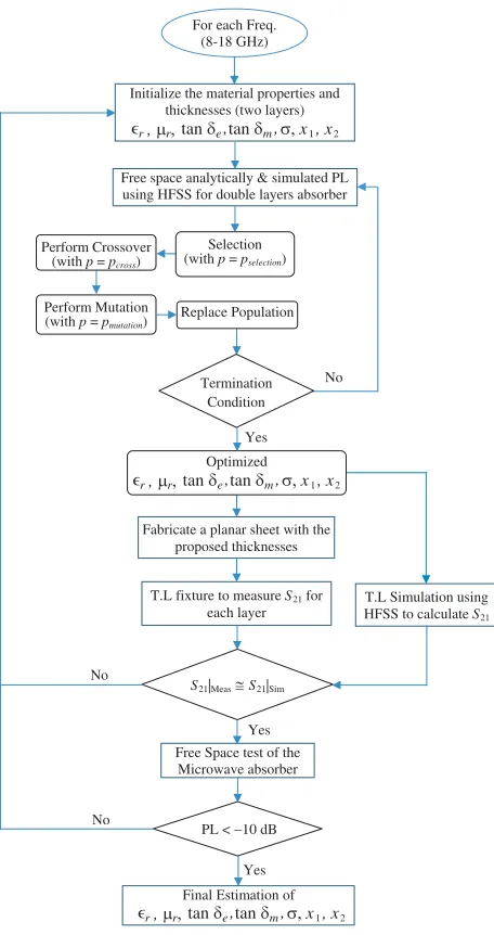
In the current work, the design of compact double-layer microwave absorber with absorption
performance level greater than −10 dB absorption has been considered according to the methodology
flow chart depicted in Fig. 2. The methodology is started by initializing material properties for both layers (complex permittivity, complex permeability, conductivity, electrical and magnetic loss tangent)
and thicknesses. The preliminary return power loss values (PL) at air-structure interface can be
calculated analytically by implementing a computer Matlab code for Equations (1) through (8) and numerically by using a computer aided computation method Ansoft HFSS. The optimization technique is then applied both analytically to establish the previous estimated values and with consistence of numerical model using HFSS to get the optimized material properties for each absorber structure. The presented GA optimization tool had a goal of obtaining a thin compact-layer structure with the best selection of material properties and thickness of each layer in which the loss of electromagnetic energy inside the engineered structure fulfilled more than 90% losses, which means a reflection coefficient value
lower than −10 dB at the air-sample interface [9]. With the aid of previous analytical and numerical
Free space analytically & simulated PL using HFSS for double layers absorber
S21|Meas S21|Sim
Fabricate a planar sheet with the proposed thicknesses
T.L fixture to measure S21 for
each layer
Free Space test of the Microwave absorber
PL < −10 dB
Final Estimation of
T.L Simulation using
HFSS to calculate S21
Initialize the material properties and thicknesses (two layers)
r μ ,r
For each Freq. (8-18 GHz)
Selection
(withp=pselection)
Perform Crossover
(withp=pcross)
Perform Mutation
(withp=pmutation) Replace Population
Termination Condition
No
Yes
Yes No
Optimized
No
Yes ∋ tan δ
etan δm σ, x , x
, , , 1 2
r∋ ,μ ,r tan δe,tan δm,σ, x , x1 2
≅
r μ ,r
∋ tan δ
etan δm σ, x , x
, , , 1 2
Figure 2. Methodology flow chart diagram.
(a)Matched layer
(b)Lossy layer
Figure 3. The optimized relative dielectric and
modelling, the two composite material layers in the frequency band from 8 to 18 GHz are designed and manufactured using mixing rules to select proper combination of materials. The concentration for both host (matrix, base) material and inclusions with their configuration is studied to fulfil high absorption over a frequency range of interest. The natural rubber (host medium) was chosen as commercially low cost polymer host material for both layers. By adding suitable inclusions to the host medium according to the mixture law of materials, the fabricated planar sheets are then obtained with the optimized thicknesses. Also, a specular analysis of the given layers is considered through the transmission line
fixture T.L. within the entire bandwidth (8–18 GHz) to measure the insertion loss S21 for both layers.
Validation of the measurement with the theoretical analysis and numerical model is an important stage
of the methodology [17]. Therefore, theS21results for both measured and simulated T.L. are compared
for the purpose of extracting the best material properties for the two layers. If the measured and simulated insertion losses are comparable, the performance of the structure will be evaluated by free space measurements to determine the reflectivity of the structure for each layer separately, then for
the double-layers in front of a metallic sheet. An acceptable return power loss of −10 dB is defined as
a minimum threshold absorption level which must be fulfilled by the fabricated planar structure. If the desired absorption level was achieved, estimated values of the above material properties would be considered and used in the analytical and simulated free space PL calculations.
3. MATERIAL PROPERTIES OPTIMIZATION
A genetic algorithm (GA) has been applied for the purpose of optimizing the thickness of both layers besides their material properties selections, in which frequency-dependent material properties for various layers have been optimized to improve the RCS reduction for the proposed double-layer absorber over X-Ku bands. GA is a search iterative algorithm which mimics the process of natural evolution by performed solutions in evolutionary computation methods. GA is a very powerful optimization technique for problems that have a large number of variables. GAs operate on a population of potential solutions, starting with randomly selected populations within the decision space, then apply a repetitive iterations to that populations with the principle of survival of the fittest to produce better and better approximations to minimize the objective functions [18]. At each generation, a new set of approximations is created by the process of selecting individuals according to their level of fitness in the problem domain from the data base of the materials, breeding them together using natural genetics operators [19]. The brief pseudo-code of the GA algorithm has been provided below:
BEGIN
1. INITIALIZE population with random candidate solutions;
2. EVALUTE each candidate;
3. FOR EACH ITERATION
SELECT parents;
RECOMBINE pairs of parents;
MUTATE the resulting offspring;
EVALUATE new candidates;
SELECT individuals for the next generation;
4. REPEAT UNTIL (TERMINATION CONDITION is satisfied).
END
The main objective is to design a double-layer absorber for reducing the radar cross section of
overall structure in which RC = |Γ|, where, RC at the first air-multilayer interface Equation (8) has
been considered as the most important parameter for the GA objective function. Both oblique and
normal incidence cases have been considered through robust optimization. The following equation
illustrates the considered objective function:
Objfun= minfmax
fmin
θmax
θminRC
x1, r1, r1, μr1, μr1, σ1, x2, r2, r2, μr2, μr2
where,x1, x2are the thicknesses of the two layers. r1, r1, r2, r2are the real and imaginary permittivity
parts of both layers. μr1, μr1, μr2, μr2 are the real and imaginary permeability parts of both layers. σ1
is the lossy layer conductivity, where σ2 is set to zero for a good matched absorber, θmin = −90◦,
θmax = 90
◦
. Table 1 illustrates the decision space for each parameter to be optimized [8]. The GA optimization parameters are selected as shown in Table 2.
Figures 3(a) and 3(b) show the optimized relative permittivity and permeability constants for both matched and lossy layers, respectively, over the desired bandwidth. The design of the proposed RAM
Table 1. Parametersdecision space and the average optimized materials propertiesusing GA.
Variables Decision Space Average value
min value max value
r1 5.5 7 6.10889
r2 1.5 3.5 2.43639
μ
r1 0.7 2.5 1.7078
μ
r2 1 3 1.98
σ1 (Siemens) 0.12 0.3 0.2229
r1 0.11 0.63 0.40489
r2 10−4 5.5×10⁻⁴ 4.48×10⁻⁴
μ
r1 0.021 0.75 0.576
μ
r2 0.5 3 1.239
x1 (mm) 2.2 3.3 2.5
x2 (mm) 1.2 2.3 1.5
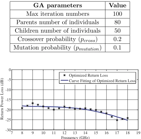
Table 2. The GA optimization parameters.
GA parameters Value
Max iteration numbers 100
Parents number of individuals 80
Children number of individuals 50
Crossover probability (pcross) 0.2
Mutation probability (pmutation) 0.1
7 8 9 10 11 12 13 14 15 16 17 18 19
-30 -25 -20 -15 -10 -5 0
Frequency (GHz)
Return Power Loss (dB)
Optimized Return Loss
Curve Fitting of Optimized Return Loss
Figure 4. Optimized return power loss of double layer absorber backed with PEC (oblique incident
structure with the aid of GA fulfilled an improvement in absorption level over a wide bandwidth as
shown in Fig. 4 with optimized layers thicknesses x1 = 2.5 mm, x2 = 1.5 mm. It has been shown that
the GA achieved a robust solution in choosing the appropriate material properties for both layers among the range spaces for different input variables with a decision space reported in Table 1.
4. SAMPLES FABRICATION AND MEASUREMENT
Since a composite material consists of more than one material phase and a host medium such as rubber which represents the dielectric base and inclusion materials which represent conducting, non-conducting medium or both, the usage of an analytical formulation such as mixing rule will be a good tool in designing the proposed compact double layer absorber and providing the effective medium permittivity and permeability as a function of composite concentration and desired frequency. There are many mathematical models to get the best mixing formulation suitable for treatment with either low or high concentration of conductive inclusions as well as treatment with ferrimagnetic powders [17]. The fabrication has been done in the desired frequency range according to the average values of optimized material parameters as reported in Table 1. With the aid of the measurements, modelling and analytical analysis, we obtained the final fabricated layer sheets. In the first layer, the natural rubber was loaded with a high permeability, magnetic loss stable and economical ferrimagnetic (ferrite) powders in addition to low density graphite powder (50% ferrimagnetic powders, 6.5% graphite and 1.5% carbon fibre) in
order to confine electromagnetic energy through the structure with resistive value close to 377 (Ω/m2)
providing low RF loss. Absorption was achieved in the second layer composed of rubber as a host medium loaded with a high structure of carbon powder (45%) allowing the medium to be highly conductive but was thicker than the matching one [20, 21].
4.1. The Microstrip Line Modelling and Measurement
Microstrip line device was used for broadband measurement of complex relative dielectric ( r) and
relative permeability (μr) constants of RAM at microwave frequencies. The device has a characteristic
impedance of 50 Ω to match coaxial cables and vector network analyser (VNA), r = 3.2, tanδe= 0.001
and cross section area (80 mm×40 mm ×1.6 mm). The absorber samples have cross section area
1.5 cm×1.5 cm and thickness 2.5 mm for the first layer, and 1.5 mm for the second one. A specular
analysis is performed to obtain the complex permeability (μr) and complex permittivity ( r) of each
RAM layer as a function of frequency by connecting the microstrip line through coaxial cables to both
ports of (VNA), and the sample under test is loaded directly on the line. Then, the S-parameters
are computed for both transmission and reflection (T/R method) in which the reflection loss S11 and
insertion lossS21 were given for each absorber layer through the desired bandwidth by using
computer-controlled network analyzer such as the Rohde & Schwarz Model ZVA 67 [22]. The power loss can be calculated using the following Equation (9):
P ower Loss% =1−S112 −S221·100 =
1− |Γ|2− |T|2
·100 (14)
An HFSS simulation model for the section of microstrip line device described above was also executed
where the calculation of S21 for each absorber layer became a crucial point for the selection study of
material properties parameters by verifying the obtained simulated with measurementS21 [9].
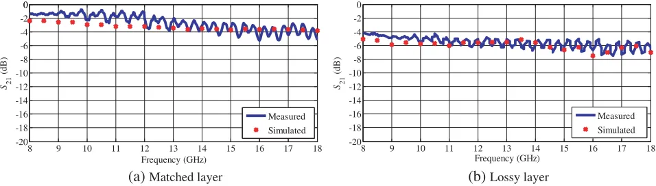
Figures 5(a) and 5(b) show the insertion loss comparison between the measured and simulated results using the transmission line technique of the designed matched and lossy layers, respectively.
With the aid of HFSS software package, the complex values of r and μr can be evaluated. As shown
(a) Matched layer (b) Lossy layer
8 9 10 11 12 13 14 15 16 17 18
-20 -18 -16 -14 -12 -10 -8 -6 -4 -2 0 0
Frequency (GHz)
S21
(d
B
)
Measured Simulated
8 9 10 11 12 13 14 15 16 17 18
-20 -18 -16 -14 -12 -10 -8 -6 -4 -2 0
Frequency (GHz)
S21
(dB
)
Measured
Simulated
Figure 5. Comparison between measured and simulated Insertion loss (S21) results versus the
frequency.
Lossy Sheet (layer N)
Matching layer M
Microwave reflectometr
Metallic sheet (PEC)
θo
xM xN
x= 0
YL = 2 G + 2 jB2
Pi
Pr
YL = 1 G + 1 jB1
Figure 6. Free space experimental setup.
4.2. Free-Space Modelling and Measurement
This method has the advantage of determining precise values of complex dielectric and magnetic constants in which the sample is not in thermal contact with the more sensitive microwave part of the instrument as in other methods [3]. Based on the microwave reflectometry system shown in Fig. 6 that forms short picoseconds pulses and operates in free space using transmitting and receiving antennas with a bistatic angle of interest much like Naval Research Laboratory (NRL) method [15], the return power loss of the two-layer absorber structure backed with PEC sheet of the oblique incident case can be calculated. In normal incidence, the reflection coefficient and transmission coefficients of each layer as well as the overall structure can be measured as reviewed in many literatures [16] using a system of network analyzer. For the double-layer structure, the reflection and transmission coefficients are calculated according to Equations (6)–(7), and then a measurement of return power loss has been done according to Equation (8). The material properties for both layers are optimized analytically and numerically through free-space simulation using HFSS software package. Then, by comparing the material properties results obtained from free space and microstrip line method, accurate materials properties values are obtained.
Figure 7 shows the frequency dependences of complex relative permeability (μr) and permittivity
( r) of each RAM layer. It is found that the real & imaginary parts of complex permeability for
frequency bands. It can be concluded that both RAM layers have complex permittivity & permeability
values giving the required tangent loss factor (tanδ) required for absorption mechanism with desirable
thickness and impedances over a wide frequency range, where, tanδe = r
r & tanδm =
μ
r
μ
r.
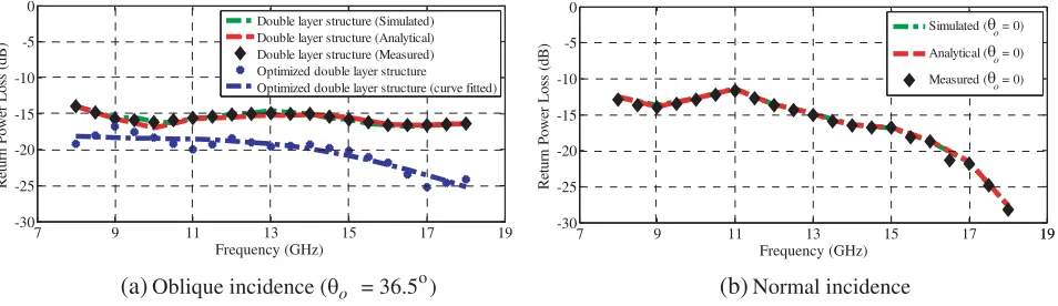
Figure 8 shows the free-space measurement of the return power loss (PL) of double layer absorber
backed with PEC as a manoeuvring target (θo = 36.5◦, θo = 0◦). A remarkable improvement in EM
wave absorption is fulfilled using the double-layer structure for both oblique and normal incident angles
shown in figure. The average value of obtained return power loss reached about −15.67 dB for oblique
incidence, while an average value of −18 dB was fulfilled in normal incidence case. It can be depicted
that good agreement is achieved among the measured, simulated, and analytical results for the double-layer structure. It is seen from the result that more than 90% from the incident wave was absorbed by the designed structure in case of an oblique incidence, while the return power loss reached up to
−28.32 dB in the case of normal incidence at 18 GHz. This means a big change in resistivity from front
layer to the backed metallic sheet provided by the designed structure. As shown in Fig. 8(a) for the oblique incidence, noticeable variations occur in the measured curves compared to the optimized curves due to the manufacturing process and the cost required for obtained precise manufactured sample. However, there are acceptable results as the overall performance of the measured samples fulfilled more than desired return power loss over the desired frequency range.
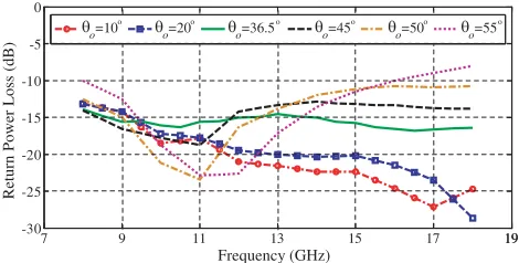
The performance of the designed absorber with different incidence angles has been studied as shown in Fig. 9. The figure illustrates the frequency response for obliquely incident TE polarized waves with
incidence angles of 10◦, 20◦, 36.5◦, 45◦, 50◦, and 55◦. It can be seen that the proposed absorber structure
can give a reflection coefficient less than−10 dB in the desired frequency range for the TE polarization
8 10 12 14 16 18
0 0.5 1 1.5 2 2.5 3
Relative permittivity & permeability
Optimized ε'
Optimized ε''
Optimized μ'
Optimized μ''
Final estimated ε'
Final estimated ε''
Final estimated μ'
Final estimated μ''
8 10 12 14 16 18
0 1 2 3 4 5 6 7 Frequency (GHz) R ela tive pe rm itt ivit
y & pe
rm
ea
bili
ty
Optimized ε'
Optimized ε''
Optimized μ'
Optimized μ''
Final estimated ε'
Final estimated ε''
Final estimated μ'
Final estimated μ''
Frequency (GHz)
(a) Matched layer (b) Lossy layer
Figure 7. Comparison between Optimized and final estimated (curve fitting) of relative dielectric and
permeability constants.
(a)Oblique incidence (θ = 36.5 ) (b)Normal incidence
7 9 11 13 15 17 19
-30 -25 -20 -15 -10 -5 0 Frequency (GHz)
Return Power Loss (dB)
Double layer structure (Simulated) Double layer structure (Analytical) Double layer structure (Measured) Optimized double layer structure Optimized double layer structure (curve fitted)
7 9 11 13 15 17 1919
-30 -25 -20 -15 -10 -5 0 Frequency (GHz)
Return Power Loss (dB)
Simulated (θo = 0)
Analytical (θ
o = 0)
Measured (θ
o = 0)
o
o
Figure 8. Free-space measurement of return power loss for TE polarization double layer absorber
7 9 11 13 15 17 1919 -30 -25 -20 -15 -10 -5 0 Frequency (GHz)
Return Power Loss (dB)
θo=10 θo=20 θo=36.5 θo=45 θo=50 θo=55
o o o o o o
Figure 9. Simulated frequency response of the
absorber for several angles of incidence for TE polarization.
7 9 11 13 15 17 19
-35 -30 -25 -20 -15 -10 -5 0 Frequency (GHz)
Return Power Loss (dB)
θo= 0 TE-mode
θo= 36. 5 TE-mode
θo= 0 TM-mode
θo= 36. 5 TM-mode (curve fitting)
θo= 36. 5 TM-mode
o
o
o
o
o
Figure 10. Simulated returns power loss for
incidence angles of interest (TM-mode) compared to TE-mode.
Table 3. Comparison between the proposed design and the previous published results.
Frequency Range (GHz)
Layers
PL (dB) Average value within the
entire bandwidth
Technique Layer
No.
Layer
Thickness Layer Construction
Overall Thickness
[5] 8−18 1 1.8 mm 85% MMP 2.6 mm 13 dB monostatic RCS
2 0.8 mm 10% carbon fiber
[8]
8−12
1 1.269 mm Ba (MnTi)2.7 Fe6.6 O19
5.015 mm 10 dB monostatic RCS
2 0.662 mm Ba (MnTi)1.6 Fe16 O27
3 1.262 mm Ba Co0.8 Ti0.8 Mn0.15Fe9.9O19
4 1.822 mm Ba (MnTi)1.7 Fe8.6O19
[9] 8 12.4
1 2. 5±0.5 mm Epoxy resin
7 mm 17 dB
bistatic RCS at incident angle 5 , TE monostatic RCS
2 0.5±0.5 mm MWCNTs 1%
3 0.97±.5 mm MWCNTs 2%
4 3±0.5 mm MWCNTs 3%
[11] 5.3 18 1 2.3 mm
Nano composite Ba Fe12 O19 /α-Fe
micro fibers 3.5 mm > − 20 dB monostatic RCS 2 1.2 mm α-Fe micro fibers
[10] 10.7:18
1 1.4 mm Nanocrystalline Alloy Fe0.2(Co0.2Ni0.8)0.8
2 mm
< −10 dB
(−71.4 dB at 12.1 GHz) monostatic RCS 2
0.6 mm
Nanocomposite SrFe12O19/Ni0.5Zn0.5Fe2O4
Microfibers
Our
work 8−18
1 2.5 mm
Natural rubber +(50% ferrimagnetic powders, 6.5% graphite and 1.5%
carbon fiber)
4 mm −16 dB (oblique incidence)
−18 dB (normal incidence)
bistatic RCS at incident angle 36. 5 ,
TE, monostatic RCS 2 1.5 mm Natural rubber + 45% high structure
of carbon fillers
− − − ≅ − ≅ − ≅ ≅ o o
with incidence angles up to 50◦. However, for incidence angle of 55◦, the required PL of −10 dB is
not achieved at the end of the desired bandwidth. This small deficiency in RCS results reduces the transmission loss factor inside the absorber structure to more than 80% for a frequencies from 16 to
18 GHz at angle of incident = 55◦.
Finally, Fig. 10 shows the absorber behavior in the case of TM incidence for angles of interest
(θo= 0◦ and 36.5◦) compared to simulated results of TE-RCS (dB). The figure shows that both TE and
TM polarizations yield the same magnitude of the reflection coefficient for normal incidence [24, 25]. For
incident angle of 36.5◦, the reflectivity is found to be around −10 dB for the desired bandwidth. The
Table 3 shows a comparison between the proposed design and previous published results. As depicted from the table, the proposed thin structure achieved better PL performance than the previously designed structures for both normal and oblique incidence waves within the entire bandwidth from 8 GHz to 18 GHz, using commercially available conductive, magnetic and dielectric materials.
5. CONCLUSION
In the current research work, the design of a compactly layered absorber over wide frequency range with both monostatic and bistatic RCS was fulfilled by tailoring both material properties and EM wave absorption mechanisms. The prediction of EM wave interaction properties of overall structure depends on the optimized properties of each layer besides the thickness, which are performed analytically and
by computational analysis resulting in a satisfied reflection losses for TE incidence up to −28.32 dB,
−17 dB for normal and oblique incidences, respectively. Potential EM wave absorption was achieved
in a structure contained the lossy sheet only backed by a metallic sheet, a remarkable improvement in EM wave absorption fulfilled with usage of a ferrite powder in the matching sheet tended to lower RF loss and higher power penetrated to a conductive lossy sheet. Predicted and experimentally results of material properties of each layer have been compared through three different methods to obtain precise values. Finally, EM wave absorption is examined using free-space method. The designed absorber
structure achieved a return power loss less than−10 dB in the desired bandwidth for the TE-mode with
incidence angle up to 50◦. In addition, the reflectivity is found to be around−10 dB in the case of TM
incidence for angles of interest.
ACKNOWLEDGMENT
Authors would like to acknowledge the Electronics Research Institute (ERI), Microstrip Department for the support and cooperation during simulations and measurements of this research.
REFERENCES
1. Huang, Y., Y. Feng, and T. Jiang, “Electromagnetic cloaking by layered structure of homogeneous
isotropic materials,” Optics Express, Vol. 15, No. 18, 11133–11141, 2007.
2. Yong, B.-Z. and T.-J. Cui, “Three-dimensional axisymmetric invisibility cloaks with arbitrary
shapes in layered-medium background,” Progress In Electromagnetics Research B, Vol. 27, 151–
163, 2011.
3. Perini, J. and L. S. Cohen, “Design of broad-band radar-absorbing materials for large angles of
incidence,”IEEE Transactions on Electromagnetic Compatibility, Vol. 35, No. 2, 223–230, 1993.
4. Attaf, B., Advances in Composite Materials — Ecodesign and Analysis, Chapter 13, 291–316,
InTech, 2011.
5. Gong, R., Y. He, X. Li, C. Liu, and X. Wang, “Study on absorption and mechanical properties of
rubber sheet absorbers,”Materials Science-Poland, Vol. 25, No. 4, 1001–1010, 2007.
6. Anyong, Q., “Design of thin wideband planar absorber using dynamic differential evolution and real
electromagnetic composite materials,” IEEE International Symposium, Antennas and Propagation
(APSURSI), 2912–2915, Spokane, WA, July 3–8, 2011.
7. Liang, W. M., Z. S. Jun, L. J. Qi, L. Wei, L. X. Mei, and X. W. Liang, “FSS design research
for improving the wide-band stealth performance of radar absorbing materials,”IEEE Proceeding,
International Work Shop, Metamaterials (Meta), 1–4, Nanjing, Oct. 2012
8. Ramesh, C., D. Singh, and N. K. Agarwal, “Implementation of multilayer ferrite radar absorbing
coating with genetic algorithm for radar cross-section reduction at X-band,” Indian Journal of
Radio and Space Physics, Vol. 36, No. 2, 145–152, 2007.
9. Micheli, D., R. Pastore, C. Apollo, M. Marchetti, G. Gradoni, V. M. Primiani, and F. Moglie,
“Broadband electromagnetic absorbers using carbon nanostructure-based composites,” IEEE
10. Li, M., W. Zhou, H. B. Liu, and X. Q. Shen, “Electromagnetic and microwave absorption
of nanocrystalline alloy Fe0.2 (Co0.2Ni0.8)0.8 and nanocomposite SrFe12O19/Ni0.5Zn0.5Fe2O4
microfibers,”Advanced Materials Research, Vol. 1035, No. 1033, 355–360, 2014.
11. Qian, S. X., L. H. Bo, W. Zhou, Q. X. Ye, J. M. Xiang, and Y. X. Chun, “Microwave absorption
properties of a double-layer absorber based on nanocomposite BaFe12O19/α-Fe and nanocrystalline
α-Fe microfibers,” Advanced Materials Research, Vol. 1035, 339–343, 2014.
12. Sukanta Das, G. C. N., S. K. Sahu, P. C. Routray, A. K. Roy, and H. Baskey, “Microwave absorption properties of double-layer RADAR absorbing materials based on doped Barium
Hexaferrite/TiO2/conducting carbon black,”Journal of Engineering, Vol. 2014, 1–5, 2014.
13. Sukanta Das, G. C. N., S. K. Sahu, P. C. Routray, A. K. Roy, and H. Baskey, “Microwave absorption properties of double-layer composites using CoZn/NiZn/MnZn-ferrite and titanium
dioxide,” Journal of Magnetism and Magnetic Materials, Vol. 377, 111–116, 2014.
14. John, L. W., “Broadband magnetic microwave absorbers: Fundamental limitations,” IEEE
Transactions on Magnetics, Vol. 29, No. 6, 4209–4214, 1993.
15. Knott, E. F., J. F. Shaffer, and M. T. Tuley, Radar Cross Section, Artech House, London, 1993.
16. Ghodgaonkar, D. K., V. V. Varadan, and V. K. Varadan, “Free-space measurement of complex
permittivity and complex permeability of magnetic materials at microwave frequencies,” IEEE
Transactions on Instrumentation and Measurement, Vol. 59, No. 2, 387–394, 1990.
17. Marina, Y. K., J. L. Drewniak, R. E. DuBroff, K. N. Rozanov, and B. Archambeault,
“Modeling of shielding composite materials and structures for microwave frequencies,” Progress
In Electromagnetics Research B, Vol. 15, 197–215, 2009.
18. Dharmendra, S., A. Kumar, S. Meena, and V. Agarwala, “Analysis of frequency selective surfaces
for radar absorbing materials,”Progress In Electromagnetics Research B, Vol. 38, 297–314, 2012.
19. Haupt, R. L., “An introduction to genetic algorithms for electromagnetics,”IEEE Transactions on
Antennas and Propagation Magazine, Vol. 37, No. 2, 7–15, 1995.
20. Morari, C., I. Balan, J. Pintea, E. Chitanu, and I. Iordache, “Electrical conductivity and electromagnetic shielding effectiveness of silicone rubber filled with ferrite and graphite powders,”
Progress In Electromagnetics Research M, Vol. 21, 93–104, 2011.
21. Nina, H., A. Vesel, V. Ivanovskiand, and M. K. Gunde, “Electrical conductivity of carbon black
pigments,”Dyes and Pigments, Vol. 95, No. 1, 1–7, Elsevier, 2012.
22. Queffelec, P., G. Philppe, J. Gieraltowski, and J. Loaec, “A microstrip device for the broad
band simultaneous measurement of complex permeability and permittivity,” IEEE Transactions
on Magnetics, Vol. 30, No. 2, 224–231, 1994.
23. William, W. B., “Automatic measurement of complex dielectric constant and permeability at
microwave frequencies,”IEEE Proceeding, Vol. 62, No. 1, 33–36, 1974.
24. Dib, N. I., M. Asi, and A. Sabbah, “On the optimal design of multilayer microwave absorbers,”
Progress In Electromagnetics Research C, Vol. 13, 171–185, 2010.
25. Roy, S., S. D. Roy, J. Tewary, A. Mahanti, and G. K. Mahanti, “Particle swarm optimization for
optimal design of broadband multilayer microwave absorber for wide angle of incidence,”Progress