Available online: https://edupediapublications.org/journals/index.php/IJR/ P a g e | 1374
An Analysis for Reduction of Communication Latency And
Power Consumption of NOCS
SHAIK MAHABOOB SUBAHAN1, SANKELLA JYOTSNA2
1Assistant Professor, Dept of ECE, Dr. K.V.SUBBA REDDY INSTITUTE OF TECHNOLOGY, Kurnool, AP.
2 M.Tech Dept of ECE, Dr.K.V.SUBBA REDDY INSTITUTE OF TECHNOLOGY, Kurnool, AP, India .
Abstract:
In this paper a New Hybrid scheme is proposed by combining packet switching and circuit switching to overcome the problems of packet switching and circuit switching. The Proposed
scheme provides high flexibility for
communications and also optimize latency of NoCs by establishing CS connections between communication pairs. It had been also demonstrated that establishing CS connections on the PS network can reduce communication power. This paper focuses on further reducing
the communication latency and power
consumption of NoCs, because the
communication latency of NoCs directly influences the data access latency in many-core systems, and the power consumption of NoCs accounts for a high ratio of the total power consumption of the whole chip
1. INTRODUCTION
Network-on-chip (NoC) has emerged as a scalable and promising technique to global communications within large multi middle structures. A bus arbiter controls get entry to the shared aid via granting get right of entry to to handiest one of the numerous soliciting for masters. There are several dangers associated with those sort of conversation architectures. Both factor-to-point as well as bus based conversation schemes aren't very scalable and can't correctly take care of the communications
requirements of contemporary SoC architectures. The overall performance of a bus degrades because the variety of requestors linked to the bus increases. This can be attributed to the fact that the bandwidth of the communique channel is shared among all of the bus requestors. This outcomes in the serialization of the requests to the bus, for this reason growing communique latencies. Also, the complexity and the delay of the arbiter increases as the range of requestors to the bus will increase. Technology scaling has brought on wire postpone to turn out to be a dominant thing of the general clock cycle time. Long wires in point-to-factor links as well as buses result in extended delays and are vulnerable to noise. Hence, on-chip communication using these schemes is becoming high priced in terms of both energy as well as velocity in the era of deep-submicron technology (DSM).
Fig: 1 bus, point to point, NoC communication
Available online: https://edupediapublications.org/journals/index.php/IJR/ P a g e | 1375
systems. NCOs help to accomplish the switch of
maximum quantity of facts between
communicating nodes within the least viable time. NCOs encompass routing factors related through small factor-to-factor links forming a records routing network on chip.
Unlike bus architectures, wherein the bus is occupied via one source node at some stage in the complete message transaction, the use of packet based communication in No allows for sharing of the hyperlinks among numerous speaking nodes. This will increase throughput and reduces communications latencies. NoC can be without problems scale by using connecting additional routing elements to the present community. The aggregate bandwidth of the network scales with growing community length. NCOs assist design reuse as the identical routing element can be used to scale the No to better
dimensions. This reduces the
time-to-marketplace and validation fees. Thus, NCOs provide a fairly ancient communication infrastructure for present day SoC and Multi middle architectures. Figure 1 indicates some examples of bus, factor-to-point and No based conversation architectures.
NoC Architecture and Components
A NoC includes routing nodes spread throughout a whole chip related collectively with the aid of communication hyperlinks A quick description of the numerous additives of the No is supplied below. Processing Elements (PEs) are the computational factors of the chip. These can be well known reason processor cores, digital sign processing cores, arithmetic common sense units, reminiscence cores or another specialised IP cores. They are the supply and the sink for all the data within the on-chip conversation network. Network Interfaces (NIs) join the processing elements to the principle on-chip communication community. They decouple the Computational
factors from the communique infrastructure. NIs convert the messages generated by means of the PEs into packets and insert additional routing facts based totally on the architecture of the below
Figure:2 NoC Architecture
lying network. Packets are decomposed into smaller devices called float manage gadgets or its which can be transmitted over the community. Flits are in addition categorised as head, body and tail its. The head it consists of the routing information required to course the packet to its destination. The head it allocates resources for the entire packet because it traverses from so urce to vacation spot. The frame and tail its bring most effective the packet payload without a routing facts and comply with the pinnacle it through the network. The tail it de-allocates the assets which have been allocate d to the packet with the aid of the head it. Routing Nodes are the coronary heart of the communique community.
Available online: https://edupediapublications.org/journals/index.php/IJR/ P a g e | 1376
transmission in every course. Links offer the bandwidth required for records transmission. In addition to the records transmission links, extra links required for control may also be present.
Figure 2 depicts these component s for a 4x4 NoC where the routing nodes connected as a grid. Network topology refers to the static association of routing nodes and links in an interconnection network. Selection of a great topology is essential to decrease the communication latency an d maximize the bandwidth. The routing and the drift manage schemes are heavily dependent on the form of the topology selected. Topologies may be
categorised into classes: ordinary
topologies and abnormal topologies The most typically used form of regular topology is the ok array n-cube . This topology includes N = okay N nodes organized as a normal n dimensional grid with ok nodes in every measurement linked by way of a pair of communique hyperlinks, one in every path. Each of the nodes can act as an enter or an output or a routing node. The maximum commonly used versions of the k-ary n-dice are the torus and mesh internet-works. Torus networks possess area symmetry.
II. PROPOSED HYBRID SCHEME BASED ON VIRTUAL CIRCUIT SWITCHING
The basic principle of the proposed hybrid scheme is that VCs are exploited in digital circuit switching to shape some of VCS
connections and more than one VCS
connections can share a commonplace physical
channel. In this hybrid scheme, VCS
connections cooperate with PS and CS
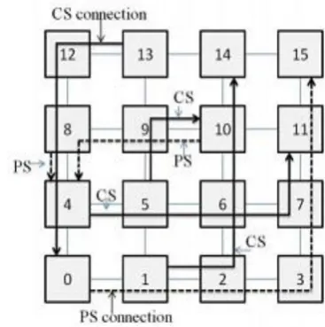
Fig.3 Simple traffic with communication routes in a 4 × 4 mesh.
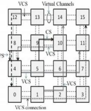
Available online: https://edupediapublications.org/journals/index.php/IJR/ P a g e | 1377 Fig 5. VCS, CS, and PS connections of the proposed
hybrid scheme.
Fig. 6 Router Architecture
connections at the same time, modified router architecture with five ports is proposed, as shown in Fig. 5. Compared with the baseline router, the additional hardware of the proposed router includes the bypass path, the circuit configuration, and the VCS state.
First, the bypass path is added in each input unit for allowing flits to go directly to the crossbar switch. Second, each input unit contains a PS
state and a VCS state. The PS state corresponds to the VC state of the baseline PS router, and the VCS state is used to support VCS connections. Third, the circuit configuration unit is to store the interconnect information for CS connections. In this paper, both the PS and the VCS states have n fields corresponding to n VCs. First, the VCS signal is only issued when crossbar switches of the VCS connection wait to be preconfigured. Due to the low activity of VCS signal, the power overhead caused by VCS signal can be much less than the power saving by bypassing buffer writing, routing, and arbitration of routers. Second, in the network with two VCs, the width of VCS signal is 2 bits in Virtual Circuit Switching. The proposed hybrid scheme supports the interweaving of packet switching, circuit switching, and virtual circuit switching. Two extra bits are added to each flit to denote the switching type of the flit. When a flit enters the router, these extra bits are checked at first. Then, the corresponding router pipeline is executed according to the switching type of the flit. This section mainly describes operations of virtual circuit switching. Note that VCS connections must be constructed in advance before the flit traveling in virtual circuit switching. Fig. 2 shows an example of traffic, in which physical channels (1, 2), (7, 11), and (8, 4) are shared by more than one communication, respectively. (x, y) denotes the physical channel from node x to node y. Fig. 3 shows CS connections and PS connections after using the conventional hybrid scheme. A CS connection is configured by recording in each router which input port should be connected to which output port. It is composed of physical channels and routers.
Available online: https://edupediapublications.org/journals/index.php/IJR/ P a g e | 1378
the ST stage. When there is no CS flit, the corresponding ports of crossbar switches are released to PS connections. Fig. 4 shows VCS, CS, and PS connections of the proposed hybrid scheme. A VCS connection comprises VCs and routers that have been configured by recording in each router which input VC should be connected to which downstream VC. Crossbar switches of routers are preconfigured during the SA stage before VCS flits require passing through. Because VCS connections are established over VCs, a physical channel can be shared by n VCS connections at most (n is equal to the VC number). Other communications competing for that physical channel must be executed in packet switching, such as the communication from node 8 to node 4 in Fig. 4.
III. OUTPUT WAVEFORMS
Fig 6: VCS signal input
Fig 7: VCS signal output
Fig 8: Switch allocation output
IV. CONCLUSION
In this paper, we present a novel hybrid scheme primarily based on digital circuit switching to further lessen communique latency and power of NoCs. The primary precept of the pro-posed hybrid scheme is to intermingle digital circuit switching with circuit switching and packet switching. Intermediate router pipelines are bypassed with the aid of organizing VCS connections and CS connections. A path allocation set of rules is also supplied to well allocate VCS connections and CS connections for a given traffic in mesh-linked NoCs, such that the average packet latency and electricity consumption are both optimized.
Available online: https://edupediapublications.org/journals/index.php/IJR/ P a g e | 1379
the fault tolerance, the quality-of-service (QoS) operation, the multicast delivery service, and the mapping, scheduling of applications based on virtual circuit switching.
REFERENCES
[1] Phi-Hung Pham, “Design and Implementation of an on-chip permutation network for
Multiprocessor System-on-Chip” IEEE
Transferee large scale integration (VLSI) systems,Vol.21.No.1, Page No-173- 177,January 2013.
[2] Bill Cordan, Palmchip Corporation An efficient bus architecture for system-on-chip design Custom integrated Circuits, 1999. [3] Sibabrata Ray, Hong Jiang. A reconfigurable
bus structure for multiprocessors with bandwidth reuse, Journal of Systems Architecture 45, 1999
[4] Hammond Lance, Olukotun Kunle.
Considerations in the Design of Hydra: A
Multiprocessor-on-a- Chip Micro
architecture, Stanford Technical Report CSL-TR-98-749, Stanford University, 1998.
[5] Lars-Hugo Hemert Digital kretsar, Student literature, Lund, 1996, ISBN 91-44-00099-5.
[6] John L. Hennessy, David A. Patterson Computer Architecture A Quantitative
Approach, second edition, Morgan
Kaufmann Inc, San Francisco California, 1996, ISBN 55860-329-8.
[7] Vincent P. Hearing & Harry F. Jordan Computer Systems Design and Architecture, Addison Wesley, California, 1997, ISBN 0-8053-4330-X.
[8] Howard Sachs, Mark Birnbaum VSIA
Technical Challenges Custom Integrated Circuits, 1999. Proceedings of the IEEE 1999 , 1999 , Page(s): 619 -622.
[9] Geert Rousseel, Sonics Inc. Decouple core for proper integration eeTimes Jan 3, 2000. www.eetimes.com.story/OEG20000103S004 8.
[10] Jon Turino, SynTest Technologies, Inc. emphDesign for Test and Time to Market -
Friends or Foes Test Conference, 1999. Page(s): 1098 -1101
About Authors:
Shaik Mahaboob Subahan, Assistant Professor in Dept. Of ECE, Dr.K.V.Subba Reddy Institute of Technology, Kurnool, AP, India.