NUST Publishing, © (2013), ISSN: 2070-9900
Interface Modification of Inverted Bulk Heterojunction Organic
Solar Cell by ZnO and CuO Layers
x1
School of Chemical and Materials Engineering, National University of Sciences and Technology, Islamabad 44000, Pakistan
2
Center for Energy Systems, National University of Sciences and Technology, Islamabad 44000, Pakistan
*Corresponding author: email- address; [email protected]
Abstract
The enhanced performance of the poly(3-hexylthiophene) (P3HT) and [6,6]-phenyl C61-butyric acid methyl ester (PCBM) bulk heterojunction devices was achieved by interface modification with solution processed ZnO and CuO x
interlayer. The highest power conversion efficiency (PCE) of 4.24±0.01% was achieved by optimizing the thickness of the interface layers by varyingspin coating speeds. The thin CuO layer improved both the short circuit current density x
2
(12.23mA/cm ) and fill factor (0.62) by providing additional light absorption through redistributing the electric field within the active layer.
The incident photon to current conversion efficiency (IPCE) was also improved to 67% by a 15nm thick CuO x
interlayer, showing that maximum carriers can be generated by optimizing the thickness of the amorphous CuO layer. x 2
The fabricated devices were characterized under 100mW/cm illumination and optical properties of each layer were also investigated.
Keyword: Organic solar cell, Interface modification, ZnO and CuO layers
Introduction
The development of bulk heterojunction (BHJ) organic photovoltaic (OPV) devices has attractedmore attention due to their potential advantages like low cost, flexibility, and large scale fabrication possibilities [1-6]. The regular structure of an OPV device is composed of a photoactive layer formed by a blend of an electron donor conjugated polymer and an electron acceptor fullerene derivatives. The active layer is sandwiched between two electrodes; anode is usually indium doped tin oxide (ITO) and cathode is a low work function metal cathode like Al [3,4 ,7]. Poly(3,4-ethylene dioxythiophene): (polystyrene sulfonic acid) (PEDOT:PSS) is most widely used interface material between ITO and active layer in regular structure. The device performance of this kind of structure is often degraded both by the instability of the PEDOT:PSS interface and oxidation of the cathode [8,9].
These challenges were addressed in the regular OPV device structure by inverting the device structure by replacing the low work function top electrode with a high work function metal electrode where electrons are accepted by ITO [10-12]. The inverted structure has improved device lifetime due to removal of PEDOT:PSSas its acidic nature always causes device instability. The other advantage of inverted configuration is vertical phase separation in BHJ which improved performance of the device[13].
The challenge in inverted devices is the selection of the electron accepting material and device design, so that this layer will not only affect the absorption of solar spectrum but also collect electrons and block holes efficiently. The energy level alignment in this regard is very crucial. There are various reports where diverse materials are used as an electron accepting material. The mostly used are zinc oxide (ZnO) [14-16], titanium oxide (TiO ) [17-20], cesium 2
carbonate (Cs CO ) [21-24]and lithium fluoride (LiF)[25].2 3
The interface layer of these materials is deposited by atomic layer deposition (ALD) [26,27 ], and sol–gel [28] techniques. The sol-gel process has the advantage of the solution process and low cost as no high temperature and vacuum are essential for the process.
The performance of the inverted OPV devices has lowered by the penetration of top electrodes into the active layer during thermal deposition and by the loss of the incident light due to reflection losses. These barriers are lowered by introducing a thin metal oxide interface layer between the active layer and the top electrode.
This study has focussed on the optimization of the thickness of the CuO interlayer for improved performance of inverted x
P3HT:PCBM BHJ devices. The various parameters like viscosity of the CuO sol and annealing temperature of the x
amorphous CuO layer was also optimized.x
Synthesis of ZnO and CuO layersx
ZnO solution was spin coated on ITO, which plays both roles- as an electron accepting layer and a hole blocking layer. The solution was prepared by dissolving 0.7M zinc acetate dehydrate in 2-methoxy ethanol, while 4% MEA was
o
also added during the stirring process at 60 C for two hours to get a homogenous solution. This solution was spin coated on ITO at 2800rpm for 35s, dried to hydrolysis at RT for one
o
hour and then annealed at 400 C for 5min. The spin coating conditions were optimized to get 25-40nm thin ZnO interface layer.
CuO solution was prepared by stirring a mixture of (0.25M) x
copper (II) acetate monohydrate dissolved in (99%)
o
isopropyl alcohol (IPA) and (1%) deionized water at 50 C for three hours. The solution was spin coated on active layer at various spin coating speeds for 35s, followed by annealing at
o
150 C for 10min.
1 2 2
Photovoltaic Devices Fabrication
The schematic and energy band diagram is shown in Figure 1.A 260nm thick photo-active layer was spin coated by P3HT:PCBM blend at 800rpm for 30s on the ZnO/ ITO substrate. The blend solution was obtained by dissolving (20mg/ml) P3HT and (15mg/ml) PCBM in chlorobenzene. An optimum blend ratio (1:1) was used in this particular study to obtain minimum P3HT grain size for maximum exciton dissociation in the active layer.
The thickness of the CuO layer on top of active layer was x
optimized by various spin coating speeds. Firstly, the solution was spin coated at 1200rpm to get 60nmthick CuOx layer. Then the second device was fabricated by spin coating thesolution on active layer at 1500rpm. The thickness of this layer was 35nm. Theother devices were fabricated by spin coating CuO solution at 1800rpm, 2100rpmand 2500rpm. x
The thickness of the resultant spacer layers were 20nm, 15nm and10nm, respectively. Ag was thermally evaporated as the top electrode on CuO optical spacer to complete the x
device structure. The various layers of the fabricateddevices are shown by FE-SEM in Fig2.
Results and Discussions
The high mobility metal oxide thin film provides enhanced carrier transport ascompared to organic material. The crystalline homogenous film of ZnO was obtainedafter
o
annealing at 400 C and confirmed by XRD analysis. The amorphousCuO film on top of active layer act as an optical x
spacer. The XRD analysis of CuO has shown that the film is x o
crystalline after annealing above 450 C.
The absorption and transmission spectra of ZnO indicate that most of thelight in the visible region has been allowed to be incident on the active layer, as shown in Fig 3. The maximum absorption by the blend is in the wavelength range475nm to 575nm and in this range the transmission by ZnO is more than 92%. Onthe other hand better absorption below 400nm by this layer has a positive effect ondevice performance by contributing increased generated carrier through absorptionwithin this wavelength range. The CuO optical x
spacer has 85% transmission inthe wavelength range above 400nm.
The photo-induced charge separation at the nano scale interface of the junction between the P3HT and PCBM occurs in sub-picosecond time – [7,29]. The photo luminescence spectroscopy, showing greatly quenched photo luminescence by P3HT:PCBM blend (Figure 4(a), and Figure 4©), and evidencing the enhancement of photoconductivity. The exciton quenching attributed by low luminescence intensity on introduction of CuO optical x
spacer shows that excitons are dissociated at blend CuO x
interface.
The J -V characteristic of the fabricated devices is shown in Figure 5. The effective work function of ITO and metal has beentuned by the application of ZnO and CuO inter layers x
respectively [30], which controlled the charge extraction fromthe active layer and therefore, short circuit current density (Jsc).The Jsc of the devices fabricated with CuOx spin
-2
coated at 1200rpm is minimum (8.22mAcm ).The
-2
Jscincreased to a maximum (12.23mAcm ) for the devices which werespin coated at 2100rpm by CuO . The increase in x
Fig 1:Schematic of the device design and energy band diagram of the materials used.
Fig 2: FE-SEM cross-sectional view of the device without top contact, the structure is
ITO/ZnO/ P3HT:PCBM/CuO .x
Fig 3: UV-Vis absorption and transmission spectrum of ZnO, ZnO spin coated on
Jsc is due to maximum carriercontribution when the thickness of the CuO optical spacer completely redistributesthe light x
distribution. However, as the rpm of optical spacer exceeds2500rpm Jscwas lowered. The possible explanation could be the penetration ofthe top electrode into the active layer as thin optical spacer has reduced protection from the damage during contact deposition. The increased thickness of the opticalspacer on the other hand has also increased the series resistance, which reducedthe Jsc,as observed for low rpm coated optical spacer.
The open circuit voltage (V ) of the devices fabricated with oc
high rpm CuO was reduced to 0.55 V compared to devices x
fabricated with thick spacer layer (1200rpm), havingV 0.58V. The introductionof interface layer oc
influences the energy level alignment at organic-organic andorganic-electrode interfaces [31-33] by introducing additional energy step. Therefore, the variation in V can be oc
attributedto the Fermi level pinning at the polymer-electrode interface.
The fill factor (FF) has improved from 0.58 to 0.62 as optical spacer thicknesswas reduced by higher rpm. The FF mainly depends upon the morphology ofthe active layer and the
series resistance of the devices [34-36]. The thickoptical spacer increased series resistance of the devices which has reduced the FF.
Fig 4:Photoluminscence spectrum of; (a) P3HT, P3HT:PCBM blend, ZnO/ P3HT:PCBM blend excited at 525nm; (b) PCBM excited at 320nm; (c) P3HT, P3HT:PCBM/ CuO , x
P3HT:PCBM blend excited at 500nm; (d) CuO excited at 320nm.x
P3HT:PCBMcUoX d
( c )
Figure 5: The J -V characteristic of the inverted organic photovoltaic devices fabricated with
The power conversion efficiency (PCE) of the devices was/isalso improved bythe introduction of ZnO thin layer on ITO, as the crystalline nature of this layersupports the electrons to reach the cathode quickly due to high mobility of ZnO.Whenever only cathode of the device is modified by high mobility metal oxide thenthere is possibility of space charge due to mobility difference of electron and holein metal oxide and polymer respectively. In order to overcome this challenge the introduction of metal oxide like CuO is a x
good choice. The PCE has improvedto 4.24±0.01% by spin coating CuO layer with a spin coating speed of 2100rpm on x
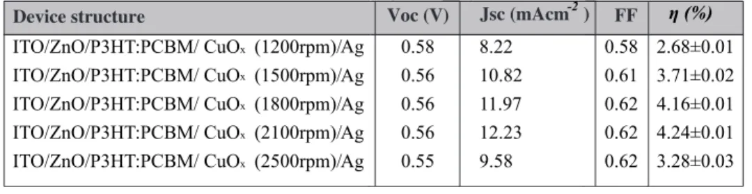
topof the photo-active layer. The structure of various fabricated devices and theirrespective parameters are presented in Table 1. The major contribution to theefficiency improvement is by Jsc and FF.
Figure 6 shows the incident photon to current conversion efficiency (IPCE)of devices fabricated by CuO optical x
spacer also act as a hole transport layer spincoated with different spin coating speed. 15nm thick CuO optical spacer x
spincoated at 2100rpm devices reached up to 67% at 530nm. However, thin opticalspacer (10nm) reduced IPCE to 58% though it is much higher than 35% shownby low rpm (1200rpm) coated optical spacer. The increased IPCE is evidencedthe increased photogenerated carrier contribution by a spacer layer through redistributing the field inside the active layer and by providing an efficient interfacebetween the anode and active layer.
Conclusions
The performance of the P3HT:PCBM BHJ devices was improved by interface modification with solution processed Z n O a n d C u O i n t e r l a y e r. T h e h i g h e s t P C E x
achieved(4.24±0.01%) by optimizing the thickness of the CuO interface layers at a spin coating speeds of 2100rpm. x
The thin CuO layer improved both the short circuit current x 2
density (12.23mA/cm ) and fill factor (0.62). The improved performance is attributed to the additional light absorption through redistributing the electric field within the active layer. The IPCE has also improved to 67% by a 15nm thick CuO interlayer, showing that maximum carriers can be x
generated and effectively collected by optimizing the thickness of the amorphous CuO layer. x
Acknowlegments
The authors acknowledge the financial support by Higher Education Commission of Pakistan (HEC) through out this study.
References
1. V.D.M. Paul W. M. Blom,L. Jan Anton Koster, and Denis E. Markov. Device Physics of Polymer:Fullerene Bulk Heterojunction Solar Cells. Advance Materials. Vol 19, 2007, pp. 1551- 1566.
2. S. Günes, H. Neugebauer, N.S. Sariciftci. Conjugated Polymer-Based Organic Solar Cells. Chem. Rev. Vol 107, 2007, pp.1324-1338.
3. G. Li, V. Shrotriya, J.Huang, Y. Yao, T. Moriarty, K. Emery, Y. Yang. "High-efficiency solution processable polymer photovoltaic cells by self-organization of polymer blends." Nat Mater. Vol 4, 2005, pp. 864-868. 4. J.Y. Kim, K. Lee, N.E. Coates, D. Moses, T.-Q. Nguyen,
M. Dante, A.J. Heeger. "Efficient Tandem Polymer Solar Cells Fabricated by All-Solution Processing". Science. Vol 317, 2007, pp. 222-225.
5. G. Dennler, M.C. Scharber, C.J. Brabec. Polymer-Fullerene Bulk-Heterojunction Solar Cells. Adv. Mater. Vol 21, 2009, pp. 1323-1338.
6. L.-M. Chen, Z. Hong, G. Li, Y. Yang. Recent Progress in P o l y m e r S o l a r C e l l s : M a n i p u l a t i o n o f Polymer:Fullerene Morphology and the Formation of Efficient Inverted Polymer Solar Cells. Adv. Mater. Vol 21, 2009, pp. 1434-1449.
7. H. Hoppe, N.S. Sariciftci. Morphology of polymer/fullerene bulk heterojunction solar cells. J. Mater. Chem. Vol. 16, 2006, pp. 45-61.
8. C.-Y. Li, T.-C. Wen, T.-H. Lee, T.-F. Guo, J.-C.-A. Huang, Y.-C. Lin, Y.-J. Hsu. "An inverted polymer
Table 1: The structure and the parameters of the fabricated inverted organic solar cells.
photovoltaic cell with increased air stability obtained by employing novel hole/electron collecting layers". J. Mater. Chem. Vol 19, 2009, pp. 1643-1647.
9 . M . J ø r g e n s e n , K . N o r r m a n , F. C . K r e b s . Stability/degradation of polymer solar cells. Sol. Energy Mater. Sol. Cells. Vol 92, 2008, pp. 686-714. 10. A.H. Muhammad Tanveer, Muhammad Bilal Khan. The
Inverted Double Heterojunction Organic Photovoltaic Devices using Electrospun TiO2
Nanofibers. International Journal of SoftComputing and Engineering. Vol 2, 2013, pp. 101-106.
11. M. Tanveer, A. Habib, M.B. Khan. "Improved efficiency of organic/inorganic photovoltaic devices by electrospun ZnO nanofibers". Materials Science and Engineering: B. Vol 177, 2012, pp. 144-1148.
12. J. You, C.-C. Chen, L. Dou, S. Murase, H.-S. Duan, S.A. Hawks, T. Xu, H.J. Son, L. Yu, G. Li, Y. Yang. Metal Oxide Nanoparticles as an Electron-Transport Layer in High-Performance and Stable Inverted Polymer Solar Cells. Adv. Mater. Vol 24, 2012, pp. 5267-5272.
13. Z. Xu, L.-M. Chen, G. Yang, C.-H. Huang, J. Hou, Y. Wu, G. Li, C.-S. Hsu, Y. Yang. Vertical Phase Separation in Poly(3-hexylthiophene): Fullerene Derivative Blends and its Advantage for Inverted Structure Solar Cells. Adv. Funct. Mater. Vol 19, 2009, pp. 1227-1234. 14. A.K.K. Kyaw, X.W. Sun, C.Y. Jiang, G.Q. Lo, D.W.
Zhao, D.L. Kwong. An inverted organic solar cell employing a sol-gel derived ZnO electron selective layer and thermal evaporated MoO[sub 3] hole selective layer. Appl. Phys. Lett. Vol 93, 2008, pp. 221107-221103.
15. J. Gilot, I. Barbu, M.M. Wienk, R.A.J. Janssen. The use of ZnO as optical spacer in polymer solar cells: Theoretical and experimental study. Appl. Phys. Lett. Vol 91, 2007, pp. 113520-113523.
16. M.S. White, D.C. Olson, S.E. Shaheen, N. Kopidakis, D.S. Ginley. Inverted bulk-heterojunction organic photovoltaic device using a solution-derived ZnO underlayer. Appl. Phys. Lett. Vol 89, 2006, pp. 143517-143513.
17. G.K. Mor, K. Shankar, M. Paulose, O.K. Varghese, C.A. Grimes. High efficiency double heterojunction polymer photovoltaic cells using highly ordered TiO[sub 2] nanotube arrays. Appl. Phys. Lett. Vol 91, 2007, pp. 152111-152113.
18. T. Kuwabara, C. Iwata, T. Yamaguchi, K. Takahashi. Mechanistic Insights into UV-Induced Electron Transfer from PCBM to Titanium Oxide in Inverted-Type Organic Thin Film Solar Cells Using AC Impedance Spectroscopy. ACS Applied Materials & Interfaces. Vol 2, 2010, pp. 2254-2260.
19. C. Waldauf, M. Morana, P. Denk, P. Schilinsky, K. Coakley, S.A. Choulis, C.J. Brabec. Highly efficient inverted organic photovoltaics using solution based titanium oxide as electron selective contact. Appl. Phys. Lett. Vol 89, 2006, pp. 233517-233513.
20. M.-H. Park, J.-H. Li, A. Kumar, G. Li, Y. Yang. Doping of the Metal Oxide Nanostructure and its Influence in
Organic Electronics. Adv. Funct. Mater. Vol 19, 2009, pp. 1241-1246.
21. G. Li, C.W. Chu, V. Shrotriya, J. Huang, Y. Yang. Efficient inverted polymer solar cells. Appl. Phys. Lett. Vol 88, 2006, pp. 253503-253503.
22. C.S. Kim, S. Lee, L.L. Tinker, S. Bernhard, Y.-L. Loo. Cobaltocene-Doped Viologen as Functional Components in Organic Electronics. Chem. Mater. Vol 21, 2009, pp. 4583-4588.
23. H.-H. Liao, L.-M. Chen, Z. Xu, G. Li, Y. Yang. Highly efficient inverted polymer solar cell by low temperature annealing of Cs[sub 2]CO[sub 3] interlayer. Appl. Phys. Lett. Vol 92, 2008, pp. 173303-173303.
24. J. Huang, G. Li, Y. Yang. A Semi-transparent Plastic Solar Cell Fabricated by a Lamination Process. Adv. Mater. Vol 20, 2008, pp. 415-419.
25. C.J. Brabec, S.E. Shaheen, C. Winder, N.S. Sariciftci, P. Denk. Effect of LiF/metal electrodes on the performance of plastic solar cells. Appl. Phys. Lett. Vol 80, 2002, pp. 1288-1290.
26. C.-Y. Chang, F.-Y. Tsai. Efficient and air-stable plastics-based polymer solar cells enabled by atomic layer deposition. J. Mater. Chem. Vol 21, 2011, pp. 5710-5715.
27. H. Cheun, C. Fuentes-Hernandez, Y. Zhou, W.J. Potscavage, S.-J. Kim, J. Shim, A. Dindar, B. Kippelen. Electrical and Optical Properties of ZnO Processed by Atomic Layer Deposition in Inverted Polymer Solar Cells†. J. Phys. Chem. C. Vol. 114, 2010, pp. 20713-20718.
28. Y. Sun, J.H. Seo, C.J. Takacs, J. Seifter, A.J. Heeger. Inverted Polymer Solar Cells Integrated with a Low-Temperature-Annealed Sol-Gel-Derived ZnO Film as an Electron Transport Layer. Adv. Mater. Vol 23, 2011, pp. 1679-1683.
29. B.C. Thompson, J.M. Fréchet. Polymer–fullerene composite solar cells. Angew. Chem. Int. Ed. Vol 47, 2007, pp. 58-77.
30. H.-L. Yip, S.K. Hau, N.S. Baek, H. Ma, A.K.Y. Jen. Polymer Solar Cells That Use Self-Assembled-Monolayer- Modified ZnO/Metals as Cathodes. Adv. Mater. Vol 20, 2008. pp. 2376-2382.
31. N.R. Armstrong, P.A.Veneman, E.Ratcliff, D. Placencia, M. Brumbach. Oxide Contacts in Organic Photovoltaics: Characterization and Control of Near-Surface Composition in Indium−Tin Oxide (ITO) Electrodes. Acc. Chem. Res.2009; 42: 1748-1757. 32. J. Hwang, A. Wan, A. Kahn. Energetics of metal–organic
interfaces: New experiments and assessment of the field. Materials Science and Engineering: R: Reports. Vol 64, 2009, pp. 1-31.
33. S. Braun, W.R.Salaneck, M.Fahlman. Energy-Level Alignment at Organic/Metal and Organic/Organic Interfaces. Adv. Mater. Vol 21, 2009, pp. 1450-1472. 34. M.-S. Kim, B.-G. Kim, J. Kim. Effective Variables To
35. T. Oo, N. Mathews, T. Tam, G. Xing, T. Sum, A. Sellinger, L. Wong, S. Mhaisalkar. Investigation of photophysical, morphological and photovoltaic behavior of poly (p-phenylene vinylene) based polymer/oligomer blends. Thin Solid Films. Vol 518,
2010, pp. 5292-5299.