VS-18TQ035-M3, VS-18TQ040-M3, VS-18TQ045-M3
www.vishay.com
Vishay Semiconductors
High Performance Schottky Rectifier, 18 A
FEATURES
• 175 °C TJ operation
• Low forward voltage drop
• High frequency operation
• High purity, high temperature epoxy
encapsulation for enhanced mechanical
strength and moisture resistance
• Guard ring for enhanced ruggedness and long term
reliability
• Designed and qualified according to JEDEC
®-JESD 47
• Material categorization: for definitions of compliance
please see
www.vishay.com/doc?99912
DESCRIPTION
The VS-18TQ... Schottky rectifier series has been optimized
for low reverse leakage at high temperature. The proprietary
barrier technology allows for reliable operation up to 175 °C
junction temperature. Typical applications are in switching
power supplies, converters, freewheeling diodes, and
reverse battery protection.
PRIMARY CHARACTERISTICS
IF(AV) 18 A
VR 35 V, 40 V, 45 V VF at IF 0.53 V IRM max. 25 mA at 125 °C
TJ max. 175 °C
EAS 24 mJ
Package 2L TO-220AC Circuit configuration Single
Anode
1 3
Cathode
Base
cathode 2
2L TO-220AC
MAJOR RATINGS AND CHARACTERISTICS
SYMBOL CHARACTERISTICS VALUES UNITS
IF(AV) Rectangular waveform 18 A
VRRM Range 35 to 45 V
IFSM tp = 5 μs sine 1800 A
VF 18 Apk, TJ = 125 °C 0.53 V
TJ Range -55 to +175 °C
VOLTAGE RATINGS
PARAMETER SYMBOL VS-18TQ035-M3 VS-18TQ040-M3 VS-18TQ045-M3 UNITS
Maximum DC reverse voltage VR
35 40 45 V
Maximum working peak reverse voltage VRWM
ABSOLUTE MAXIMUM RATINGS
PARAMETER SYMBOL TEST CONDITIONS VALUES UNITS
Maximum average forward current,
see fig. 5 IF(AV) 50 % duty cycle at TC = 149 °C, rectangular waveform 18
A Maximum peak one cycle
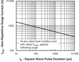
non-repetitive surge current, see fig. 7 IFSM
5 μs sine or 3 μs rect. pulse Following any rated load condition and with rated VRRM applied
1800 10 ms sine or 6 ms rect. pulse 390
Non-repetitive avalanche energy EAS TJ = 25 °C, IAS = 3.6 A, L = 3.7 mH 24 mJ Repetitive avalanche current IAR
Current decaying linearly to zero in 1 μs
Frequency limited by TJ maximum VA = 1.5 x VR typical
VS-18TQ035-M3, VS-18TQ040-M3, VS-18TQ045-M3
www.vishay.com
Vishay Semiconductors
Note
(1) Pulse width < 300 μs, duty cycle < 2 %
ELECTRICAL SPECIFICATIONS
PARAMETER SYMBOL TEST CONDITIONS VALUES UNITS
Maximum forward voltage drop
See fig. 1 VFM (1)
18 A
TJ = 25 °C
0.60
V
36 A 0.72
18 A
TJ = 125 °C
0.53
36 A 0.67
Maximum reverse leakage current
See fig. 2 IRM(1)
TJ = 25 °C
VR = Rated VR
2.5
mA
TJ = 125 °C 25
Maximum junction capacitance CT VR = 5 VDC (test signal range 100 kHz to 1 MHz) 25 °C 1400 pF Typical series inductance LS Measured lead to lead 5 mm from package body 8 nH Maximum voltage rate of change dV/dt Rated VR 10 000 V/μs
THERMAL - MECHANICAL SPECIFICATIONS
PARAMETER SYMBOL TEST CONDITIONS VALUES UNITS
Maximum junction and storage
temperature range TJ, TStg -55 to +175 °C
Maximum thermal resistance,
junction to case RthJC DC operationSee fig. 4 1.50
°C/W Typical thermal resistance,
case to heatsink RthCS Mounting surface, smooth, and greased 0.50
Approximate weight 2 g
0.07 oz.
Mounting torque minimum 6 (5) kgf · cm(lbf in)
maximum 12 (10)
Marking device Case style 2L TO-220AC
18TQ035 18TQ040 18TQ045
VS-18TQ035-M3, VS-18TQ040-M3, VS-18TQ045-M3
www.vishay.com
Vishay Semiconductors
Fig. 1 - Maximum Forward Voltage Drop Characteristics Fig. 2 - Typical Values of Reverse Current vs. Reverse Voltage
Fig. 3 - Typical Junction Capacitance vs. Reverse Voltage 1000
100
10
1
VFM - Forward Voltage Drop (V)
IF
- Instantaneous Forward Current (A)
0 0.1
1.4 0.2 0.4 0.6 0.8 1.0 1.2
TJ = 25 °C TJ = 175 °C TJ = 125 °C
1.6
IR
- Reverse Current (mA)
VR - Reverse Voltage (V)
0 10 20 30 40 50
0.0001 0.001 0.01 0.1 1 10 100 1000
TJ = 125 °C TJ = 175 °C TJ = 150 °C
TJ = 100 °C TJ = 75 °C TJ = 50 °C
TJ = 25 °C
CT
- Junction Capacitance (pF)
VR - Reverse Voltage (V)
0 10 20 30 40 50
100 10 000
1000
t1 - Rectangular Pulse Duration (s)
ZthJC
- Thermal Impedance (°C/W)
0.001
0.01 0.1 1 10
0.00001 0.0001 0.001 0.01 0.1 1 10 100
D = 0.50 D = 0.33 D = 0.25 D = 0.17 D = 0.08
Single pulse
(thermal resistance) .
.
PDM
t1 t2
Notes:
1. Duty factor D = t1/t2 2. Peak TJ = PDM x ZthJC + TC
VS-18TQ035-M3, VS-18TQ040-M3, VS-18TQ045-M3
www.vishay.com
Vishay Semiconductors
Fig. 5 - Maximum Allowable Case Temperature vs. Average Forward Current
Fig. 6 - Forward Power Loss Characteristics
Fig. 7 - Maximum Non-Repetitive Surge Current
Fig. 8 - Unclamped Inductive Test Circuit IF(AV) - Average Forward Current (A)
Allowable Case Temperature (°C)
150 155 160 165 170 175 180
DC
0 4 8 12 16 20 24 28
18TQ
RthJC (DC) = 1.50 °C/W
IF(AV) - Average Forward Current (A)
Average Power Loss (W)
0 4 8 12 16 20 24 28
0 5 10 15
RMS Limit D = 0.08
D = 0.17 D = 0.25 D = 0.33 D = 0.50
DC
tp - Square Wave Pulse Duration (µs) IFSM
- Non-Repetitive Surge Current (A)
10 100 1000 10 000
100 1000 10 000
At any rated load condition and with rated VRRM applied
following surge
Current monitor
High-speed switch D.U.T.
Rg = 25 Ω
+ Freewheel
diode Vd = 25 V L
IRFP460
VS-18TQ035-M3, VS-18TQ040-M3, VS-18TQ045-M3
www.vishay.com
Vishay Semiconductors
ORDERING INFORMATION TABLE
ORDERING INFORMATION (Example)
PREFERRED P/N QUANTITY PER T/R MINIMUM ORDER QUANTITY PACKAGING DESCRIPTION
VS-18TQ035-M3 50 1000 Antistatic plastic tube
VS-18TQ040-M3 50 1000 Antistatic plastic tube
VS-18TQ045-M3 50 1000 Antistatic plastic tube
LINKS TO RELATED DOCUMENTS
Dimensions www.vishay.com/doc?96156
Part marking information www.vishay.com/doc?95391
SPICE model www.vishay.com/doc?96209
2
-
Current rating (18 = 18 A)
3
-
Package:
T = TO-220
4
-
Schottky “Q” series
5
-
Voltage ratings
6
035 = 35 V
040 = 40 V
045 = 45 V
Device code
6
2
3
4
5
18
T
Q
045
-M3
1
VS-1
-
Vishay Semiconductors product
--M3 = halogen-free, RoHS-compliant, and termination lead (Pb)-free
Environmental digit
Outline Dimensions
www.vishay.com
Vishay Semiconductors
2L TO-220AC
DIMENSIONS
in millimeters and inches
Notes
(1) Dimensioning and tolerancing as per ASME Y14.5M-1994
(2) Lead dimension and finish uncontrolled in L1
(3) Dimension D, D1, and E do not include mold flash. Mold flash shall not exceed 0.127 mm (0.005") per side. These dimensions are measured
at the outermost extremes of the plastic body
(4) Dimension b1, b3, and c1 apply to base metal only
(5) Controlling dimensions: inches
(6) Thermal pad contour optional within dimensions E, H1, D2, and E1
(7) Outline conforms to JEDEC® TO-220, except D2
SYMBOL MILLIMETERS INCHES NOTES SYMBOL MILLIMETERS INCHES NOTES
MIN. MAX. MIN. MAX. MIN. MAX. MIN. MAX.
A 4.25 4.65 0.167 0.183 D2 11.68 13.30 0.460 0.524 6, 7
A1 1.14 1.40 0.045 0.055 E 10.11 10.51 0.398 0.414 3, 6
A2 2.50 2.92 0.098 0.115 E1 6.86 8.89 0.270 0.350 6
b 0.69 1.01 0.027 0.040 e 2.41 2.67 0.095 0.105
b1 0.38 0.97 0.015 0.038 4 e1 4.88 5.28 0.192 0.208
b2 1.20 1.73 0.047 0.068 H1 6.09 6.48 0.240 0.255 6
b3 1.14 1.73 0.045 0.068 4 L 13.52 14.02 0.532 0.552
c 0.36 0.61 0.014 0.024 L1 3.32 3.82 0.131 0.150 2
c1 0.36 0.56 0.014 0.022 4 Ø P 3.54 3.91 0.139 0.154
D 14.85 15.35 0.585 0.604 3 Q 2.60 3.00 0.102 0.118
D1 8.38 9.02 0.330 0.355
1 2
C C
D D
2 x b2 2 x b
(b, b2)
b1, b3 0.014MBAM
0.015MBAM
Conforms to JEDEC® outline TO-220AC (6)
(6)
(6)
L1 (2)
Detail B
Section C - C and D - D Base metal Plating
(4)
(4) c1 c
(6)
(6) Ø P
E
Q
D
L c D1
e
e1 2 x
A
B A
A
A C A2
A1
Thermal pad
H1
(E)
(H1)
D2
Detail B
E1
View A - A