AUSTRALIAN JOURNAL OF BASIC AND
APPLIED SCIENCES
ISSN:1991-8178 EISSN: 2309-8414 Journal home page: www.ajbasweb.com
Open Access Journal
Published BY AENSI Publication
© 2017 AENSI Publisher All rights reserved
This work is licensed under the Creative Commons Attribution International License (CC BY). http://creativecommons.org/licenses/by/4.0/
To Cite This Article: Avneet Kaur and Chanpreet Kaur Toor., Implementation of Parallel Prefix Adders Using FPGA’S. Aust. J. Basic & Appl. Sci., 11(8): 100-106, 2017
Implementation of Parallel Prefix Adders Using FPGA’S
1Avneet Kaur and 2Chanpreet Kaur Toor
1Student, Electronics and Communication Engineering, Chandigarh Engineering College Landran, Avneet Kaur Ludhiana, Punjab.
2Assistant professor Electronics and Communication Engineering, Chandigarh Engineering College Landran, ECE (VLSI Design)
Chanpreet Kaur Toor Chandigarh, Punjab.
Address For Correspondence:
Avneet Kaur, Student, Electronics and Communication Engineering, Chandigarh Engineering College Landran, Avneet Kaur Ludhiana, Punjab.
A R T I C L E I N F O A B S T R A C T Article history:
Received 18 February 2017 Accepted 15 May 2017
Available online 18 May 2017
Keywords:
PPA –Parallel –prefix adders, FPGA- Field Programmable Gate Arrays, CSA- Carry Skip Adder, RCA- Ripple Carry Adder, SKS-Sparse Kogge Stone.
Objectives: This paper examines three variations of carry-tree adders (spanning tree adder, sparse Kogge-Stone & Kogge-Stone adder) and presents a comparison with Carry Skip Adder (CSA) & simple Ripple Carry Adder (RCA). Methods/Statistical Analysis: In VLSI designs the best performance can be obtained from Parallel-prefix adders (PPA) which are also termed as carry tree adders. Due to constraints on routing overhead & logic block configurations the advantage in performance in FPGA executions doesn't translate directly. Xilinx Spartan 3E FPGA is used to implement these designs which has varied bit-widths & the -performance logic analyzer is used for delay dimensions. Findings: Better delay performance is observed by the RCA designs of 128 bits due to the use of fast carry-chain. As in the case of carry-tree adders having bit widths of 256 bits there is a speed advantage over the RCA. RCA is the most commonly used adder implemented using full and half adders. As RCA is a serial adder which can perform any no. of additions but due to carry propagation there is a problem of propagation delay from stage to stage. PPAs are used to overcome delay problem as the carry is pre-computed. Various PPAs are Spanning tree, SKS adder, KS adder and Brent kung adders. Improvements: By using delay and power controls, design and comparison between these adders performed. Xilinx ISE software is used for synthesis process & simulation of these adders and results are presented in this paper.
INTRODUCTION
In the binary addition unit, the main component in the majority digital path classes together with digital signal processors as well as micro chip find out passageway units. Generally, severe examination carries on being beneath fire at rising the capability holdup time of the adder (Hoe, D.H.K., et al., 2011). Reconfigurable logics such as Field Programmable Gate Arrays are most popular from the past few years and are latest in technology. As significance, it provides us with the benefits of improved rate and power for DSP and microprocessor based resolutions for abundant reasonable styles including mobile DSP as well as telecommunications applications as well as a deep degradation in progress time as well as price on to Application Specific computer circuit designs. The skill benefit is mainly key with the increasing value of mobile as well as portable physical science, which causes austere use of DSP functions (Yezerla, S.K. and B. Rajendra Naik, 2014).
adders on Field Programmable Gate Arrays are labeled. Assistant degree in luxurious testing criteria for contrasting the feat of those adders is described (Roy, S., et al., 2014). Numerous tree-based adder designs are compulsory and featured on a Field Programmable Gate Arrays as well as estimated with the Ripple Carry Adder as well as also the Carry Skip Adder.
Parallel Prefix Adders:
The PPA is sort of a Carry Look Ahead Adder. The prefix adders will be designed in a number of different ways that endured the innumerable wants. There is a bent to use tree structure sort for expanding the quickness of process. Parallel prefix adders are faster adders and these are rapider adders. They are used for major presentation arithmetic structures in trades and assemblies (Zode, P.P. and R.B. Deshmukh, 2014; Escobar, K.A. and R.P. Ribas, 2013). The parallel prefix addition is completed in three steps.
A. Pre-Processing Stage:
In this stage we are inclined to work out, produce and broadcast signals. Carry input of every adder is generated (Nehru, K., A. Shanmugam and S. Vadivel, 2012). A and B are the inputs. These signals are given by the equation 1& 2.
(1)
(2)
B. Carry Generation Network:
In this step there is similarity to work out carries such as every bit. Achievement is finished in parallel type (Martinez, C.D., et al., 2012). When the working out of carries is in parallel, they're divided into smaller items. Carry operator contain 2 AND gates, one OR gate. It practices, propagate and generate as midway signals that are given by the equations 3& 4.
(3)
(4)
Fig. 1: Carry Operator
C. Post Process Stage:
This is the final period to work out the neglected of input bits. This is similar for all adders. The add bit equation given
(5)
(6)
Proposed Methodology:
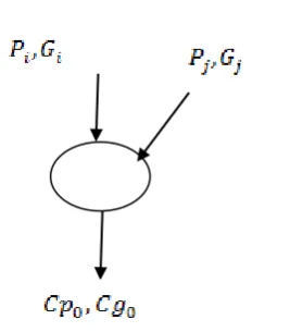
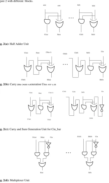
block is the mutual block for both the carry ‘1’ and ‘0’ mathematical calculation. The methodology is shown in figure 2 with different blocks.
Fig. 2(a): Half Adder Unit
Fig. 2(b): Carry and Sum Generation Unit for Cin
Fig. 2(c): Carry and Sum Generation Unit for Cin_bar
Fig. 2(d): Multiplexer Unit
…
b(0) b(0)
a(n) a(n)
Ci(n) Si(n) Ci(0) Si(0)
Ci(n) Si(n) C1(n-1)
S1(n) C1(n)
C1(0) Ci(0) Si(0) Cin
S1(0)
…
S1(n) S0(n) Cin S1(0) S0(0) Cin
S(n) S(0)
…
Cin Si(0)
Ci(0) C0(0)
S0(0) S0(n)
C0(0)
C0(n-1) Si(n)
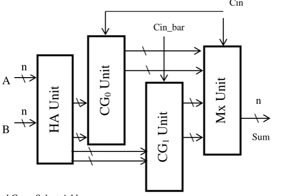
Fig. 2(e): Proposed Carry Select Adder
In figure 2(e), the proposed CSLA is shown. The division of adder architecture into 4 sub blocks is shown in figure 2(a)- 2(d). In the first block the simple half adder is used which figures the sum and carry value which is shown in figure 2(a). is used for sum calculation and is used for carry output. The Half adder sum and carry output equations are
Si = a xor b Ci = a and b
In the second block Carry and Sum generation is realized which after taking the output from the first unit generates the sum and carry values ( used for carry and sum respectively) for input carry . The whole architecture behaves like a full adder realized using two half adder blocks. The output of the sum and carry are produced using
S0 = Si xor Ci
C0 = (Si and Cin) or Ci
The third block also behaves like a full adder. It shares the common half adder resources from the first block and after that generates the carry and the sum( for carry and sum of this block respectively) for carry input as bar. Finally in the fourth block, the mux architecture is implemented and is shown in figure 2(d). It selects one of the outputs from the second and third block. The final sum is generated by using the equation
S = (S0 and not Cin) or (S1 and Cin)
RESULTS AND DISCUSSIONS
The proposed technique is executed using the Xilinx Spartan 3 FPGA and Verilog language is used for the implementation of the design. The technique is associated with the basic RCA approach and the results shows an enhancement in both the area consumed by the device and the maximum combinational path delay. In Table 1 the comparison of both the approaches is shown on the basis of various performance parameters like number of slices, number of look up tables, delay and maximum operating frequency. Number of slices, number of 4 input LUTs are a amount of the number of resources used by the FPGA which comes out to be less in case of the proposed approach.
Table 1: Comparison Table
Parameters Basic Approach Proposed Approach
Number of Slices 52 46
Number of 4 Input LUTs 92 81
Number of Bonded IOs 101 101
Delay (ns) 33.166 21.913
Max. Frequency (MHz) 30.15 45.63
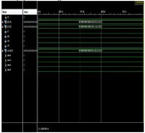
While delay is the measure of the speed of design which also comes out to be less as compared to the basic approach. Figure 3 shows the top level module and RTL view of the methodology which is proposed and figure 4 shows the simulation waveform. It is lucid from the comparison chart that the proposed methodology utilizes less area in comparison with the basic ripple carry adder. The performance is faster and decreases the maximum combinational path delay of the carry select adder.
Fig. 3: RTL Schematic of the proposed Methodology
The graph shows the comparison outcomes in figure 5 and 6. The comparison of the area utilization by the device is shown in figure 5 and in figure 6 the proposed delay improvement is shown. Figures show the comparison of data shown in table 1. It is clear from the figure 5 that the proposed approach utilizes lesser area as compared to the basic approach. It is shown in terms of number of slices and number of 4 input LUTs. Figure 5 shows the comparison of combinational path delay which is the measure of the speed of the design the minimum delay, the maximum speed and it is clear from the graph that proposed approach has less delay and maximum operating frequency as compared to the basic approach.
Fig. 5: Comparison of Area Utilization
Fig. 6: Comparison of Delay
Conclusion:
Arithmetic unit is the most widely researched and used designs in the digital electronics circuits. Many researchers in recent past have proposed different approaches for the design of adders and other logical circuits and compared their merits and demerits with the existing approaches. Parallel prefix adder is designed in this approach by using optimized CSLA in terms of area and speed. In the proposed approach carry select adder is planned with the help of logical gates for reducing the area consumed by the adder. It is shown from the results that the proposed approach outperform the basic approach on the basis of both area and delay of the design.
REFERENCES
Yezerla, S.K. and B. Rajendra Naik, 2014. "Design and estimation of delay, power and area for Parallel prefix adders," 2014 Recent Advances in Engineering and Computational Sciences (RAECS), Chandigarh, pp: 1-6. Doi: 10.1109/RAECS.2014.6799654.
Roy, S., M. Choudhury, R. Puri and D.Z. Pan, 2014. "Towards Optimal Performance-Area Trade-Off in Adders by Synthesis of Parallel Prefix Structures," in IEEE Transactions on Computer-Aided Design of
Integrated Circuits and Systems, 33(10): 1517-1530.
Zode, P.P. and R.B. Deshmukh, 2014. "Fast modular multiplication using parallel prefix adder," 2014 2nd
International Conference on Emerging Technology Trends in Electronics, Communication and Networking,
Surat, pp: 1-4.
Escobar, K.A. and R.P. Ribas, 2013. "Parallel prefix adder design using quantum-dot cellular automata," 2013 26th Symposium on Integrated Circuits and Systems Design (SBCCI), Curitiba, pp: 1-6.
Nehru, K., A. Shanmugam and S. Vadivel, 2012. "Design of 64-bit low power parallel prefix VLSI adder for high speed arithmetic circuits," 2012 International Conference on Computing, Communication and
Applications, Dindigul, Tamilnadu, pp: 1-4. Doi: 10.1109/ICCCA.2012.617920.
Martinez, C.D., L.P.D. Bollepalli and D.H.K. Hoe, 2012. "A fault tolerant parallel-prefix adder for VLSI and FPGA design," Proceedings of the 2012 44th Southeastern Symposium on System Theory (SSST), Jacksonville, FL, pp: 121-125. Doi: 10.1109/SSST.2012.619514.
Uma, R. and J. Ponnian, 2012. "Systolic FIR Filter Design with Various Parallel Prefix Adders in FPGA: Performance Analysis," 2012 International Symposium on Electronic System Design (ISED), Kolkata, pp: 111-115. Doi: 10.1109/ISED.2012.45.
Das, S. and S.P. Khatri, 2008. "A Novel Hybrid Parallel-Prefix Adder Architecture With Efficient Timing-Area Characteristic," in IEEE Transactions on Very Large Scale Integration (VLSI) Systems, 16(3): 326-331, Doi: 10.1109/TVLSI.2007.91550.
Liu, J., Y. Zhu, H. Zhu, C.K. Cheng and J. Lillis, 2007. "Optimum Prefix Adders in a Comprehensive Area, Timing and Power Design Space," 2007 Asia and South Pacific Design Automation Conference, Yokohama, pp: 609-615. Doi: 10.1109/ASPDAC.2007.358053.
Haikun Zhu, Chung-Kuan Cheng and R. Graham, 2005. "Constructing zero-deficiency parallel prefix adder of minimum depth," Proceedings of the ASP-DAC 2005. Asia and South Pacific Design Automation
Conference, 2: 883-888 Doi: 10.1109/ASPDAC.2005.1466481.
Moghaddam, M. and M.B. Ghaznavi-Ghoushchi, 2011. "A new low power-delay-product, low-area, parallel prefix adder with reduction of graph energy," 2011 19th Iranian Conference on Electrical Engineering, Tehran, pp: 1-6.
Uma, R. and J. Ponnian, 2012. "Systolic FIR Filter Design with Various Parallel Prefix Adders in FPGA: Performance Analysis," 2012 International Symposium on Electronic System Design (ISED), Kolkata, pp: 111-115. Doi: 10.1109/ISED.2012.45.
Zarandi, A.A.E., A.S. Molahosseini, M. Hosseinzadeh, S. Sorouri, S. Antão and L. Sousa, 2015. "Reverse Converter Design via Parallel-Prefix Adders: Novel Components, Methodology, and Implementations," in IEEE
Transactions on Very Large Scale Integration (VLSI) Systems, 23(2): 374-378.
Doi: 10.1109/TVLSI.2014.2305392.
Krishna Kumari, V., Y. Sri Chakrapani, Dr. M. Kamaraju, 2013. “Design and Characterization of Kogge stone, Sparse Kogge stone, Spanning tree and Brent kung Adders” International Journal of Scientific & Engineering Research, 4: 10.