ISSN 1990-9233
© IDOSI Publications, 2014
DOI: 10.5829/idosi.mejsr.2014.22.08.21987
Securing Logic Circuits Using Run-Time Programmable Interconnection Network
Binu K. Mathew and K.P. Zacharia1 2
Research Scholar, Anna University, Chennai, Tamil Nadu, India 1
Electronics & Communication, SAINTGITS College of Engineering, Kottayam, Kerala, India 2
Abstract: Security of digital hardware against various possible attacks is a major issue in today’s world. Various researchers all over the world had proposed several FPGA threat models and proposed several solutions and methodologies to fight against these threat models. Cryptographic techniques are commonly used to keep digital systems secure and robust against various types of attacks. Cryptography increases system security as well as complexity and cost of the system as well. This paper proposes a new system without using cryptography to secure digital systems against possible threat models by using 8 input 8 output Secured Programmable Interconnection Network (SPIN8X8). This network defines an interconnection pattern between two logic blocks in a digital system and the interconnection pattern is based on the interconnection pattern code applied by the user at run-time. Finally a SPIN array is explained which is based on SPIN8X8 network, which can be used to interconnect different blocks of a system.
Key words: Interconnection Network Programmable Interconnection Secured Devices Programmable Circuits SPIN
INTRODUCTION SPIN is dependant on the interconnection pattern code Digital devices and circuits particularly systems SPIN network in the proper manner, if and only if based on FPGA are prone to various types of attacks as proposer IPC is applied to the SPIN. In other words, for estimated by various researchers from different parts of each interconnection code defined, blocks are the world. Among these, most widely found threat interconnected in a particular pattern which is defined by models are bit-stream cloning, altering the FPGA bit- the SPIN designer.
stream and unauthorized usage of the FPGA based Present day digital systems rely on cryptographic system. Researchers had proposed various cryptographic systems to protect the bit-steams of the FPGA from techniques to fight against these FPGA threat models. various types of attacks proposed by various These techniques increase system security as well as cost researchers. These are not suitable for small less complex and complexity of the system. Due to this reason, systems, as more resources will be used by the cryptographic techniques are not preferred for low cost, cryptographic blocks and fewer blocks will be used by less complex digital systems. Cryptography based the actual logic system. Even with cryptography, logic systems also increases cost as well as size of the digital systems with less number of inputs are not secure, as a system. This paper proposes a new technique to enhance modern computer can find the relationship between security of a logic system by simply dividing the circuits outputs and inputs of the system. For an intruder it is not into two sub-circuits and connect these circuits using a so difficult to develop the bit-steam with the aid of a Secured Programmable Interconnection Network (SPIN). computer with good configuration. A Secured For the proposed system, as there are 8 inputs and 8 Programmable Interconnection Network (SPIN) can be outputs this circuit is called as SPIN8X8. An array of the used to secure different logic circuits by not defining proposed circuits, called as SPIN array, can be used to an interconnection between different parts of the increase the degree of security of a system. The digital system. A trespasser who is trying to trespass interconnection pattern for two blocks defined by the into the system will enter various interconnection (IPC) of that SPIN. Two blocks are connected using the
patterns and the proposed system provides an can enhance the security of integrated circuits making it interconnection between various blocks for each pattern robust against different types of attacks. A barrier is applied. Even by trial and error method, an intruder cannot introduced between input lines and various blocks of the find the actual interconnection as for every pattern code logic circuit when a wrong key is applied. Ishai et al. [11] applied, there is an interconnection pattern defined for the had reported that even cryptosystems are prone to side
SPIN network. channel attacks (SCA) and proposed that incorporating
Rest of the paper is organized as follows; literature private circuits will enhance security of logic circuits survey is discussed in Section 2. Architecture of 8-input, against side channel attacks. Authors of [12] had reported 8-output programmable interconnection network a fast and secure chaos based encryption system using (SPIN8X8) and a SPIN array for secured logic circuits is digital logic system which is much more efficient and explained in Section 3. A motivational example using superior than the existing system. In his work, Chaves [13] proposed system is explained in section 4 and Section 5 had reported that use of a secure computing module will explains how this system enhances security of a system. enhance the security of conventional cryptographic Section 6 discusses experimental results of the proposed systems by 5 times. In [14] Jensen et al. had proposed a system and conclusive remarks and future work is secure reconfigurable computing architecture for explained in Section 7. multi-user environment. A survey of possible approaches Literature Survey: The evolution of secured devices had circuits is discussed by its authors in [15]. Zheng and started long back since the evolution of re-programmable Potkonjak in [16] had proposed a technique to secure devices like FPGAs. Researchers had proposed several net-list level FPGA design through process variation and techniques to protect the design of a digital circuit from degradation. Rajendran et al[17]. had proposed a new intruders. Mathew and Zacharia [1] in their studies had technique called camouflaging that can be used to proposed an interconnection network which adapts the increase security of integrated circuits, which prevents input-output relationship based on the keyword applied reverse engineering of integrated circuit design. In [18], to the interconnection network. Integrated circuits are researchers had reported a new approach to build susceptible to different types of attacks including Side hardware framework which is resistant to side channel Channel Attacks (SCA). A study conducted by Tiri and attacks. Studies conducted by authors in [19] stated Verbauwhede in [2] proposes an efficient method to about the risk of hardware attack on FPGA based systems diminish the problem of SCA in integrated circuits. and proposed architecture of a controller which is self Authors in [3] had proposed a new logic family which is reconfigurable which works on partial reconfiguration resistant to Differential Power Analysis (DPA) attack. W. technique. Studies conducted by Hu et al. in [20] had H. Collins [4] had proposed in his studies a new reported that the usage of information flow tracking called architecture of a System on a Programmable chip which Gate Level Information Flow Tracking (GLIFT) can be provides a secured computing environment which can be used as an effective tool to check flow of information re-configured by the user. In [5], Zahur and Evans had through unreliable channels.
projected a technique to improve effectiveness of security
and privacy tools. Moats and drawbridges had been Architecture of the Proposed System: This paper proposed by Huffmire[6] et al. to enhance security of proposes architecture of 8 input 8 output secured reconfigurable hardware. Authors of [7] had proposed a programmable interconnection network (SPIN8X8) which solution to detect malicious logic in hardware designs can be used to enhance system security against various before fabrication. If any undesirable logic is detected, attacks like bit-stream cloning, unauthorized use of logic then the design can be fixed before it is sent to the systems etc. The principle of operation of the proposed end-user. Authors of [8] in their work had explained new system is to interconnect two blocks of a system using threats to security of integrated circuits including Trojan proposed SPIN8X8 network with an undefined attack and denial of service attack and its possible interconnection pattern by default. A user will define the solution. Goertzel and Hamilton [9] had proposed interconnection pattern at run-time by entering the hardware assurance counter measures to guard the interconnection pattern code (IPC) so that blocks of the integrated circuit from various threat models. Author of logic system connected to the SPIN8X8 is inter-connected [10], had reported that use of reconfigurable logic barrier based on the interconnection pattern code entered. for implementing reconfigurable gate arrays into secure
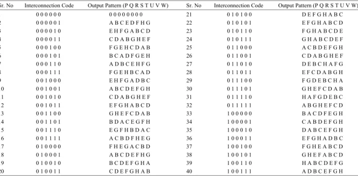
Table 1: Truth Table of the Proposed 8 Input 8Output SPIN (SPIN8X8) with A, B, C, D, E, F, G and H as the inputs
Sr. No Interconnection Code Output Pattern (P Q R S T U V W) Sr. No Interconnection Code Output Pattern (P Q R S T U V W)
1 0 0 0 0 0 0 0 0 0 0 0 0 0 0 21 0 1 0 1 0 0 D E F G H A B C 2 0 0 0 0 0 1 A B C E D F H G 22 0 1 0 1 0 1 E F G H A B C D 3 0 0 0 0 1 0 E H F G A B C D 23 0 1 0 1 1 0 F G H A B C D E 4 0 0 0 0 1 1 C D A B G H E F 24 0 1 0 1 1 1 G H A B C D E F 5 0 0 0 1 0 0 F G E H C D A B 25 0 1 1 0 0 0 A C B D E F G H 6 0 0 0 1 0 1 B C A D F G E H 26 0 1 1 0 0 1 C D A B G H E F 7 0 0 0 1 1 0 A D B C E H F G 27 0 1 1 0 1 0 D E B C H A F G 8 0 0 0 1 1 1 F G E H B C A D 28 0 1 1 0 1 1 E F C D A B G H 9 0 0 1 0 0 0 E H F G A D B C 29 0 1 1 1 0 0 F G D E B C H A 10 0 0 1 0 0 1 A B C D E F G H 30 0 1 1 1 0 1 G H E F C D A B 11 0 0 1 0 1 0 C D A B G H E F 31 0 1 1 1 1 0 H A F G D E B C 12 0 0 1 0 1 1 E F G H A B C D 32 0 1 1 1 1 1 A B G H E F C D 13 0 0 1 1 0 0 G H E F C D A B 33 1 0 0 0 0 0 B A C D F E G H 14 0 0 1 1 0 1 B D A C E G F H 34 1 0 0 0 0 1 C A B D E F G H 15 0 0 1 1 1 0 E G F H B D A C 35 1 0 0 0 1 0 D A B C E F G H 16 0 0 1 1 1 1 A C B D F H E G 36 1 0 0 0 1 1 E F G H A D B C 17 0 1 0 0 0 0 F H E G A C B D 37 1 0 0 1 0 0 F G H E A B C D 18 0 1 0 0 0 1 A B C D E F H G 38 1 0 0 1 0 1 G H E F A B C D 19 0 1 0 0 1 0 B C D E F G H A 39 1 0 0 1 1 0 H A B C D E F G 20 0 1 0 0 1 1 C D E F G H A B 40 1 0 0 1 1 1 A D B C E F G H
An intruder will try various interconnection patterns by be enhanced by increasing the number of bits in the IPC entering different interconnection pattern codes, but bus of the proposed system. For example, if the number of probability of entering correct code is only 1/N where ‘N’ bits in the IPC is selected as 8, total number of possible is the total number of possible interconnection patterns interconnections between inputs and outputs becomes defined for an interconnection network. 2 = 256, which makes the system more resistant against
Truth table of the proposed 8 input 8 output Secured any type of attack.
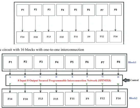
Programmable Interconnection Network (SPIN8X8) is et us consider a simple logic circuit with sixteen shown in Table 1 which is not complete due to space different logic blocks as shown in Fig. 1. Let functionality limitation. There are more than 200 possible of these logic blocks are defined as F1 to F8 acting as interconnection patterns from “ABCDEFGH” to input blocks for blocks F9 to F16 with output of F1 “HGFEDCBA”, but it is limited to 2 where ‘N’ is the widthN connected to F14, output of F2 is connected to F10 etc. of the IPC bus. In the proposed system, N is selected as as shown in Fig. 1. An intruder or trespasser can use the 6, total number of possible output combinations is 2 =64,6 logic system at any time as the system is not secured which means that eight input lines can be shuffled in 64 against various FPGA threat models proposed by various different ways and Table 1 shows only 40 combinations researchers, like copying the bit-stream, modification of out of 64 possible combinations. An attacker who is bit-stream, unauthorized usage of FPGA bit-stream etc. trying all possible combinations of the IPCs, probability Let us enhance the security of the above logic system by of applying the correct code is 1/N, where N=64 for the modifying the design by incorporating 8 input 8 output proposed system. Green coloured cell in Table1 shows the Secured Programmable Interconnection Network correct interconnection pattern with binary value (SPIN8X8). The system under consideration is divided
“001001”. into two parts and they are interconnected using the
The proposed technique can be used to secure a proposed network. The modified diagram is shown in logic circuit, by dividing the digital circuit to be secured Fig. 2.
into two parts and interconnect these two using the By incorporating a SPIN network between various proposed system. An intruder who is trying to use the blocks of the logic circuit, its security can be enhanced as logic system has to apply correct IPC to interconnect shown in the above figure. The blocks are randomly these blocks to form the original circuit. An intruder arranged and input ports of the SPIN8X8 network is cannot find whether he/she had applied the correct defined as ‘A’, ‘B’, ‘C’, ‘D’, ‘E’, ‘F’, ‘G’ and ‘H’ while interconnection pattern code to connect the two blocks to output ports are defined as ‘P’, ‘Q’, ‘R’, ‘S’, ‘T’, ‘U’, ‘V’ reconstruct the original circuit. The level of security can and ‘W’. The truth table of SPIN8X8 is shown in Table 1.
Fig. 1: A logic circuit with 16 blocks with one-to-one interconnection
Fig. 2: Logic circuit divided into two blocks with 8 pair of logic blocks interconnected through the proposed SPIN network
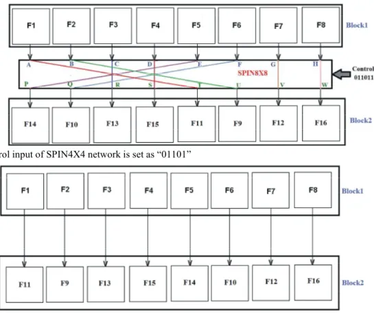
The relationship between inputs and outputs of the SPIN F13 and so on. In this way relationship between input and network depends on the interconnection pattern code or output can be varied by varying the logic value at the “Control” input as shown in Fig. 2. When binary value of “Control” input of the SPIN8X8 network.
the “Control” input is set as “0000000”, all output of the Let us consider a scenario when an intruder trying to SPIN8X8 becomes logic ‘0’, irrespective of the logic use the logic system which should be secure against values at A, B, C, D, E, F, G and H inputs of the SPIN8X8 unauthorized usage. The intruder is not aware of the network. This is highlighted in Table 1 in Red colour. control word to implement a particular function. The A user must apply a binary value other than “000000” as intruder will try various values randomly. Let the binary the interconnection pattern code to establish connection value at the “Control” be “011011”. The SPIN network between various inputs and outputs of the proposed connects A (output of block F1) to T (input of block F11),
system. B (output of block F2) is connected to U (input of
When binary value at the “Control” input is block F9), C (output of block F3) is connected to R “001001”, then P = A, Q = B, R = C, S = D, T = E, U = F, (input of block F13), D (output of block F4) is connected V = G and W = H. In Table 1, this output combination is to S (input of block F15), E (output of F5) is connected to shown in green colour. This means that, when P(input of F14), F is connected to Q, G is connected to V interconnection pattern code or “Control” input is and H is connected to W. Fig. 3 shows the diagram of “001001”, output of F1 is connected to input of F14, various blocks of a system interconnected using SPIN8X8 output of F2 is connected to input of F10, output of block network with “Control” set as “011011”. The resulting F3 is connected to input of F13 and so on as shown in logic function being implemented is shown in Fig. 4. It can Fig. 1. When Control value is changed to “0111111”, be seen that logic values at the output of F1, F2, F5 and output of t he SPIN8X8 network is P = A, Q = B, R=G, S F6 are routed to wrong logic blocks on the other side of = H, T = E, U= F, V= C and W = D. This is shown in Table the SPIN, output of F1 to input of F11, output of F2 to 1 in blue colour. This means that output of block F1 is input of F9, output of F5 to input of F14 and output of F6 applied to input of block F14 through SPIN network, to input of F10. In the actual logic diagram various blocks output of block F2 is F10, output of F7 is connected to are connected as shown in Fig. 1.
Fig. 3: Control input of SPIN4X4 network is set as “01101”
Fig. 4: Actual functionality being implemented when “Control” = “011011”
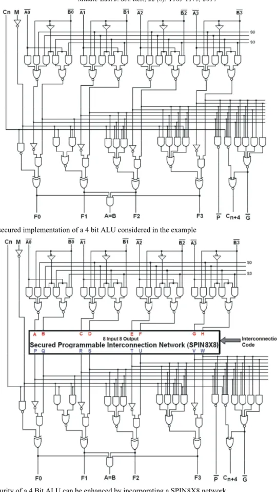
Motivational Example: Let us consider a motivational The interconnections between 8 inputs and 8outputs example to explain the working of proposed system. purely depends only on the binary value at the IPC input For explanation point of view, let us consider a 4 bit ALU, of the system and Table1 shows an incomplete truth table a benchmark circuit to explain “How the proposed system of the SPIN8X8 network which defines the relationship does enhance security against various threat models of a between 8 inputs and 8 outputs for various values of IPC. logic system? Fig. 5 shows the diagram of a 4bit ALU. Relationship between inputs and outputs can be varied This circuit is not secured against any of the threat by varying the binary value of IPC as shown in Table 1. models like copying the bit streams, modifying the Number of possible interconnections between inputs and bit-stream, unauthorized usage of the logic system etc. outputs of the SPIN8X8 network depends on width of the An intruder can easily intrude into the system by IPC input of the SPIN8X8 network. In the proposed applying a set of logic values. The above circuit is not at SPIN8X8 network, width of the IPC is 6 and total number all secure against any of the threat models and is of interconnections defined for the proposed system is vulnerable to any type of attack by an intruder. Level or 64 and probability of applying an interconnection pattern degree of security of the circuit shown above can be is only 1/64. In general, probability of selecting an enhanced by including 8 Input 8 Output Secured interconnection pattern is 1/2 , where N is the width of the Programmable Interconnection Network (SPIN8X8). IPC bus. The degree of security provided by the SPIN Even though the proposed system does not prevent network can be enhanced by increasing the width of IPC modification of bit-stream of the design, it is robust bus. If width of IPC bus is increased by one bit, total enough to prevent two commonly found threat number of possible interconnections gets doubled and models – Bit-stream cloning and unauthorized usage of thus probability of occurrence of an interconnection FPGA based system. The proposed SPIN network acts as pattern by trial and error method can be halved. For an interconnection network between various logic blocks. example, when IPC width is increased from 6 to 7, total Secured version of the 4 bit ALU after incorporating 8 number of possible interconnections becomes 128 and input 8output SPIN network is shown in Fig. 6. probability of application of an IPC becomes 1/128.
Fig. 5: Unsecured implementation of a 4 bit ALU considered in the example
Fig. 6 shows diagram of a modified 4 bit ALU secured A logic system with several numbers of 8-bit buses by incorporating 8 input 8 output Secured Programmable can be made secure by using a system which is the Interconnection Network (SPIN8X8). Eight inputs of the extension of proposed system, which consists of an array SPIN network is defined as A, B, C, D, E, F, G and H, while of SPIN network called SPIN array. SPIN array consists of eight outputs are defined as P, Q, R, S, T, U, V and W. an array of SPIN network, a 6-bit D latch for each SPIN Interconnection between these 8 inputs and 8 outputs of network and an N:2 decoder to generate latch enable the proposed system depends on the Interconnection signals for the latches connected to each SPIN network. pattern Code (IPC) or simply interconnection code. As the The D latch connected to each SPIN network is used to width of the IPC bus is 6 bit, total number of possible hold the interconnection pattern code for that SPIN interconnections between input and output bus are network and as mentioned earlier, interconnection 2 =64. As mentioned previously, Table 1 shows6 between input and output buses of the SPIN network relationship between input bus and output bus of a depends on the interconnection pattern code. SPIN8X8 network which is incomplete and can be Decoder with 2 inputs and 4 outputs generate latch enable expanded up to 64 different input-output relations. (LE) signals for the D flip-flop array as latch. Fig. 8 shows Let us discuss the scenario when an unauthorized the block diagram of a SPIN array with four SPIN person tries to intrude into the system by applying a networks.
random interconnection pattern code to the SPIN8X8 Fig. 8 shows the block diagram of a SPIN array with network. Let the binary value at the IPC input is set as four 8bit-buses and four 8bit output buses which consists “00111”. When interconnection code is set as “001111”, of four SPIN8X8, four 6-bit D latches to hold the the interconnection pattern of the SPIN8X8 network interconnection pattern code for each SPIN8X8 network becomes, P = A, Q = C, R = B, S = D, T = F, U = H, V = E and a 2:4 address decoder which generates LE signals for and W = G. When interconnection pattern code is the four 6-bit D latches. The input and output lines of the “001111” signals at the input side of the SPIN8X8 network SPIN8X8 network are denoted as “I_Bus” and “O_Bus” is routed to wrong logic gates at the output side of the respectively. To re-order the input lines of a SPIN8X8 SPIN8X8 network. Similar is the case when any binary network, first step is to assert the “Ed” input of the SPIN value other than “001001” is applied. If IPC is selected as array as logic ‘1’ to enable the decoder which generates “011111” then the interconnection pattern selected by the LE signal. The interconnection pattern code for a SPIN8X8 network is ABGHEFCD, i.e.; P = A, Q = B, R = G, SPIN8X8 network is placed on the “IPC” input and S = H, T = E, U = F, V = C and W = D. For any IPC other address of the corresponding SPIN network is placed on than “001001”, outputs of logic gates at the input side of the address lines A1 and A0. Based on the binary values the SPIN network is routed to input of wrong logic gates at the address lines A1 and A0, one of the four outputs of and the circuit realized is different from the actual one the address decoder changes which latches the shown in Fig. 5, producing wrong outputs for various interconnection pattern code into the D-latch, defining a input combinations when compared to actual 4 bit ALU. relationship between I_Bus and O_Bus of the SPIN An authentic user will select “001001” as the network connected to that D-latch. Interconnection-interconnection pattern code, for which output of the pattern code is placed on IPC input of the SPIN array and SPIN8X8 network will be P = A, Q = B, R = C, S = D, T = E, decoder is enabled by asserting “Ed” signal as logic ‘1’. U = F, V = G and W = H. For this IPC output of logic The decoder input is set as A1=A0=logic ‘0’which set the blocks in the input side of the SPIN8X8 network is routed latch enable signal of D-latch D0 connected to first to input of actual/right logic gates in the output side of SPIN8X8 marked as S0, loading the interconnection the SPIN8X8 network and thus realizing the actual logic pattern code placed at IPC into that D-latch which defines circuit as shown in Fig. 5 realizing the truth table of a 4 bit interconnection pattern between I_Bus0 and O_Bus0. Let ALU. In short operation of the circuit shown in Fig. 6 can the required interconnection pattern for first SPIN8X8 is be briefed as a logic circuit which realizes a 4 bit ALU I_Bus0(0) = O_Bus0(0), I_bus0(1) = O_Bus0(1), when interconnection pattern code is “001001” and a …...I_Bus0(7) = O_Bus0(7), the binary value required to circuit which behaves in a different manner when IPC is be placed on IPC bus is “001001”. The interconnection different from “001001”. Thus by incorporating the pattern code is placed on the IPC bus and logic values at proposed SPIN network with 8 inputs and 8 outputs, Ed, A1 and A0 are asserted as logic’1’, logic’0’ and security of the logic circuits can be enhanced. Fig. 7(a) logic’0’ respectively. Latch enable signal LE signal of D and Fig. 7(b) shows the behavior of the 4 bit ALU when latch D0 goes high, latching the contents placed on IPC IPC is “001111” and “001001” respectively. bus.
Fig. 7(a): 4bit ALU with SPIN8X8 network with IPC set as “001111”
Fig. 8: Block diagram of a SPIN array which consists of four SPIN networks which can re-order four 8 bit buses
Fig. 9: SPIN array loaded with four different IPC which defines four different interconnection patterns for four SPIN8X8 networks
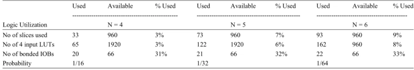
Table 2: Device Utilization Summary for different number of Interconnection Pattern Codes (N)
Used Available % Used Used Available % Used Used Available % Used
--- --- ---Logic Utilization N = 4 N = 5 N = 6 No of slices used 33 960 3% 73 960 7% 93 960 9% No of 4 input LUTs 65 1920 3% 122 1920 6% 162 960 8% No of bonded IOBs 20 66 31% 21 66 32% 22 66 33% Probability 1/16 1/32 1/64
Fig. 9 shows a SPIN array loaded with four different Proposed system, SPIN8X8 with different width of interconnection patterns for the four SPIN8X8 networks. IPC, 4bit, 5bit and 6bit was implemented in VHDL The interconnection pattern code for SPIN8X8 denoted as language using behavioral style of modeling. The number S0 is “001001” which defines the input-output relation as of interconnection patterns is 16 for 4bit IPC, 32 for 5bit P=A, Q=B, R=C, S=D, T=E, U=F, V=G and W=H, where A, IPC and 64 for 6bit IPC. When 4bit IPC was implemented, B, C, D, E, F, G and H are the inputs of a SPIN8X8 network only 3% of total number of slices is utilized. Number of 4 and P, Q, R, S, T, U, V and W are outputs of the SPIN8X8 bit LUTs used is also 3% while 31% of the bonded network. For the SPIN8X8 networks S1, S2 and S3, the Input-Output blocks are used for 8 inputs, 8 outputs and interconnection patterns coders are “001111”, “1001111” 4 bit IPC. For the implementation of a SPIN8X8 with 5 bit and “100100” respectively and input-output relation for wide IPC, which provides 32 (2 ) interconnection patterns, these SPINS are shown in the above figure. Incorporating out of 960 slices only 73 slices are used (7%). Number of a SPIN array in a logic circuit enhances its security as by 4bit LUTs utilized for the implementation of the SPIN8X8 default no interconnection is defined and at runtime an with 32 interconnection patterns is122 (6%) and number authentic user can define the correct interconnection of bonded IOBs is 21 out of 66 (32%). In the case of a pattern by applying appropriate IPC. SPIN8X8 with 6 bit wide IPC bus, 2 or 64 interconnection Experimental Results: The proposed system with 8 input Utilization of 4bit LUTs is just 8% from the 960 available 8 output is modeled in VHDL and behavioral code is 4 bit LUTs. Percentage of utilization of IOBs is almost synthesized using Xilinx ISE 8.1i. SPIN8X8 with same compared to SPIN8X8 with 4 bit wide IPC and 5 bit Interconnection Pattern Codes of different widths was wide IPC. Table 2 shows the device utilization summary implemented and relationship between input and output for different width of IPC. When resource utilization of of the proposed system was verified for different values various SPIN8X8 networks are compared, there is no of IPC. The target device selected was XC3S100E and significant difference between these three networks device utilization summary is shown in Table 2 below. for a particular target device, in this case XC3S100E.
5
6
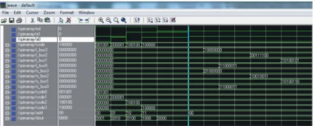
Fig. 10: Simulation result for SPIN array loaded with four different IPC which defines four different interconnection patterns for four SPIN8X8 networks
Probability of application of an interconnection pattern is circuits. Interconnection between input lines and output 1/16, 1/32 and 1/64 respectively. In general, probability of lines of SPIN8X8 depends on the binary value of the application of an interconnection pattern for a SPIN8X8 Interconnection Pattern Code (IPC) of the SPIN8X8 network with ‘N’ bit wide IPC; the probability of network. The default value of the Interconnection Pattern application of an interconnection pattern is 1/N. From Code is “000000” in the case of a 6 bit wide IPC and Table 2, it is evident that, more the number of default output of the SPIN8X8 is defined as logic’0’, i.e., interconnection pattern, less the probability of application all output lines will be at logic’0’ when interconnection of an interconnection pattern and more the degree of code is “000000”. For a SPIN8X8 network as number of
security. possible interconnection between output and input
For big systems with more number of 8bit buses, a depends on the width of the IPC bus, probability of SPIN array was designed and implemented. The proposed application of right interconnection pattern is less for an system consists of four SPIN8X8 networks along with IPC with 6 and more bits. When IPC bus is loaded with a four 6bit D latches and a 2:4 decoder which generates wrong binary value, output of a logic block is routed to a latch enable (LE) signals for the four 6bit latches. There wrong logic block where it is not intended to be. In this are two modes of operation – Program mode and Function way by hiding the routing information or by defining a mode. In program mode all IPCs are loaded into the four D generic routing pattern logic circuits can be made secure. latches and in Function mode signal to be re-ordered are To secure logic systems with multiple buses, a SPIN applied to the four 8bit input buses. Fig.10 shows the array can be used which posses more than one input and simulation results of a SPIN array implemented using output buses. For systems with four 8bit buses, a SPIN VHDL. Left side of the blue line in the following waveform array with four 8-bit input and four 8-bit output buses shows various binary values during Program mode and can be used as explained in the later part of this paper. waveform on the right side of the blue line various values This system enhances the security of the digital system, associated with the SPIN array during Function mode. as an intruder by trial and error method must apply all the During Program mode, four different IPCs are loaded into four IPC codes correctly in a single step. Probability of the D-latches and during Function mode, 8-bit input this is only 1/2 which is almost impossible.
buses are loaded with four different binary values which Compared to logic systems based on cryptography appears re-ordered on the 8-bit output buses. which occupy a large amount of FPGA resources, CONCLUSION not much increment in the complexity and cost of the A Secured Programmable Interconnection Network complex system, due to the above mentioned factors of (SPIN) with 8 inputs and 8 outputs also called as SPIN8X8 cost and complexity. The degree of security can be can be used to amplify the degree of security of digital enhanced by increasing number of possible
24
proposed system provides security ensuring that there is system. Cryptographic systems are less preferred for less
interconnection patterns between input and output of the 9. Goertzel, K.M. and B.A. Hamilton, 2013. Integrated proposed system. For complex systems, security circuits security threats and hardware assurance enhancement can be achieved by using a SPIN array with countermeasures, Crosstalk.
more number of input and output buses. When more 10. Baumgarten, A.C., 2009. Preventing integrated circuit number of SPIN8X8 networks is incorporated, number of piracy using reconfigurable logic barriers”, Master’s input and output buses as well as degree of security of Thesis, Iowa State University, Ames, Iowa.
the system also increases. For example when a SPIN array 11. Ishai, Y., A. Sahai and D. Wagner, 2003. Private with eight 8-bit input and eight 8-bit output buses is used, circuits:securing hardware against probing attacks”, actual width of the interconnection pattern code increases Proceedings of the annual international cryptology to 48 and probability of application of an IPC by trial and conference, California, pp: 463-481.
error method becomes 1/2 , which means better security48 12. Khare, A.A., P.B. Shukla and S.C. Silakari, 2014. compared to a 4 input 4 output SPIN array. Secure and fast chaos based encryption system
REFERENCES Network and Information Security, pp: 25-33. 1. Binu, K. Mathew and K.P. Zacharia, 2014. systems, PhD Thesis, Technical University of
Programmable interconnection network for secured Lisbon, Portugal.
logic circuits, unpublished. 14. Jensen, D.W., D.A. Greve and M.M. Wilding, 1999. 2. Tiri, K. and I. Verbauwhede, 2006. A digital design Secure Reconfigurable Computing, Second Annual flow for secure integrated circuits”, IEEE Trans. on Military and Aero-space Applications of Computer Aided Design of Int. Circuits and Systems, Programmable Devices and Technologies.
25(7): 1197-1208. 15. Valette, N., L. Torres, G. Sassatelli and F. Bancel, 3. Tripathy, A.K., A. Prathiba and V.S. Kanchana 2006. Securing embedded programmable gate arrays Bhaaskaran, 2013. A new improved MCML logic for in secure circuits, 20 Int. Parallel and Distributed DPA resistant circuits, Int. Journal of VLSI Design Processing Symposium.
and Communication Systems, 4(5): 63-75. 16. Zheng, J.X. and M. Potkonjak, 2012. Securing netlist 4. Collins, W.H., 2013. A secure reconfigurable level FPGA design through exploiting process system-on-programmable chip computer system, variation and degradation, Int. conference FPGA’12, Master’s Thesis, University of Tennessee, Knoxville, USA, pp: 129-138.
Tennessee. 17. Rajendran, J., M. Sam, O. Sinanoglu and R. Karri,
5. Zahur, S. and D. Evans, 2013. Circuit structures for 2013. Security analysis of integrated circuit improving efficiency of security and privacy tools”, camouflaging”, Proceedings of the 2013 ACM 34 IEEE symposium on security and privacy, Santh SIGSAC Conference on computer and
Francisco, pp: 1-15. communications security, New York, pp: 709-720.
6. Huffmire, T., B. Brotherton, N. Callegari, J. Valamehr, 18. Costan, V. and S. Devadas, 2011. Security challenges R. Kastner, T. Sherwood and J. White, 2008. and opportunities in adaptive and reconfigurable Designing secure systems on reconfigurable hardware, IEEE Symposium on Hardware Oriented hardware, ACM Trans. On Design Automation of Security and Trust, pp: 1-5.
Electronics Systems, 13(3): 44. 19. Kepa, K., F. Morgan, K. Kosciuszkiewicz and 7. Waksman, A., M. Suozzo and S. Sethumadhavan, T. Surmacz, 2010. SeReCon: A secure reconfigurable 2013. FANCI: Identification of stealthy malicious controller for self-reconfigurable systems”, Int. logic using Boolean functional analysis, Proceedings Journal of Critical Computer Based Systems, of the 2013 ACM SIGSAC Conference on Comp. and 1(1//2/3): 86-103.
Comm. Security, New York, pp: 697-708. 20. Hu, W., J. Oberg, A. Irturk, M. Tiwari, T. Sherwood, 8. Abramovici, M. and P. Bradley, Integrated circuit D. Mu and R. Kastner, 2011. Theoretical security- New threats and solutions, Proceedings of fundamentals of gate level information flow tracking, the 5 Annual Workshop on Cyber Security andth IEEE Trans. on Computer Aided Design of Integrated Information Intelligence Research: Cyber Security Circuits and Systems, 30(8): 1128-1140.
and Information Intelligence Challenges and Strategies, Article No. 55.
using digital logic circuit, Int. Journal of Computer 13. Chaves, R., Secure computing on reconfigurable