http://www.sciencepublishinggroup.com/j/ajop doi: 10.11648/j.ajop.20200801.11
ISSN: 2330-8486 (Print); ISSN: 2330-8494 (Online)
An All Optical Approach to Construct J-K Flip-Flop by
Proper Exploitation of Nonlinear Material
Partha Pratim Das
School of Applied Science & Humanities, Haldia Institute of Technology, ICARE Complex, HIT, Haldia, Purba Medinipur, West Bengal, India
Email address:
To cite this article:
Partha Pratim Das. An All Optical Approach to Construct J-K Flip-Flop by Proper Exploitation of Nonlinear Material. American Journal of Optics and Photonics. Vol. 8, No. 1, 2020, pp. 1-5. doi: 10.11648/j.ajop.20200801.11
Received: August 5, 2019; Accepted: January 18, 2020; Published: January 31, 2020
Abstract:
Optical signal is the best suitable one for data processing and digital signal communication for its inherent parallelism and tremendous operational speed. Conventional electronic or optoelectronic devices are unable to fulfill this due to less speed and time delay. In the case of perfect electronic flip-flop, at the time of switching turned ON, there is noticeable propagation delay on the order of nanoseconds. In the case of an opto-electronic flip-flop, although the propagation delays time is much less than those of a pure electronic flip-flop about 10 to 100 times less, there are many disadvantages still have. Some of these disadvantages are delay of response time due to the use of spatial light modulators, an O/E converter that does not operate at all frequencies or wavelengths, and the unavailability of such materials. An optical input encoding methodology may be the alternative for the performance of two inputs all-optical flip-flop operations. These operations may be conducted in all-optical mode and will be parallel in nature. All the operations may be conducted with proper exploitation of some nonlinear materials. In this communication author reported an optical encoding technique for the construction of clocked J-K flip-flop with two inputs. All the operations are conducted by the proper exploitation of nonlinear materials.Keywords:
Inherent Parallelism, Optoelectronics, Logic Gates, J-K Flip-flop, Optical Nonlinear Material1. Introduction
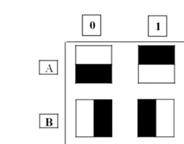
Figure 1. Encoding technique of two binary inputs A and B.
In this communication all the operations have been conducted by the proper exploitation of the inherent parallelism of optical signal and nonlinear material [1, 2]. The spatial encoding and decoding methodology is already accepted for bitwise binary data addition and subtraction [3]. In this process, the inputs become encoded by the combination of presence and absence of light in spatial light
mode. Figure 1 shows the coding technique of two binary variables 0 and 1 for two inputs A and B. By superimposing of two binary inputs A and B, we can get four operations, i.e., AND AB, AB, AB, and NOR, respectively shown in Figures 2(a) – 2(d).
2. Some All-Optical Logic Operations by
Spatial Encoding
The optical imaging system shown in Figure 3 is a lens-based optical technique that makes a complete superimposition of input A with input B in the output screen [4, 5]. The superimposition results come in the form of presence or absence of light in the respective area. Each of four square areas of the output indicates 1 with the presence of optical signal and 0 with the absence of the same.
Figure 3. Four logical operations for the superimposition of two inputs A
and B (NOR,
A
B, AB
, AND).Now let us describe these four logic operations with truth table [10]. When both A an B inputs are 0, we can have the presence of light in the upper-left box in the output screen. Hence, we get all outputs of these four operations to be 0 except NOR output, which is 1.
When input A is 0 and B is 1, we get the presence of light in the upper-right box of the output screen. Hence, we get all outputs of these four operations to be 0 except
A
B output, which is 1.When input A is 1 and B is 0, we get the presence of light in the lower-left box of the output screen. Hence, we get all outputs of these four operations to be 0 except A
B
output, which is 1.When both A and B inputs are 1, we get the presence of light in the lower right box of the output screen. Hence, we get all outputs of these four operations to be 0 except AND output, which is 1.
Table 1. Truth table for AND, A
B
,A
B and NOR Operation.Input(s) Output(s)
A B AND AB AB NOR
0 0 0 0 0 1
0 1 0 0 1 0
1 0 0 1 0 0
1 1 1 0 0 0
3. Use of Nonlinear Material for Some
Other Logic Operation
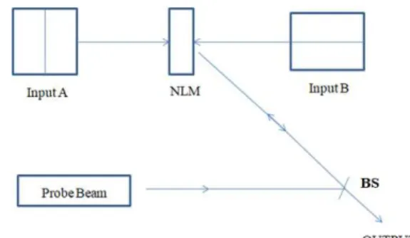
Optical nonlinear material (OPNLM) used here successfully to get different logical operations [10]. Potassium dyhydrogen phosphate, simply known as KDP crystal (KH2PO4) or lithium niobate (LiNbO3) of considerable size may be used successfully as a switching
device for this purpose [6, 7]. In Figure 4, the operational technique of OPNLM as switching device is shown. The reflected probe beam from the OPNLM gives the output. If the two read beams from two opposite sides of the OPNLM are given in a spatially encoded form and the two forms of the beams are superimposed completely on the OPNLM, then the probe beam will be reflected back only from that position of OPNLM where two read beams present and no light will come back from the other positions of the same.
Figure 4. Operational technique of an optical nonlinear material (OPNLM).
Figure 5. Optical implementation of four logical operations for the superposition of two inputs A and B, i.e., AND, A
B
,A
B and NOR by optical nonlinear material (OPNLM).When both A and B inputs are high, only position 1 of Figure 5 gets light from both input read beams. Hence, the NLM of position 1 is active, and the probe beam falling on this position will be reflected back and comes as an NOR output. In this case, other positions 2, 3, and 4 of the NLM are inactive, as they are not excited by the input read beams from both sides, and hence we get no light for
A
B, AND,and A
B
outputs, which are treated as 0.of NLM, giving the case of
A
B operation, and other probe beams from positions 1, 3, and 4 of the NLM will not be reflected, givingA
B output as 1 and other outputs as 0.Similarly, position 4 of the NLM will receive two light beams from two opposite sides when A is 0 and B is also 0. So the probe is reflected back only from position 4 of the NLM, giving the case
of AND operation, and other probe beams from positions 1, 2, and 3 of the NLM will not be reflected, giving AND output as 1 and other outputs as 0.
4. Optical Flip-Flop with Nonlinear
Material
Here, by proper exploitation of nonlinear material I have designed an all-optical J-K flip-flop using nonlinear material [8, 9]. The coding techniques for inputs J and K are given in Figure 6. Input J takes the value 1 i.e., high input value when the upper rectangular half is opaque and the lower rectangular half is transparent. In this way, when the upper rectangular half is transparent and the lower rectangular half is opaque, it takes the value 0 i.e., low input value. Similarly, input K takes the value 1 i.e., high input value when the right rectangular half is transparent and the left rectangular half is opaque. In this way, when the left rectangular half is transparent and right rectangular half is opaque, it takes the value 0 i.e., low input value. The +ve spatial light modulator SLM has the character of allowing a light beam to pass through it if it has sufficient optical triggering signal and is opaque if there is no optical triggering signal. Similarly, -ve
SLM has the character of allowing a light beam to pass through it if it has no optical triggering signal and is opaque if there is sufficient amount of optical triggering signal. By the use of an SLM-based input coded system and also by the use of different optical component like beam splitters (BSs), mirrors (Ms), etc., the all-optical scheme of developing a J-K flip-flop, which is shown in Figure 7 proposed here. The optical nonlinear material OPNLM is used very successfully to get flip-flop functioning.
Figure 6. Coding of two binary variables K and J.
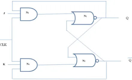
Figure 7 shows the basic block diagram of a clocked J-K flip-flop. Between two clock pulses at clock= 0 stage, the outputs of N3 and N4 are 1 independent of the values of J and K, i.e., the flip-flop does not change the state between clock pulses, it is invariant within a bit time given in Table 2. When a clock is present at clock= 1 stage, the truth table follows Table 2. When J = 0 and K = 0 at clock= 1, it shows the previous state as electronic J-K flip-flop. When J = 1 and K = 1 clock= 1, it remains intact and shows the previous state of J = 0 and K = 1 clock= 1. When J = 1 and K = 0 at clock = 1, output changes its state only.
Figure 7. Conventional clocked electronic J-K flip-flop.
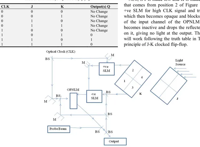
We have used here the OPNLM only for the beam from position 1 of the superimposed beams of J and K structures, as given in Figure 8. The clock CLK signal optical is driving one end of the OPNLM material and a +ve SLM that is controlling the light emerging from position 2 of Figure 8 for J = 0 and K = 1. This light passing through the +ve SLM only for high CLK values, and again it triggers a-ve SLM introduced in the path of the light beam coming from position 3 of Figure 8.
Table 2. Truth table for optical J-K flip-flop.
CLK J K Output(s) Q
0 0 0 No Change
0 0 1 No Change
0 1 0 No Change
0 1 1 No Change
1 0 0 No Change
1 0 1 0
1 1 0 1
1 1 1 0
Now, if J is made low and K is made high, the light beam that comes from position 2 of Figure 8 passes through the +ve SLM for high CLK signal and triggers the -ve SLM, which then becomes opaque and blocks the light on one side of the input channel of the OPNLM. The OPNLM then becomes inactive and drops the reflected probe beam falling on it, giving no light at the output. The system in Figure 8 will work following the truth table in Table 2 to support the principle of J-K clocked flip-flop.
Figure 8. Clocked J-K flip-flop using OPNLM.
For other values of J and K, the output does not change i.e., the earlier values remain intact, as given in the truth table. Here, the high and low values of the output are given by the presence or absence of light, respectively. Thus, we have designed a clocked J-K flip-flop, avoiding the race around condition.
Here, I use a continuous He-Ne laser as the probe beam, with power about 2 mW and wavelength 6.328310−5 cm.
5. Conclusion
This methodology used in the spatial input encoding is not only an all-optical method for conducting logical and flip-flop memory operations, but it is also a method of parallel handling of optical signals. Here, the number of logic operations are four for both the cases of optical imaging device based systems as well as nonlinear material based systems. This spatial input encoding technique for an all-optical logical operation can be extended for three or higher input logic systems also. This technique will give better responses with the suitable and better availability of NLM. It should be mentioned that diffraction is a major limitation. The diffraction will restrict the selection of input-output cell dimensions, and we should be very cautious about the diffraction limitation in the image processing technique. The scheme in Figure 8 will be possible to be operated systematically if suitable optically driven NLM be found. However, the J-K flip-flop is different from its electronic
counterpart when CLK= 1, J = 0, and K = 0. Here, we get a no concrete output i.e., its value is continuous here, when clock is 0. As it is an all-optical system, we may get the flip-flop with real-time operations.
References
[1] R. P. Bocker, B. L. Drake, M. E. Lasher, and T. B. Henderson, “Modified signed-digit addition and subtraction using optical sym-bolic substitution,” Appl. Opt. 25, 2456–2457 1986.
[2] B. L. Drake, R. P. Bocker, M. E. Lasher, R. H. Patterson, and W. J. Maceli, “Photonic computing using the modified signed-digit number representation,” Opt. Eng. 25, 38–43 1986.
[3] S. Mukhopadhyay, “Binary optical data subtraction by using a ter-nary digit representation technique in optical arithmetic problems,” Appl. Opt. 31, 4622–4623 1992.
[4] B. Liu, L. Liu, L. Shao, and H. Chen, “Matrix–vector multiplication in a photorefractive crystal,” Opt. Commun. 146, 34–38 1998.
[5] C. Denz, T. Dellwig, J. Lembeke, and T. Tschudi, “Parallel optical image addition and subtraction in a dynamic photo-refractive memory by phase code multiplexing,” Opt. Lett. 21, 278–283 1996.
[7] A. Basuray, S. Mukhopadhyay, H. K. Ghosh, and A. K. Datta, “A tristate optical logic system,” Opt. Commun. 85, 167–170 1991.
[8] T. Kacprzak, “Analysis of oscillatory metastable operation of an RS flip-flop,” IEEE J. Solid-State Circuits 23 (1), 260–266 1988.
[9] D. Samanta and S. Mukhopadhyay, “Implementation of an optical S-R flip-flop with polarization encoded light signals,” Optoelectron. Lett. 5 (1), 57–60 2009.
[10] D. Giri and P. P. Das, New alternative approach to all-optical flip-flop with nonlinear material,” Optical Engg. 49 (7), 075201 (1-5), 2010.