NCP1351 Modeling Using
the PWM Switch Technique
Prepared by: Stéphanie Conseil
ON Semiconductor
This document describes the average modeling of the NCP1351 a fixed on time / variable off time controller. The advantage of using an average model is that you can perform ac simulations of your power supply to study the stability of your system. Another advantage is that transient simulations with the averaged model are faster compared to transient simulations with a cycle−by−cycle model. The model is very simple to use and can be downloaded from ON website.
Presentation of the PWM Switch Technique
The Pulse Width Modulation switch model was developed by Vatché Vorpérian (Jet Propulsory Laboratory, Passadena, CA) in 1986. His approach consisted in modeling the switch network alone (power switch + diode)
by averaging the voltage and current waveform in the circuitry.
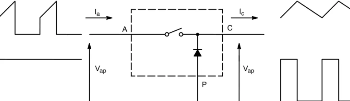
He obtained a 3 terminal model (node A, C and P) where:
•
Node A represents the active node, the switch terminal not connected to the diode•
Node C is the common node, the junction between the power switch and the diode•
Node P is the passive node, the diode terminal not connected to the switchThe input variables are the current in node A, the voltage Vap; the output variables are the current in node C and the
voltage Vap (Figure 1).
Figure 1. PWM Switch and its Variables P
Vap
Ic
Vap
C Ia
A
The PWM switch is invariant i.e. the PWM switch electrical structure is the same whatever converter we consider. For this reason, we will use a buck−boost converter for the study, because of simplicity but also because the flyback topology where the NCP1351 is used is derived from buck−boost.
Modeling the Switching Network
Figures 2 and 3 show the switching network in the buck−boost circuit and its equivalent implementation in PWM switch.
Figure 2. Buck−Boost Converter R C +
Vin
SW
PWM
L1 D
APPLICATION NOTE
http://onsemi.comFigure 3. PWM Switch in the Buck−boost Converter +
L1 33 m
C1 220 m
Rload
6 X1
PWMVM
PWM
Vin
18
PWM Switch VM
a d
c p
4 3
2
1
Once the switch network has been identified in the original circuit, a simple rotation of the PWM switch model leads to the final implementation. This step is necessary to unveil the various variables in play.
Averaging the PWM Switch Waveforms
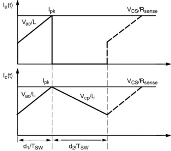
NCP1351 is a fixed peak−current variable−toff current−
mode converter without internal ramp compensation. We will first consider the DCM mode to derive the equations since further developments will show that the model automatically toggles from DCM to CCM. The method consists of identifying current, voltage waveforms in the switch terminals (Figure 4 and Figure 5) and averaging them over one switching period.
Figure 4. The Current Waveforms in DCM: Ia, Ic Figure 5. The Current Waveforms in CCM: Ia, Ic Ipk
Vac/L
VCS/Rsense
VCS/Rsense
Ia(t)
Ic(t) I pk
Vac/L Vcp/L
d2/TSW
d1/TSW d3/TSW d1/TSW d2/TSW
VCS/Rsense
VCS/Rsense
Ia(t)
Ic(t)
Ipk
Vac/L
Vac/L
Ipk
Vcp/L
The average current flowing in the C terminal is given by the following equation [1]:
IC+RsenseVCS *d2TSWVCPL
ǒ
1*d1)2 d2Ǔ
(eq. 1)According to Figure 4, the following expressions for the terminal voltages and currents can be easily verified [2]:
Vac+L IPK
d1TSW (eq. 2)
Vcp+L IPK
d2TSW (eq. 3)
Ia+IPK2 d1 (eq. 4)
Ic+IPK2 (d1)d2) (eq. 5)
The average current in terminal A is deduced from equations (4) and (5):
Ia+Ic d1d1)d2 (eq. 6)
The average on−time duty cycle d1 is solved from
Equations (2) and (3)
It is necessary to clamp the duty cycle d1 value between 0.01
and 0.9 (1 to 90% duty−cycle) to avoid convergence issues.
d1+d2VcpVac (eq. 7)
d2 expression is derived from Equations (2) and (5)
d2+d1TSWVac2LIc *d1 (eq. 8)
We clamp d2 value between 0.01 and (1– d1). When d2 is
equal to (1– d1), we are in CCM [1].
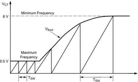
In the NCP1351, the loop controls the switching frequency by adjusting the end−of−charge voltage threshold of the Ct capacitor (see Figure 6). The capacitor is charged
by a constant current source ICt and the threshold voltage
Vfbint is proportional to the feedback current injected into
the FB pin by the optocoupler. The switching period equation is:
Figure 6. The Switching Frequency is Controlled by the Charge of Ct Capacitor TSW
Vfbint
TSW
Maximum Frequency
Minimum Frequency
0.5 V 6 V VCT
NCP1351 is a current mode converter without ramp compensation. The controller is thus subject to subharmonic oscillations when operating in CCM. The subharmonic oscillations are modelled by a capacitor connected between C and P terminal during CCM. The capacitor value is frequency−dependent and is calculated by the following expression [3]:
CS+L(pFSW)4 2 (eq. 10)
A separate in−line equation disconnects the capacitor during DCM. The electrical implementation of all the equations derived above is shown on Figure 7.
Modeling the FB Section
To avoid acoustic noise problems, the NCP1351 compresses the peak current as the load becomes lighter. From the datasheet, we can extract the values of CS current as a function of FB current.
250mA if Ifbt60mA
(eq. 11)
70mA if Ifbu80mA
790mA*9 Ifb if 60mAtIfbt80mA
ICS+
A behavioral current source is used to model ICS. The
model for the peak current compression is shown on Figure 8.
The feedback current controls the switching frequency by changing the timing capacitor end−of–charge−voltage
Vfbint. To do so, the optocoupler injects current into the FB
pin which is actually a bipolar current−mirror input. This current is then adjusted by the feedback loop depending on the operating region (full power, compression or standby). The resulting current flows into a 45 kW resistor which develops a voltage proportional to the FB current. This signal becomes the Ct capacitor ending voltage.
Thus, the relation between feedback current Ifb and Vfbint
is:
Vfbint+Voffset)45 kIFB (eq. 12)
It is also important to model the pin FB current mirror because the dynamic resistance of the input mirror transistor directly influences the loop gain. Figure 7 shows the way we implemented the model of the FB modulator.
Figure 7. Feedback Modulator Model
VFBint FB
+ +
+
B1 Current C4
80 p R1
45 k D2
1N4148
Vcl_Vfb 6 Voffset
0.5
X5 NPNV
Vlfb 0 9 1
2 l(Vlfb) < 42 m
0.4 m: l(Vlfb) − 41.1 m
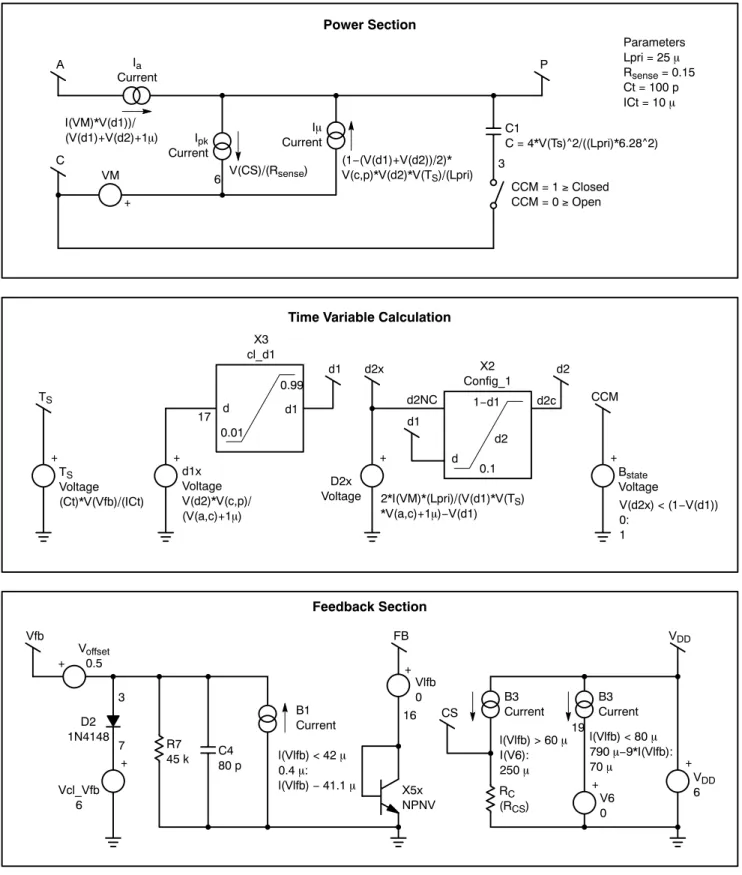
Complete Average Model and Application
The complete averaged model of NCP1351 is shown below.
Figure 8. Complete Averaged Model of NCP1351 Feedback Section
Time Variable Calculation Power Section
+
+ +
Vfb
+
X5x NPNV
Vlfb 0 16 l(Vlfb) < 42 m
0.4 m: l(Vlfb) − 41.1 m
FB
B1 Current C4
80 p R7
45 k D2
1N4148
Vcl_Vfb 6
VDD
+ B3
Current B3Current
RC
(RCS) V60
VDD
6 CS
l(Vlfb) > 60 m
I(V6): 250 m
l(Vlfb) < 80 m
790 m−9*I(Vlfb): 70 m
+ C
A P
VM Ia
Current
CCM = 1 ≥ Closed CCM = 0 ≥ Open C1
C = 4*V(Ts)^2/((Lpri)*6.28^2) Ipk
Current
V(CS)/(Rsense)
Im
Current
(1−(V(d1)+V(d2))/2)* V(c,p)*V(d2)*V(TS)/(Lpri)
6
3
Parameters Lpri = 25 m
Rsense = 0.15
Ct = 100 p ICt = 10 m
+ CCM
Bstate
Voltage +
TS
TS
Voltage (Ct)*V(Vfb)/(ICt)
+
d1
+
d2 d2x
d1
D2x Voltage X3
cl_d1
X2 Config_1 17
d1x Voltage V(d2)*V(c,p)/ (V(a,c)+1m)
2*I(VM)*(Lpri)/(V(d1)*V(TS)
*V(a,c)+1m)−V(d1) V(d2x) < (1−V(d1))0: 1
Voffset
0.5 I(VM)*V(d1))/ (V(d1)+V(d2)+1m)
d
0.99 0.01
d1 d2NC d2c
d 0.1
d2 1−d1
19 3
All the elements in Figure 8 are encapsulated into a subcircuit as shown below:
Figure 9. The PWM Switch Encapsulated into a Sub Circuit 7 6 3 2 P C A FB CS 1 4 5
TS CCM
X1
NCP1351_av Lpri = 33 m
Rsense = 0.27
RCS = 3.9 k
CT = 100 p
PWM Switch CCM−DCM
•
A, C and P are the power terminals.•
FB is the feedback input. Connect it to optocoupler emitter.•
The CCM pin indicates the operating mode (CCM or DCM):1. if equal to “1”, the converter is in CCM 2. if equal to “0”, the converter is in DCM
•
Ts and CS respectively indicate the switching period (1mV = 1 ms) and the CS level. Place voltage probes on the schematic to see their values or display theoperation bias points
The model expect the values of your primary inductance, sense and CS resistors and the value of the timing capacitor
Ct. Defaults values for these parameters are indicated on
Figure 9.
The Model in a Flyback Converter
The following schematic describes the NCP1351 averaged model implementation in a flyback converter. This schematic can be downloaded from the website. Then, you will just need to enter your own power supply design values in the different components.
Figure 10. The NCP1351 Model in a Flyback Converter 7
6 3
2 P
C A FB CS 1
TS
CCM
X5 PWMCMTS Lpri = 650 m
Rsense = 0.9
RCS = 3.9 k
CT = 270 p
L2 (Lpri) Rupper 38 k Rbias 560 Rfb 1 k Rlower 10 k CZ 100 n Vin
Vout Vac
AC = 1 + + X2 TL431_G 11 10 9 Rp
2.5 k 100 nCP Vout
FB
X1 Optocoupler Cpole = 6.8 n
CTR = 0.768 V3 18 13 VCS FB + R11 0.09 Rload 6 R2 0.033 L1 0.5 m
X4 XFMR RATIO = −0.125
C4 100 m
Cout
1880 m
IC = 12
21 8 PWM Switch CCM−DCM VIN 125 AC = 0
25
12
As an example we implemented a 12 V, 2 A flyback converter with secondary output filter. For the feedback, we have chosen a TL431, but you can also use a zener diode. Rp
is the optocoupler pulldown resistor and Cp places a pole in
the compensation transfer function. Typical values for these components are shown on the schematic. We have also represented the ESR of output capacitors to be closer to real application and also because it influences the ac response of the power stage.
Validating the Model: Model versus Reality
In order to test the model, we built a 20 W buck−boost converter with NCP1351 as the MOSFET controller. The design specifications are:
Input voltage: 16 V – 20 V dc Output voltage: 12 V @ 1.7 A
As we used a P−channel MOSFET for the power switch, the DRV signal from NCP1351 needs to be inverted. We selected a MC33151 for that purpose. The output power is regulated with a zener diode and an optocoupler. The optocoupler simplifies the FB path as we need to pull the FB up from a negative output voltage.
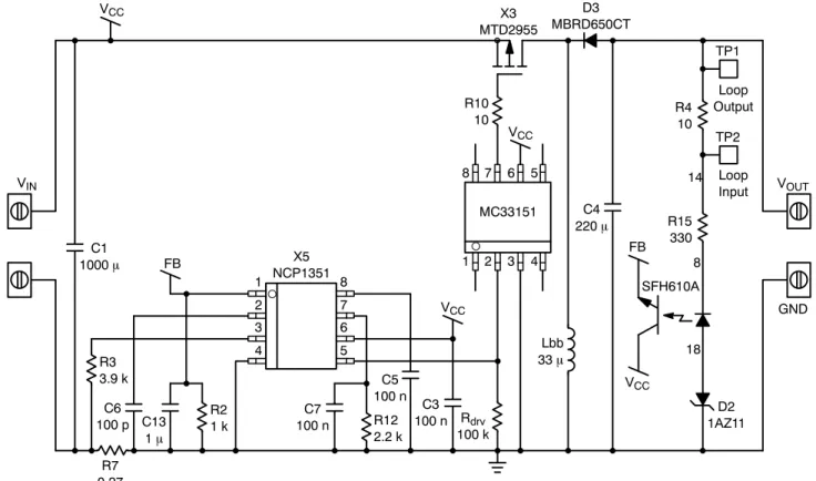
Figure 11. The Buck−boost Board Application Schematic Shows an Optocoupler in the FB Chain
Figure 12. The Buck−boost Model Implemented in SPICE 7
6 3
1 P
C A FB CS 2 TS CCM L2 (Lpri) VCS + PWM Switch CCM−DCM VIN 18.33 Cin
1000 m
R1 75 m Rload 8.7 + V2 IP R2 0.15 Cout
220 m
IC = −12
Vout
Rfb
340 Vin
Vout Vac
AC = 1 + D1 1AZ11 10 4 R8 88 m X1 Optocoupler Cpole = 6.8 n
CTR = 0.768
7 FB
VCC
Parameters RCS = 3.9 k
Lpri = 33 m
Rsense = 0.27
FB VCC
X3
NCP1351_av
Cp 1 m
Rp 1 k 23 R2 1 k R3 3.9 k C6 100 p C13
1 m
C1
1000 m FB VCC VCC C7 100 n C5 100 n R12 2.2 k C3 100 n Rdrv
100 k VCC 18 8 14 VCC FB Lbb 33 m
C4 220 m
Loop Input Loop Output TP1 TP2 R4 10 R15 330 D2 1AZ11 R10 10 MC33151 X5 NCP1351 VOUT GND VIN 1 2 3 4 8 7 6 5
1 2 3 4 8 7 6 5
R7 0.27 SFH610A X3 MTD2955 D3 MBRD650CT 12 4
As we said in the previous section, it is important to include the dc resistance of the self and the ESR of the capacitors in the model to better fit reality.
Operating Point
We ran operating point simulations for different loads. We obtain the following results for the switching period:
Load Current – Iload Simulated Period – Tsw Measured Period – Tsw
1.4 A 11.7 ms 13.7 ms
0.6 A 17 ms 17.4 ms
0.09 A 22.3 ms 21 ms
In high current conditions, the forward drop voltage in the diode and the ohmic losses in the MOSFET can degrade the bias point as these effects are not taken into account in our model. However, at a low output current, these losses become negligible and the simulation better fits the measurement.
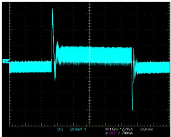
Load Step Response
We compared the simulated and the measured response for a load step from 0.5 A to 1.4 A swept with a slew−rate of 10 mA/ms (Figure 13 and Figure 14).
Figure 13. Simulated Load Step Response Figure 14. Measured Load Step Response Scale : Y = 20 mV / div, X = 1 ms / div Scale : Y = 20 mV / div, X = 1 ms / div
Vout
The simulated results are very close to measurements. The first voltage peak corresponding to a transition from 0.5 A to 1.4 A is well predicted with a simulated value of 80 mV versus 70 mV for the measurement. For a transition from 1.4 A to 0.5 A, the model is less precise and the simulation response is 40 mV higher than the measurement. This may come from the internal Cs capacitor that is brutally
disconnected between C and P terminal since we are
toggling from CCM to DCM. A solution would be to disconnect this capacitor for transient simulations only.
Measuring the Loop Response
The loop measurement represents an important task to confirm the validity of the assumptions during the theoretical design stage. The measurement principle is shown below:
Figure 15. Loop Response Measurement Principle Power Stage
Controller NCP1351
Rload
VOUT
Network Analyzer Isolator
R4 10 R15 330 SFH610A
VCC
D2 1AZ11
TP1
TP2 Loop Input Loop Output
The voltage injection source is implemented with a wide band isolation device together with a 10 ohm resistor. See reference [4] for more information about this technique. Voltage probes are used to measure the loop input and output signals with respect to ground on either side of the injection point.
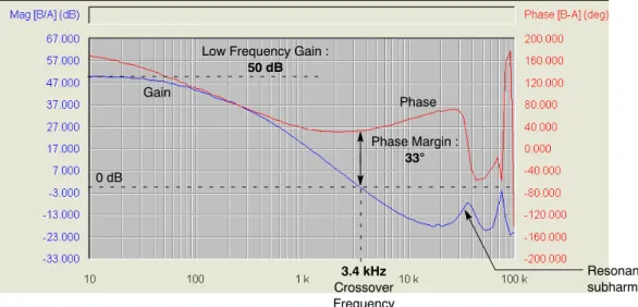
Results in CCM
To obtain correct measurements, it is necessary to choose an operating point outside the peak current compression zone. We have selected Vin = 18 V and a output current of
1.4 A. The switching frequency is 73 kHz. The below figures represent the measured and simulated loop gain and phase for a 1.4 A output current.
Phase Gain
Phase Margin : 335
3.4 kHz Crossover Frequency 0 dB
Low Frequency Gain : 50 dB
Resonance due to subharmonic oscillations Figure 16. Measured Loop Response in CCM
Figure 17. Simulated Loop Response in CCM 1 phase 2 gain
10 100 1k 10k 100k
frequency in hertz −23.0
−3.00 17.0 37.0 57.0
gain
in db(volts)
−160 −80.0 0 80.0 160
phase
in degrees
Plot1
1 2 Gain
Low Frequency Gain : 45 dB
Phase 0 dB
Resonance due to subharmonic oscillations Phase
Margin : 375
3.9 kHz Crossover Frequency
The simulated loop response is very close to reality. We have a variation of 10% between measurement and reality, which is acceptable because what we need is an indication about phase margin (greater than 455) and crossover frequency to be sure we will remain stable in all operating cases. In our example, we have a phase margin smaller than 455. This is clearly not acceptable as a design goal but as our
primary aim was to validate the model, we did not pay a particular attention to improve this figure.
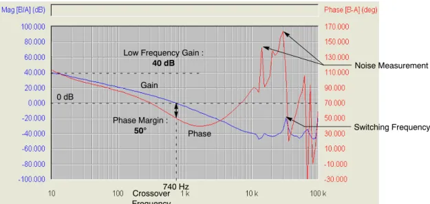
Results in DCM
We also compared the simulated and measured loop response in DCM for a 0.06 A output current. The input voltage is 18 V and the switching frequency is 33 kHz (Figure 18 and Figure 19).
Phase Margin : 505
Crossover Frequency 0 dB
Low Frequency Gain : 40 dB
740 Hz
Switching Frequency Noise Measurement Gain
Phase
Figure 18. Measured Loop Response in CCM
10 100 1k 10k 100k
−80.0
−40.0 0 40.0 80.0
gain_dcm
in db(volts)
−10.0 30.0 70.0 110 150
phase_dcm
in degrees
Plot1
Crossover Frequency Phase Margin
505
0 dB
Figure 19. Measured Loop Response in DCM Phase
Gain
FREQUENCY (Hz) 723 Hz
Low frequency Gain 39 dB
Again, we have a good correlation between measured and simulated loop response in DCM. The error ratio between simulation and measurement is less than 2%, the model is thus accurate to predict the DCM behavior. Here, we have a greater phase margin because the right half plane zero in the control to output transfer function of the buck−boost disappears, thus improving the system stability.
Conclusion
An averaged model of NCP1351 has been derived using the PWM Switch modeling technique.
The model has been validated by experimental measurements on a buck−boost converter using NCP1351 as the controller. Several aspects of the model have been tested
and compared to measurements: operating point, load step, and loop gain and phase response. There is a good correlation between the model and the measurements. We can conclude that the model is a good tool to predict the small−signal response of a NCP1351−based power supply. This model has been derived using INTUSOFT’s IsSpice and CADENCE’s OrCAD. Both versions are uploaded on ON Semiconductor website (www.onsemi.com). A cycle−by−cycle model also exists and is available from the same location.
References
1. Christophe Basso, “The PWM Switch concept included in mode transitioning SPICE models”, PCIM 2005
2. Vatché Vorpérian, “Simplified Analysis of PWM converters using the model of the PWM switch, Part I (CCM) and II (DCM)”, Transactions on
Aerospace and Electronics Systems, Vol 26, N°3, May 1990.
3. Vatché Vorpérian, “Analysis of current−mode controlled PWM converters using the model of the current−controlled PWM switch”, Power
Conversion October 1990 proceedings. 4. www.ridleyengineering.com
ON Semiconductor and are registered trademarks of Semiconductor Components Industries, LLC (SCILLC). SCILLC reserves the right to make changes without further notice to any products herein. SCILLC makes no warranty, representation or guarantee regarding the suitability of its products for any particular purpose, nor does SCILLC assume any liability arising out of the application or use of any product or circuit, and specifically disclaims any and all liability, including without limitation special, consequential or incidental damages. “Typical” parameters which may be provided in SCILLC data sheets and/or specifications can and do vary in different applications and actual performance may vary over time. All operating parameters, including “Typicals” must be validated for each customer application by customer’s technical experts. SCILLC does not convey any license under its patent rights nor the rights of others. SCILLC products are not designed, intended, or authorized for use as components in systems intended for surgical implant into the body, or other applications intended to support or sustain life, or for any other application in which the failure of the SCILLC product could create a situation where personal injury or death may occur. Should Buyer purchase or use SCILLC products for any such unintended or unauthorized application, Buyer shall indemnify and hold SCILLC and its officers, employees, subsidiaries, affiliates, and distributors harmless against all claims, costs, damages, and expenses, and reasonable attorney fees arising out of, directly or indirectly, any claim of personal injury or death associated with such unintended or unauthorized use, even if such claim alleges that SCILLC was negligent regarding the design or manufacture of the part. SCILLC is an Equal Opportunity/Affirmative Action Employer. This literature is subject to all applicable copyright laws and is not for resale in any manner.
PUBLICATION ORDERING INFORMATION
N. American Technical Support: 800−282−9855 Toll Free
USA/Canada
Europe, Middle East and Africa Technical Support: LITERATURE FULFILLMENT:
Literature Distribution Center for ON Semiconductor P.O. Box 5163, Denver, Colorado 80217 USA
ON Semiconductor Website: www.onsemi.com Order Literature: http://www.onsemi.com/orderlit