e-ISSN: 2278-067X, p-ISSN: 2278-800X, www.ijerd.com
Volume 12, Issue 8 (August 2016), PP. 66-71
High Speed Area Efficient 2×2 And 3×3 Fast Parallel FIR Filter
Using Kogge-Stone Adder
Richa Chauhan
1, M. Zahid Alam
2Dept. of Electronics and Communication Engineering LNCT, Bhopal
Abstract:
In the advanced digital technology the need is of high speed in real time system along with the improvement in implementation issue. Vedic Multipliers has been used to solve the typical and tedious engineering calculation by simple Vedic methods. Here in this paper we have proposed 2x2 and 3x3 parallel FIR filter with kogge stone adders replacing the traditional carry select adder The Vedic multiplier has also been designed using this Kogge-stone adder to improve the propagation delay time and area on silicon chip. With this slight improve in the multiplier, great results have been achieved in signal processing tasks. The VM has been designed for the target device XC3S400 -5 PQ208.I.
INTRODUCTION
Due to the explosive growth of multimedia application, the demand for high-performance and low-power digital signal processing (DSP) is getting higher and higher. Finite-impulse response (FIR) digital filters are one of the most widely used fundamental devices performed in DSP systems, ranging from wireless communications to video and image processing. Some applications need the FIR filter to operate at high frequencies such as video processing, whereas some other applications request high throughput with a low-power circuit such as multiple-input multiple-output (MIMO) systems used in cellular wireless communication. Furthermore, when narrow transition-band characteristics are required, the much higher order in the FIR filter is unavoidable. For example, a 576-tap digital filter is used in a video ghost canceller for broadcast television, which reduces the effect of multipath signal echoes. On the other hand, parallel and pipelining processing are two techniques used in DSP applications, which can both be exploited to reduce the power consumption. Pipelining shortens the critical path by interleaving pipelining latches along the data path, at the price of increasing the number of latches and the system latency, whereas parallel processing increase the sampling rate by replicating hardware so that multiple inputs can be processed in parallel and multiple outputs are generated at the same time, at the expense of increased area. Both techniques can reduce the power consumption by lowering the supply voltage, where the sampling speed does not increase. In this paper, parallel processing in the digital FIR filter will be discussed.
The paper is organized as follows: Section II proposes the related work. Section III contains architecture of proposed Vedic multiplier using carry Boolean logic Section IV provides proposed methodology for Vedic multiplier. Section V contains results and discussion. Section VI conclusions followed by future work.
II. RELATED WORK
In general, two parallel FIR filter can be expressed as
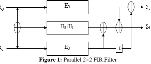
Traditional two parallel digital FIRS filter is shown in figure 1. For this two parallel FIR filter L=2. This will require three FIR sub-filter blocks of length N/2, one pre-processing adder and three post-processing adders. Total number of multiplier and adders required are 3N/2 and 3(N/2-1) + 4 respectively.
Figure 1: Parallel 2×2 FIR Filter
Figure 2: Proposed Parallel 2×2 FIR Filter
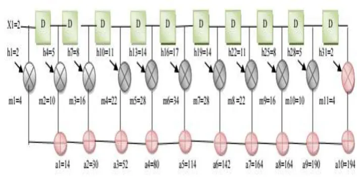
This same process is used for the n number of bits and thus we get the final sum and carry as output. Example 1: Consider a 33-tap FIR filter with a set of symmetric coefficient as follows:
{h(0), h(1), h(2), h(3), h(4),…………...h(29), h(30), h(31)}
Where h(0) = h(32), h(1) = h(31), h(2) = h(29), h(3) = h(28)
h(12) = h(20)
Figure 3: Internal Structure of H1
The symmetric parallel FIR filter is shown in Figure 2. The three parallel FIR filter consists of filter blocks. The input to the system is represented as A0, A1 and the response of the system as Z0 and Z1. Let X0=5, X1= 2, X2=3. The filter blocks H1 with its mod 3 coefficients are shown in Figure 3.
The proposed high speed Vedic multiplier is used in parallel FIR architecture. The proposed technique improves the speed of FIR filters and area utilization when compared to traditional Vedic multiplier.
Figure 4: Three parallel FIR filter implementation using FFA
)])}
)(
(
)
)(
[(
2
/
1
)
)(
((
)
)(
{(
2 0 2 0 2 0 2 0 0 0 2 0 2 0 1 1 2 1 2 1 3 0 0 0A
A
F
F
A
A
F
F
A
F
A
A
F
F
X
F
A
A
F
F
z
A
F
Z
} )] )( ( ) )( [( 2 / 1 ) )( {( } )] )( ( ) )( [( 2 / 1 ) )( {( ) )( ( ) )( ( ) )( ( 0 0 2 0 2 0 2 0 2 0 2 0 2 0 3 0 0 2 0 2 0 2 0 2 0 2 0 2 0 2 0 2 0 2 1 2 1 3 2 0 2 1 0 1 A F A A F F A A F F A A F F z A F A A F F A A F F A A F F A A F F A A F F A A A F F F Z )] )( ( ) )( [( 2 /1 0 2 0 2 0 2 0 2 1
1
2 FA F F A A F F A A
Z
For designing a 33-tap filter, fig 4 shows that ten delays have been required along with eleven 8-bit CBL adders to add the two filter coefficient of symmetric identity. The output of 8-bit CBL adder is then multiplied with binary value of 0.5 using an 8-bit Vedic multiplier. The result value is then multiplied with „A‟ (input) by the help of Vedic multiplier and its output value from each multiplier is then added with the help of 16-bit CBL adders. Similarly the other sub filter blocks are designed for parallel filter. This proposed technique definitely improves the propagation delay and chip area utilization when compared with traditional methods.
III.
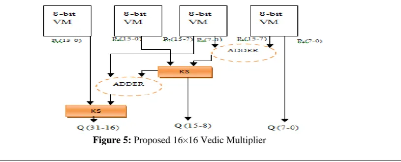
PROPOSED ARCHITECTURE OF 16X16 BIT VEDIC MULTIPLIER
The multiplication of two numbers is done by using Urdhwa Triyakbhyam. Here first the least significant bits of the two digits are multiplied. Then the intermediate digits are cross multi-plied and added together. After this the most significant digits are multiplied.
For the 16X16 bit multiplication small block of 2X2 or 4X4 or 8X8 multiplier were used in parallel to make the process easy and efficient.
bits. This is how the 32bit output is achieved in the less possible time.
IV.
RESULTS AND DISCUSSION
All the designing and experiment regarding algorithm that we have mentioned in this paper is being developed on Xilinx 14.1i updated version. Xilinx 9.2i has couple of the striking features such as low memory requirement, fast debugging, and low cost. The latest release of ISETM (Integrated Software Environment) design tool provides the low memory requirement approximate 27 percentage low. ISE 14.1i that provides advanced tools like smart compile technology with better usage of their computing hardware provides faster timing closure and higher quality of results for a better time to designing solution. ISE 14.1i Xilinx tools permits greater flexibility for designs which leverage embedded processors. The ISE 14.1i Design suite is accompanied by the release of chip scope ProTM 14.1i debug and verification software. By the aid of that software we debug the program easily. Also included is the newest release of the chip scope Pro Serial IO Tool kit, providing simplified debugging of high-speed serial IO designs for Virtex-4 FX and Virtex-5 LXT and SXT FPGAs. With the help of this tool we can develop in the area of communication as well as in the area of signal processing and VLSI low power designing.
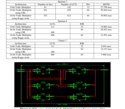
Table I: Comparison Results Of 8-Bit Vedic And 16-Bit Vedic Multiplier
Spartan-3
Architecture Number of slice Number of LUTs IOs MCPD 8-bit Vedic Multiplier 81 142 32 27.798 nsec 16-bit Vedic Multiplier
using CBL
361 629 64 50.562 nsec
16-bit Vedic Multiplier using Kogge stone
352 612 64 30.892 nsec
Spartan-6
Architecture LUTs IOB
8-bit Vedic Multiplier 111 32 19.885 nsec
16-bit Vedic Multiplier
using CBL 488
64 28.453 nsec
16-bit Vedic Multiplier using Kogge stone
468 64 21.591 nsec
Vertex-7
Architecture LUTs IOB
8-bit Vedic Multiplier 111 32 8.941 nsec
16-bit Vedic Multiplier
using CBL 488
64 13.157 nsec
16-bit Vedic Multiplier using Kogge stone
468 64 9.866 nsec
Figure 7: Output Waveform of the 16-bit Vedic Multiplier
Table 2: Comparisons Result for different types of design
Proposed Design Slices Slice Flip Flop
Number of 4-input LUTs
MP (ns)
Manoranjan Pradha et al.
3582 1024 6693 73.682 nsec
Amina Naaz et al. 3517 1024 6682 58.924 nsec Proposed Fast FIR
Filter
2782 892 5786 59.329 nsec
Figure 8: RTL view of proposed 3×3 parallel FIR filter using Kogge stone adder
Figure 9: Bar graph of the existing and proposed design
V.
CONCLUSION
The proposed 16x16 Vedic multiplier architecture has been designed and synthesized using on Spartan 3 XC3S400 board and is used in parallel FIR filter design. The proposed Vedic
[4]. S. S. Kerur, Prakash Narchi, Jayashree C N, Harish M Kittur and Girish V. A., “Implementation of Vedic Multiplier for Digital Signal Processing,” International Conference on VLSI ,Communication & Instrumentation (ICVCI), 2011.
[5]. G.Vaithiyanathan, K.Venkatesan, S.Sivaramakrishnan, S.Sivaand, S.Jayakumar, “Simulation and implementation of Vedic multiplier usingVHDL code,” International Journal of Scientific & Engineering Research, vol.4, 2013.
[6]. Pushpalata Verma and K. K. Mehta, “Implementation of an Efficient Multiplier based on Vedic Mathematics Using EDA Tool,” International Journal of Engineering and Advanced Technolog(IJEAT), vol.1, June 2012.
[7]. C. Cheng and K. K. Parhi, “Furthur complexity reduction of parallel FIR filters,” in Proc. IEEE ISCAS, May 2005, vol. 2, pp. 1835–1838.
[8]. C. Cheng and K. K. Parhi, “Low-cost parallel FIR structures with 2-stage parallelism,” IEEE Trans. Circuits Syst. I, Reg. Papers, vol. 54, no. 2, pp. 280–290, Feb. 2007.
[9]. J. G. Chung and K. K. Parhi, “Frequency-spectrum-based low-area low-power parallel FIR filter design,” EURASIP J. Appl. Signal Process., vol. 2002, no. 9, pp. 444–453, Jan. 2002.
[10]. K. K. Parhi, VLSI Digital Signal Processing systems: Design and Implementation. New York: Wiley, 1999.
[11]. Nivedita A. Pande, Vaishali Niranjane, Anagha V. Choudhari, “ Vedic Mathematics for Fast Multiplication in DSP,” International Journal of Engineering and Innovative Technology (IJEIT) ,vol.2, 2013.