An Efficient Technique for Design of Electrically Thick
Differentially-Driven Probe-Fed Microstrip Antennas
Cristiano B. De Paula1, *, Daniel C. Do Nascimento2, and Ildefonso Bianchi2
Abstract—This paper presents a computationally efficient technique for designing electrically thick differentially-driven rectangular microstrip antennas with coaxial probe feed. It concerns the use of a transmission line model for probe positioning, along with a full-wave field simulator that yields accurate results with reduced number of required full-wave simulations. An electrically thick antenna was designed with the proposed technique to operate at 2442 MHz, having its radiation patterns and input impedance measured and compared against a single-feed rectangular microstrip antenna to demonstrate the advantages of using differential feed to reduce cross-polarization inH-plane.
1. INTRODUCTION
A well-known bandwidth enhancement technique for microstrip antennas is increasing substrate thickness, but single-probe thick microstrip antennas present higher level of cross-polarization in H -plane [1, 2]. In order to suppress cross-polarized components, a differentially-driven microstrip antenna was proposed by [3]. The use of a pair of feed probes excited with currents of equal amplitude and opposite phases contributes to a symmetric radiation pattern in the E-plane [4]. These are advantages in comparison with the single-feed microstrip antenna. Moreover, in the case of a dual-polarization radiator with two pairs of feeds employed, the mutual coupling of each pair of feed is reduced, which results in higher isolation between antenna ports [2]. These characteristics are relevant for a radiator employed as the array element in a sector antenna for mobile communication systems, since these systems usually employ polarization diversity [5].
Recent works developed on differentially-driven microstrip antennas were reported [6–10], and expressions for calculating the input impedance were presented, but none of these works addressed the design of electrically thick antennas using efficiently full-wave field simulators for model optimization. Such works rely mainly on the classical method of cavity model [11], and no expressions for the impedance shift due to probe inductance were presented, though it is known that probe feed presents high inductance in thick substrates [2], making it difficult to match the antenna and its feeding transmission line. Besides, as already pointed out in [12], the use of an approximate method as the cavity model or transmission line model results only in the initial geometry, requiring a full-wave field analysis for model optimization in order to obtain accurate results, which brings the need of having an algorithm for the afterward model optimization, otherwise the design process becomes cumbersome. Therefore, in order to improve the efficiency of computational resources usage by reducing the number of full-wave simulations required to achieve the design goals, it was proposed the use of an adaptive transmission line model for probe-positioning via circuital analysis and an algorithm for its use, along with the full-wave simulator [12]. In the present work, this technique was extended for differentially-driven microstrip antennas and a specific adaptive transmission line model is presented. Finally, an antenna prototype for ISM Band (2.4–2.5 GHz) was constructed and its input reflection coefficient and
Received 3 November 2014, Accepted 26 November 2014, Scheduled 4 December 2014 * Corresponding author: Cristiano Borges de Paula ([email protected]).
radiated patterns were measured and compared with those of a single-feed microstrip antenna in order to validate the design technique and highlight the advantages of the differentially-driven microstrip antenna regarding its low cross-polarization inH-plane.
2. DESIGN PROCEDURE
Consider a probe-fed microstrip antenna with a rectangular patch of lengthLand widthW positioned on the surface of a dielectric substrate of thicknesshs, lengthLg, widthWg, relative permittivityεr and loss tangent tanδ. The ground plane is underneath the substrate and covers the entire bottom surface, being the impedance reference plane. The geometry is depicted in Figure 1, along with the adopted coordinate system.
(-d ,0, 0)p L
W
Lg
Wg hs
x
y z
(d , 0, 0)p
Figure 1. Geometry of the proposed antenna.
The coaxial feed probes are two SMA connectors, not depicted in the figure, positioned underneath the substrate. The center conductors of the SMA connectors are inserted into the substrate and have contact with the patch at coordinates (dp, 0, 0) and (−dp, 0, 0), where dp is the probe distance to the patch center. The model optimization process requires scaling the antenna dimensions in order to adjust its center frequency, which makes it convenient to write both the probe position and the patch width as functions of the patch length [12]. Hence, the probe distancedp can be written as
dp =RpL, 0< Rp≤0,5, (1)
and the patch width can be written as
W =RL, R≥1, (2)
whereRp is the control variable that sets the positions of probes, andRis the control variable that sets the desired geometry of the patch (square, rectangular). Microstrip antennas constructed for this work presented rectangular patch shape withR= 1.3.
During the model design optimization, variableLis adjusted to tune the antenna (change its center frequency) andRp is adjusted to match it, i.e., minimize the reflection coefficient magnitude at the input ports of the antenna.
For the initial geometry,Rp = 0.25 and the patch length is
L1= c0 2f0√εr,
(3)
where the index 1 indicates the first iteration of a series of L values during model optimization, c0 is the speed of the light in free space and f0 is the antenna desired center frequency.
Considering that the antenna has two feed probes, it is a 2-port device, and it can be described by its impedance matrix obtained by full-wave simulation,
V1
V2
=
Z11 Z12
Z21 Z22
I1
I2
where V1 and V2 are the voltages, and I1 and I2 are the currents of antenna coaxial feed probes at the reference plane. Since the antenna model is symmetric resulting Z11 =Z22, [Z] corresponds to a reciprocal network that yields Z12 =Z21, and the antenna will be fed differentially, i.e., I1 =−I2, the active input impedance is the same in both coaxial feed probes at the reference plane and can be written as
Zi =Z11−Z12. (5)
It is considered that the antenna feeding network will be implemented by a 3 dB 180◦ hybrid coupler, Balun, or power splitter to feed both probes with equal amplitude and opposite phases through transmission lines with convenient lengths and characteristic impedance Z0. Thus, probes positions need to be adjusted through proper control of the variable Rp in order to match each feed probe to its respective transmission line. The magnitude of the active reflection coefficient for each probe at reference plane is written as
|Γ|=Zi−Z0
Zi+Z0
. (6)
For the sake of simplicity, considering an ideal 3 dB 180◦ hybrid coupler as the feeding network, it can be easily calculated that the magnitude of reflection coefficient at the Δ port of the coupler when both coupled ports are terminated on Zi impedances yields |Γ|. Therefore, it is possible to consider the reflection coefficient of a single port during the design of the antenna as the one that would be obtained from the differentially-driven microstrip antenna with its feeding network. If the antenna is directly fed by a balanced circuit, the differential impedance is twice Zi, since Zi is the impedance relative to ground.
In order to reduce the number of full-wave simulations and save computer resources, probe positioning is performed only using circuital analysis. This is accomplished by using a circuital model that can predict the active impedance locus for different probe positions and it will be described in the next session. At this point, it is necessary to define the resonant frequency fr since electrically thick microstrip antennas may not present a null reactance [1]. The same definition as that used by [12] will be adopted here, which can be written as
|Γ(fr)|= min
f |Γ(f)| for f ∈ [f1, f2], (7)
where [f1, f2] is the frequency range of both full-wave and circuital simulations. For electrically thick microstrip antennas, the simulation frequency range has been set to [0.8f0, 1.2f0]. The goal of probe positioning is to adjustRp such as |Γ(fr)| ≤Γmin, where Γmin is a desired specification, e.g., it may be specified that |Γ(fr)| ≤ −30 dB. But, despite the fact the antenna is matched after tuningRp, fr may be different from the desired valuef0, thus patch length scaling is performed by a factor given byfr/f0 until the resonance frequency offset is within given specification limits. Every time a patch scaling is performed, a new full-wave simulation is executed for verification, and if needed, a new iteration of the algorithm is performed.
3. ADAPTIVE TRANSMISSION LINE MODEL (ATLM)
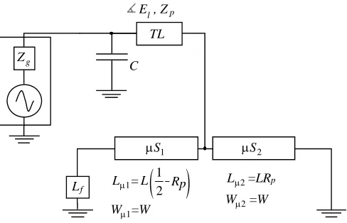
The circuital model used to predict the active antenna impedance locus is shown in Figure 2. It is composed by a generator with impedanceZg, a capacitor with capacitanceC, an ideal transmission line TLwith characteristic impedance Zp and electrical length (in degrees) given by
El = 360hs
c0
f√εr
−1
, (8)
where f is the simulated frequency, a first microstrip μS1 with length Lμ1 and width Wμ1, a second microstripμS2 with lengthLμ2 and widthWμ2 and a loadLf that is defined by its reflection coefficient Γf written as
Γf = (a0+a1f)e−j(b0+b1f), (9)
Lf
1
μS μS2 TL
C
1 2 p
L L
W =W
μ1
μ1
= L =LRp
W =W
μ2
μ2
p
E , Z
g
Z
R
( )
l
Figure 2. Adaptive transmission line model for the differentially-driven microstrip antenna.
In order to possibly use this model to adjust Rp and make |Γ(fr)| ≤ Γmin, first it is necessary to synthesize it to obtain an accurate impedance locus. This can be accomplished using a Gradient optimization tool, usually available in circuit simulators, to calculate C, Zp and the constants a0, a1,
b0 and b1 to fit the circuital model impedance locus to the one obtained in the full-wave simulation. Since the circuital model adapts its input impedance to fit the one from full-wave simulation, it is an adaptive model per nature and it was named ATLM — Adaptive Transmission Line Model [12]. Initial values are: a0 = 0.5, a1 = 0 s, b0 = 0.5,b1 = 0 s, Zp = 100 Ω, C= 0 pF and Rp is set to the same value used on the full-wave simulation model. During the synthesis, the generator impedance is given by
Zg =Zi∗, (10)
where the superscript ∗ denotes the complex conjugate operator, and Zi is the full-wave simulation active impedance. The same goals used by [12] for the circuital model synthesis are used here. They are the following:
Re{Zf}>0, (11)
Im{Zf}<0, (12)
whereZf is the impedance of the loadLf and
|Γ| ≤ ⎧ ⎪ ⎪ ⎪ ⎨ ⎪ ⎪ ⎪ ⎩
−30 dB, f ∈
f0−f 2−f1
4
,
f0+f 2−f1
4
−20 dB, f /∈
f0−f2−f1 4
,
f0+f2−f1 4
. (13)
Goals (11) and (12) are constraints in order to obtain a solution meaningful from a physical standpoint, if we consider that the loadLf corresponds to an equivalent slot located at the patch edge, and impedance
Zf is the radiation impedance, similar to the previously proposed transmission lines models [13, 14], in which the slot admittance was employed and calculated by approximated expressions. Goal (13) defines the level of accuracy desired between simulated impedance locus from circuital model and full-wave data, since in practice it is difficult to obtain equal impedance loci with both models.
Once the constants a0, a1, b0, b1 and parameters C and Zp are calculated and the generator impedance is changed such asZg =Z0, the circuital model is able to predict with high level of accuracy the impedance locus that would be obtained if the probe position varied in the full-wave model, which is the key feature that allows one to use the circuital model to optimizeRpinstead of running additional full-wave simulations.
4. ANTENNA DESIGN
To illustrate the design technique, one differentially-fed rectangular microstrip antenna was designed and a prototype was built for operation at center frequencyf0 = 2442 MHz. It was specified a fractional impedance bandwidth of at least 5% for VSWR≤2. It was decided to use the ArlonR CuClad 250 GX substrate, whose characteristics are εr = 2.55, loss tangent tanδ = 0.002 and height hs = 6.35 mm. At resonance, the maximum admissible magnitude of reflection coefficient was−30 dB, i.e., Γmin=−30 dB, and the maximum frequency error allowed for the final iteration of the algorithm was 0.25%. Antenna feed network characteristic impedance is Z0 = 50 Ω. Antenna dimensions are Lg = Wg = 100 mm and coaxial probe feeds are two SMA connectors. With this set of specifications, an initial model was simulated in MWS CSTR software, a full-wave field simulator, with R = 1.3, L1 = 38.47 mm,
Rp1= 0.25, in which indexes indicate the first iteration of the algorithm. With these parameter values, one can observe|Γ(fr)|=−16.6 dB. This result is shown in Figure 3.
Because at the first iteration of the design |Γ(fr)|>Γmin probe positioning was required and the ATLM was synthesized with L1 = 38.47 mm and Rp1 = 0.25, since the ATLM must be synthesized with the same antenna dimensions used for full-wave simulation. Its parameters were derived using a Gradient optimization tool, available at Agilent ADSR software, a circuit simulator, and the following parameter set was found: C = 0.21 pF, Zp = 99 Ω, a0 = 0.60, a1 = 6.83×10⁻¹¹s, b0 = −0.72 and
b1 = 7.65×10⁻¹¹s. As shown in Figure 4, the active impedance locus obtained by circuital simulation fits very well the active locus from full-wave data. Then, probe positioning was done using the ATLM resultingRp2 = 0.21,fr = 2225 MHz and|Γ(fr)|=−34 dB. With this resonance frequency, patch length scaling was done by a factor of 0.911, resulting L2 = 35.05 mm. As the patch length was changed, a new full-wave simulation was done after updating model parameters. It was found|Γ(fr)|=−39 dB at
fr= 2408 MHz, hence antenna matching was according the desired specification and probe positioning was not required, but resonance frequency was offset by −34 MHz, which yields a frequency error of 1.4%, higher than the admissible value. Therefore another patch length scaling was needed, resulting
L3 = 34.56 mm.
A third iteration full-wave simulation of the design algorithm yielded |Γ(fr)| = −34 dB at
fr = 2438 MHz, which meets all design requirements. The prototype was constructed based on the dimension values obtained from the design, and presentedfr= 2424 MHz,|Γ(fr)|=−35 dB, in addition to a fractional bandwidth of 7% (BW = 169 MHz). The active impedance was calculated based on its
Z parameters (derived from its measured S parameters) using (5).
2000 2100 2200 2300 2400 2500 2600
-40 -30 -20 -10 0
|
Γ
| dB
Freq [MHz] L = 38.47 mm e R = 0.251 p1
L = 35.05 mm e R = 0.212 p2
L = 34.56 mm e R = 0.213 p2 Prototype
Figure 3. Magnitude of reflection coefficient of full-wave simulations and experimental data based on active impedanceZi.
0.2 0.5 1.0 2.0 5.0
-0.2j 0.2j
-0.5j 0.5j
-1.0j 1.0j
-2.0j 2.0j
-5.0j 5.0j
Rp=0.25 Full-wave simulation
Rp=0.25 Synthesized ATLM
Rp=0.21 Optimized probe position
5. EXPERIMENTAL RADIATED RESULTS AND DISCUSSION
In order to demonstrate the advantage of using differential feed to reduce the cross-polarization level in
H-plane, a second antenna was used as reference. This antenna was fabricated on the same substrate, but it is a single-feed rectangular microstrip antenna with the following parameters: L = 34.79 mm,
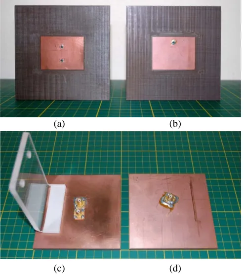
Rp = 0.34, Lg =Wg = 100 mm, R = 1.3. It was designed to have the same center frequency, and the measured magnitude of reflection coefficient was |Γ(fr)| = −31 dB at fr = 2427 MHz. Its fractional bandwidth is 7% [15]. Prototypes of differentially-driven and single-probe antennas are shown on Figure 5. As one can observe, the single-probe microstrip antenna, designed to operate at the same frequency as that of the differentially-driven antenna, has a probe positioned farther from the center of the patch. This implies that, as the substrate is made thicker, and consequently the impedance locus shift is more pronounced and more inductive, the probe will approach the edge of the patch first for the single-probe microstrip antenna. As a result, antenna matching will not be possible, first for the single-probe and followed by the differential feeding technique, therefore it is possible to use thicker substrates for differentially-driven microstrip antennas and obtain improved impedance bandwidth.
(a) (b)
(c) (d)
Figure 5. Prototypes: (a), (c) differentially-driven microstrip antenna, (b), (d) single-probe microstrip antenna.
The differentially-driven antenna required a feeding network that was constructed with a Mini-circuitsR power splitter (ZAPD-4-N+) and RG 223/U cables with different lengths to ensure 180◦phase difference at the antenna coaxial feeds. Measured phase unbalance was 2◦ and amplitude unbalance was 0.1 dB at 2442 MHz. Insertion loss between the common port and the first antenna port was 4.30 dB and between the common port and the second antenna port was 4.20 dB. Thus, the feeding network presented a differential insertion loss of 1.24 dB.
0 30 60 90 120 150 180 210 240 270 300 330
(a) Eφ (b) Eφ (b) Eθ
-40 -30 -20 -10 0 -30 -20 -10 0 dB
Figure 6. Full-wave simulation radiated patterns for copolar (Eφ) and crosspolar (Eθ) fields in H -plane (-planeY Z) at 2442 MHz: (a) differentially-driven microstrip antenna, (b) single-probe mi-crostrip antenna. 0 30 60 90 120 150 180 210 240 270 300 330 0
(a) f=2400 MHz
(a) f=2442 MHz
(a) f=2500 MHz
(b) f=2400 MHz
(b) f=2442 MHz
(b) f=2500 MHz
-40 -30 -20 -10 0 -30 -20 -10 dB
Figure 7. Measured copolar (Eφ) radiated pat-terns in H-plane (plane Y Z): (a) differentially-driven microstrip antenna, (b) single-probe mi-crostrip antenna. 0 -40 -30 -20 -10 0 -30 -20 -10 0 dB 0 30 60 90 15 180 210 240 270 300 330
(a) f=2400 MHz
(a)f=2442 MHz
(a) f=2500 MHz
(b) f=2400 MHz
(b) f=2442 MHz
(b) f=2500 MHz
Figure 8. Measured crosspolar (Eθ) radiated patterns inH-plane (planeY Z): (a) differentially-driven microstrip antenna, (b) single-probe microstrip antenna.
of the front-to-back ratio for the differentially-driven antenna. Antenna gain at 2442 MHz was 7.3 dBi and 8.3 dBi for differentially-driven and single-probe types, respectively (measurement uncertainty was 0.9 dB for the anechoic chamber used). The observed difference of gain may be attributed to the feeding network used for the differentially-driven microstrip antenna.
6. CONCLUSION
An efficient technique for designing electrically thick differentially-driven probe-fed microstrip antennas was presented, and a prototype with 7% fractional bandwidth was designed with the proposed technique, having its radiated patterns measured and compared with those of a conventional single-probe microstrip antenna. The design was proved to be computationally efficient as it required only three full-wave simulations in order to achieve the desired goals. Additionally, based on the comparison of the differentially-driven and conventional single-probe antenna designs it was found that differential feeding technique allows the design of thicker matched antennas. Such a conclusion is due to the fact that in single-probe microstrip antennas, the probe is located farther from the center of the patch, which becomes a limitation for antenna matching as substrate height is increased. Finally, the radiated patterns inH-plane for the differentially-driven antenna showed a significant cross-polarization reduction of 18.2 dB.
REFERENCES
1. Chang, E., S. A. Long, and W. F. Richards, “An experimental investigation of electrically thick rectangular microstrip antennas,” IEEE Trans. Antennas Propag., Vol. 34, No. 6, 767–772, Jun. 1986.
2. Huang, J., “Microstrip antennas: Analysis, design, and application,” Modern Antenna Handbook, 157–200, C. A. Balanis (ed.), Wiley, Hoboken, 2008.
3. Chiba, T., Y. Suzuki, and N. Miyano, “Suppression of higher modes and cross polarized component for microstrip antennas,” IEEE Antenna and Propagation Society Int. Symp., Vol. 2, 285–288, Albuquerque, Piscataway, 1982.
4. Petosa, A., A. Ittipiboon, and N. Gagnon, “Suppression of unwanted probe radiation in wideband probe-fed microstrip patches,”Electronics Letters, Vol. 35, No. 5, 355–357, Mar. 1999.
5. Fujimoto, K., “Antennas for mobile communications,” Modern Antenna Handbook, 1143–1228, C. A. Balanis, Ed., Wiley, Hoboken, 2008.
6. Zhang, Y. P. and J. J. Wang, “Theory and analysis of differentially-driven microstrip antennas,” IEEE Trans. Antennas Propag., Vol. 54, No. 4, 1092–1099, Apr. 2006.
7. Zhang, Y. P., “Design and experiment on differentially-driven microstrip antennas,” IEEE Trans. Antennas Propag., Vol. 55, No. 10, 2701–2708, Oct. 2006.
8. Zhang, Y. P., “Electrical separation and fundamental resonance of differentially-driven microstrip antennas,”IEEE Trans. Antennas Propag., Vol. 59, No. 4, 1078–1084, Apr. 2011.
9. Tong, Z., A. Stelzer, and W. Menzel, “Improved expressions for calculating the impedance of differential feed rectangular microstrip patch antennas,”IEEE Microw. Wireless Compon. Letters, Vol. 22, No. 9, 441–443, Sep. 2012.
10. Zhang, Y. P. and Z. Chen, “The Wheeler method for the measurement of the efficiency of differentially-driven microstrip antennas,” IEEE Trans. Antennas Propag., Vol. 62, No. 6, 3436– 3439, Jun. 2014.
11. Richards, W. F., Y. T. Lo, and D. D. Harrison, “An improved theory for microstrip antennas and applications,” IEEE Trans. Antennas Propag., Vol. 29, No. 1, 38–46, Jan. 1981.
12. Ferreira, D. B., C. B. de Paula, and D. C. do Nascimento, “Design techniques for conformal microstrip antennas and their arrays,” Advancement in Microstrip Antennas with Recent Applications, 3–31, A. Kishk, Ed., InTech, Rijeka, 2013, Doi: 10.5772/53019.
13. Munson, R. E., “Conformal microstrip antennas and microstrip phased arrays,” IEEE Trans. Antennas Propag., Vol. 22, No. 1, 74–78, Jan. 1974.
14. Derneryd, A. G., “A theoretical investigation of the rectangular microstrip antenna,” IEEE Trans. Antennas Propag., Vol. 26, No. 4, 532–535, Jul. 1978.