e-ISSN: 2278-067X, p-ISSN: 2278-800X, www.ijerd.com
Volume 11, Issue 11 (November 2015), PP.35-43
35
Efficient Method of Static Power Reduction by Using Biasing and
Body Biasing Techniques
Karanam Deepak
1, Sandeep Chittem
21M.Tech Student, Department of Elctronics & Communication Engineering, Chalapathi Institute of Technology,
Mothadaka, Guntur DT A.P, India.
2Assistant professor, Department of Electronics & Communication Engineering, Chalapathi Institute of
Technology, Guntur DT A.P, India,
Abstract:- A new multiple power-off modes power gating method was presented which can decrease the leakage power through short periods of inactivity. But, this method effects from high compassion to process variation, which impede manufacturability. Hence a new power-gating method is tolerant to method variation as well as scalable to further two intermediate power-off modes is needed. We propose body biasing technique used multimode power switches to decrease the static power and robust to process variations. The proposed devise require a smaller amount of design attempt and offer larger power reduction and lesser area cost than the previous method. Then we comparatively the result analysis the existing and proposed methods is simulated results of power values are also mentioned as shown in table. The proposed method also explains the advantage of simplicity and design effort. Then the proposed method is robust to process of variations and operates in two or more power off modes.
Index Terms:- Multi-mode VTCMOS switches, Leakage power, Power Consumption reduction, Reconfigurable power-gating structure.
I.
INTRODUCTION
As CHIP density increase obstinately beside Moore’s law, the power consumption is rising as a major trouble for existing systems [1]. The Dynamic energy is directly proportional to the square of the deliver voltage. Thus, a smaller voltage intensity yields a quadratic reduce in the energy consumption. To further decrease the dynamic power, systems-on-chip (SoCs) are partition into Voltage Island with divide supply rail and unique power characteristics [2]–[4]. Furthermore, as devices stay reduction, the channel distance end to end shorten and the gate oxide width reduces, rising the gate-induced drain leakage, the gate oxide tunneling current, and the junction leakage [5]. Several techniques have been offered in the text for reducing static power. Single frequent approach is to produce the circuit use dual-Vt libraries [6]. The High-Vtcell decrease the leakage
current at the expenditure of reduced performance; therefore their make use of on noncritical circuit domain reduce the leakage Power significantly without disturbing circuit performance. one more method exploit the information that the leakage power inspired by each gate powerfully depends on the input vector useful at the gate. Therefore, in order to decrease static power, it controls the contribution vector and the inside state of the circuit throughout period of idleness. Different technique decrease peak rush current. A particular category of this technique reduce the huge current rush by using one intermediary power off mode, while the methods existing in and affect a three step wake-up process. Intermediate power-off modes defeat an additional drawback of power switches, i.e., the moment in time required for getting better from the idle mode, referred to as the wake-up time.
Long wake-up time prohibit the make use of power switches throughout short periods of idleness. In adding present be application to be able make use of static power savings in part of the scheme provide with the purpose of these parts be capable of wake up fast upon request. The extended wake-up time of power switches prohibit their make use of in such cases too. In particular, these systems require that the memory elements (flip-flops) are required to particular logic values previous to the creation of a power-off mode. To concentrate on proposed a novel flip-flop design (the phase-forcing flip-flop) to make sure that all interior gate nodes in the combinational logic will be enforced to conventional state throughout the power-off mode. This novel flip-flop is not accessible in general typical cell libraries, which restrictions the applicability. In addition, the zigzag topology requires that, for every power supply, a couple of rails is circulated inside the regular cells (Vdd and
Vddv as well as Vss and Vssv, where Vddv is the virtual Vdd rail and Vssv is the virtual ground rail). These constraints
significantly increase the area overhead.
36
power rails and additional bypass switches. The techniques proposed require the intelligent position of keeper on chosen circuit lines. Moreover the added overhead, the keeper cannot be simply placed in non expected structure. The author planned a configuration with intermediary power-off mode, which reduces the wake-up time at the expense of reduced leakage current control. Comparable structures were proposed. The author extensive this exchange between wake-up transparency and leakage power savings into various power-off modes. Using these technique, as a substitute of consuming power by remain in the active mode throughout the small periods of idleness, the circuit is set keen on an suitable power-off mode (i.e., low-power state), which is find out by mutually the wake-up time and the length of the idle period. The longer the phases of inactivity, the higher are the power savings achieve by means of the majority violent power-off approach that can be tolerate.
Even although the structural design proposed is efficient for dropping leakage power throughout short periods of idleness, it has more than a few drawbacks that maximum value its applicability. First, it cannot be effortlessly extensive to maintain additional than two intermediary power-off modes and therefore it cannot fully use the power reduction prospective of the power-gating construction, particularly for high-performance circuit. Instant, the structural designs consume a important quantity of power, and this reduce the payback existing by the power switches.
CMOS
0 0 0 VGND
ILCORE
M0 M1 MP
IMO IM1 IMP
VDD
a) Multi mode operation in Snore mode
CMOS
1 0 0 VGND
ILCORE
M0 M1 MP
IMO IM1 IMP
VDD
b) Multi mode operation in Dream mode
CMOS
0 1 0 VGND
ILCORE
M0 M1 MP
IMO IM1 IMP
VDD
c) Multi mode operation in Sleep mode Figure: 1power gating Architectures by using Multi-Modes:
a) Snore mode b) Dream mode c) Sleep mode
Third, this construction is especially susceptible to process variations, which be able to harmfully have an effect on its manufacturability and preventability. Finally, it is not simply testable, as it consists of analog apparatus. In this paper, we present an efficient body biasing structural design that has none of the above drawback of the structural design proposed. The proposed construction require minimum propose effort since it is extremely easy, and by means of no analog components. It is significantly less important than the structural design proposed and offer superior power savings for related wake-uptimes.
The proposed structural design is as well additional tolerant to process variations; therefore its operation is new predictable. Lastly, a reconfigurable description of the projected construction is also planned, which can tolerate constant better process variations; enable thus the consumption of the proposed structural design for newer technology. The organization of the have a rest of this paper is as follow part II presents backdrop substance to position the proposed employment in a suitable framework. Part III introduces the proposed body biasing structural design, the design technique, and the reconfigurable structural design. Part IV presents an estimation of the proposed structural design, including comparison with before work. In lastly, part V concludes this paper.
II. BACKGROUND
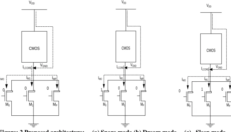
In the Figure. 1 represents Multiple-modes of power gating methods. It consists of the major power switch transistor MP also two tiny transistors M0 and M1, every one subsequent to an intermediary power-off
high-Vt transistor and it remains on simply throughout the active mode of operations. Transistors M0 and M1 are
minute low-Vt transistors so as to be turned on simply throughout the equivalent power-off mode. (i.e., M0 is turned on throughout the dream mode and M1 is turned on throughout the sleep mode).
In proposed scheme, VTCMOS procedure threshold voltage of low threshold devices is various by apply changeable substrate bias voltage from a organize circuit
1. In raise in the lower threshold voltage, devices lead improved sub threshold leakage and therefore additional standby power utilization.
2. To decrease static power decrease is to use short supply voltage and short threshold voltage not including lose speed presentation.
3. It provides power in decrease only 10%. Try. It has most important advantages.
III. BODY BIASING TECHNIQUE
A. Proposed Architecture
In the Figure.2 shows the proposed method of design. It consists of having of the major power switch transistor MPand two little transistors M0 and M1, each consequent just before an intermediary power-off mode
(M0 is represents to the dream mode and M1 represents to the sleep mode). Transistor MPbe a high-Vt threshold
transistor and it remaining on just throughout the active mode. Transistors M0 and M1 are small low-Vt
transistors as a result as to be turned on simply throughout the equivalent power off mode of methods. (i.e., M0
switch is turn on during the dream mode and M1 switch is turned on during the sleep mode). A variety of modes
of process are as follows.
1) Active Mode: The Transistors MP, M0, M1 are on in the circuit.
2) Snore Mode: In addition to the Transistors MP,M0, and M1 are in the switches are in off state as revealed in
Fig. 2(a). In this mode, the leakage current of the core, I Lcore, is equal to the collective leakage current flows from side to side transistors M0, M1, MP(I Lcore = I LM0 + I LM1 + I LMP). In which there is a very small (we
know that M0, M1 be tiny transistors and MPis a high- Vttransistor). Therefore the voltage level at V_GND is
close to Vdd and the circuits consume a insignificant quantity of power, other than the wake-up time is high comparatively on previous method.)
3) Dream Mode: In the Transistor M0 is on and transistors MPand M1 are off as exposed in Fig. 2(b). In this
mode the current flowing from side to side transistor M0 (In addition to therefore the collective current flows
from side to side M0, M1 and Mp)increases since M0 is on (IMO > I LM0). The severe worth of IM0 based on the
chip size of transistor M0, and it set the virtual ground node at a voltage level stage which can be lower than Vdd
(i.e., VV_GND< Vdd). Therefore the Static power dissipated by the core is high compare to thesnore mode, other than the wake-up time is a smaller amount.
4) Sleep Mode: in this case the Transistor M1 is on, and MP, M0 are off as exposed in Fig. 2(c). By providing the transistor M1 has better characteristic ratio than M0 (Wm1/Lm1> Wm0/Lm0), they have the same opinion MP
increases still extra when M1 is on (note thatIM1> IM0). so, the voltage level at the virtual earth node is further
reducing compare to the dream mode and therefore the wake-up time decreases at the expenditure of increased power use ate current graceful through M0, M1.
CMOS
0 0 0 VGND
ILCORE
M0 M1 MP
IMO IM1 IMP
VDD
CMOS
1 0 0 VGND
ILCORE
M0 M1 MP
IMO IM1 IMP
VDD
CMOS
0 1 0
VGND
ILCORE
M0 M1 MP
IMO IM1 IMP
VDD
38
B. Design MethodIn this proposed technique of Body biasing has be established to exist efficient in address procedure inconsistency in a combination of easy chip design. However, for contemporary microprocessor ICs with several cores and active voltage (V)/frequency (F) scaling (DVFS), By using of body bias method has important implication. In support of a 16- core chip-multiprocessor implement in a better-performance of 22 nm technology, the body biases essential to get together the frequency objective at the lowest and highest voltage(V)/frequency(F) level be special by an middling of 0.7 V, imply that per-level bias are compulsory to totally influence body biasing. The requires to create unexpected changes in the body biases after the voltage/frequency level changes affects the cost and benefit examination of body biasing schemes. It is established that compute the single body biases for each voltage/frequency level at chip power-on offers the most excellent exchange among a selection of methods in conditions of area, performance and power.
Whereas incessantly adjust the body biases throughout procedure offer improvement in energy/efficiency, these advantages be outweighed by the execution costs. The performance costs of constantly adjust the body biasing methods are conquered by the settling time of the controller. In the Present controllers are calculated for easy general-purpose microprocessors and it is not optimize for settling time, and require D/A converters with elevated time constants. We propose method a fully-analog controller that is able to attain considerably lower settling time for a permanent area and power than earlier controllers. By way of the proposed method of controller, constantly compute the body biasing offer a improved transaction in terms of area, performance, and power than computes only one of its kind body biasing method for every voltage(v)/frequency(f) stage on chip power-on. Further development in energy (E)/efficiency can be achieves through an included come up to body biasing method and DVFS. Since VDD is scale and body biasing has unusual effects on static vs. dynamic power, the working point yielding the lowly on the whole power is dependent on the proportion of full amount power due to leakage. Escape power, in turn, is powerfully influenced by procedure of variations.
C. Body Biasing
In the Body biasing technique is one more method of civilizing energy/efficiency, by reclaims performance gone to margins due to variation. Subsequent to fabrication procedure, the variable threshold voltage (VTH) of transistors can be modulating by shifting the body-to-source voltage. In size MOSFETs, the
VTH is specified by:
0
2
2
TH TH F BS F
V
V
V
(1) Wherever the VTH0 is the apparatus threshold voltage by means of no body bias useful, 2ΦF is the outside potential at physically powerful inversion, and γis the body effect coefficient. For effortlessness, we observe this expression for the casing of an NFET with the source joined to ground. If a negative voltage is useful to apply on the body then the collapse width increases, which way that a better gate voltage is essential to form an inversion coating and thus the VTH increase; this method is recognized as a reverse body biasing method (RBB).
In the same way, if a positive voltage is useful to apply on the body while the source is stranded, then the exhaustion width decreases, and therefore the VTH decrease; this is recognized as a forward body bias (FBB). all through this effort, VBSn and VBSpwill stand for the body to source voltage of NFETs and PFETs,
correspondingly. Negative values of this parameter will point out RBB and a positive individual FBB, in spite of which direction the body-to-source voltage should really be shift. There be more than a few technology issues with body biasing in immensity MOS RBB increase small channel property, which increases changeability inside strategy distribution a bias. This is particularly difficult in circuits that are susceptible to device alike, such as SRAMs. FBB improve short channel effects, but as well increases connection leakage, potentially to the peak wherever the source-to bulkiness T-junction is further biased.
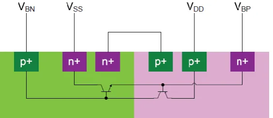
In the addition of, an analog pointer, the body bias, should be dispersed a important detachment – in the great, crosswise the entire die. This becomes more and more difficult with scaling since cross-talk stuck between wires worsens. To end with, the compassion of VTH to the body bias decrease by means of scale, since the guide doping increase. Body biasing is partial in the amount of the VTH modify that can be induce. The highest forward-bias is partial by current flows diagonally the P-N junction produced between the n type -well and p-type well. A thyristor-like instrument is created in the substrate by the two bipolar transistors, as shown in Figure 3 establish that present be no latch-up consequence FETs.
39
n-well and p-well. A thyristor-like device is produced in the substrate through the two bipolar transistors, as exposed in Figure 3 Oowaki et al. establish that present was no latch-up effect by means of up to 0.5 V forward bias [ (assumed by Miyazaki et al. , Tachibana et al. , and Narendra et al. . The greatest reverse-bias is imperfect by elevated leakage and potential break-down crosswise the reverse biased drain body junction, above all during burning. The compassion of threshold voltage to the body bias for NFETs and PFETs is exposed in Figure for the 90 nm, 45 nm, and 22 nm analytical technologies. While the sympathy of VTH to the body biases do the reduce as technology scales, the decrease from 90 nm to 22 nm. (4 technology generations) is only 12% for the NFET and 10% for the PFET.
Figure 3: Leakage path in forward body biasing
IV.
EVALUATION AND COMPARISONS
In this sector, we explain that simulation results in addition to comparison beside other technique easily reached in the literature.
Result analysis and Comparisons Using a Large Logic Core (by using biasing and body biasing techniques):
The aim of the primary section is to estimate the proposed technique after it is apply to great logic cores so as to be dissimilar in volume to real design from industry. To this end, we explain the present simulation results going on a large logic core consisting of 9 million transistors. This core consists of numerous inverters of different sizes which are determined by a mixture of input vectors. Yet though it is not a genuine circuit, it is representing of a reasonable industrialized circuit in conditions of static power consumption throughout dc operation in power-off mode. We use the 45-nm analytical technology by means of 1.1-V power supply.
The leakage power utilization of the core in inactive mode through no power gating is equivalent to 10 mW. All simulations were completed by using the Synopsis HSpice simulation engine. And also we are note that, since the use of a various method of core by means of high opinion as well as unlike new parameters (such as the technology, the voltage surroundings, and the input vector), we cannot in a straight line evaluate the experimental results of our technique with the results accessible. Hence, we implement equally the structural design [see Fig. 1(c)] and the proposed structural design (see Fig. 2) for the aforesaid logic core. As optional, the width of the major power switches. (Transistor denoted as MP).
Table I: Static power dissipation
Mode of
operation
Power dissipation
values for
Existing Method
(µw)
Wake up
time (ns)
Power dissipation
values for
Proposed Method
using Body Biasing
(µw)
Wake up
time (ns)
Snore Mode
25
µw
31.15 ns
0.00001 µw
39.10
ns
Dream Mode
35.3111
µw
28.56
ns
26.74 µw
32.5
ns
40
And the results values are set to be equivalent to 12% of the total width of the n MOS transistors in the logic core. For the logic core that can we use, the width/length relation of transistor MP is calculate as equal to 43.2 × 10⁶ nm/45 nm and it is implement as the parallel correlation of a amount of smaller transistors. In categorize to supply fair evaluation; the transistor size in together architectures were chosen in such a way as (a) to be of least amount of size essential and (b) to present related wake-up times, in together architectures. In dream and sleep mode the power dissipation is equal, as no more than one transistor is in on mode in the set of connections apart beginning core logic. Furthermore, in the proposed design, the size of transistors M0 and M1 have be elected in such a approach as to offer the same voltage level at the virtual ground node by means of the scheme proposed at every one power-off mode and designed for the similar input vector. Thus, the logic core consumes the same quantity of static power in both architectures at every power-off mode. For pattern, allowing for an input vector that drive the two-thirds of the transistors to logic ―1‖ and the rest of the transistors to logic 0,‖ the voltage level at the V_GND node is equivalent to 217.1, 415.8, 541.8, and 668.5 mV at four intermediate power-off mode.
For together architectures, we suppose that the voltage at the V_GND node settle to the predictable value previous to the wake up procedure begins. In adding, the core is measured as fully prepared after the virtual ground node is discharge to the value of 1% of Vdd. First, we evaluate both architectures in conditions of area transparency calculated as transistor sizes. The width of transistors M0, M1 in the projected structure is equal to 250 and 480 nm, therefore, for comparison purposes; we excluded the overhead of these transistors from the above your head of together architectures. We are also prohibit that the decoder, as it is elective in both architectures and can be absent (we implement both scheme without the make use of of decoders). The rest of the circuit diagram in the proposed structural design occupy approximately one-fifth (1/4.8) of the area of the structural design and it is a reduced amount of than 0.0002% of the area of the core. Even however this is an estimation based on transistor sizes, it is obvious from Figs. 1(c) and 2 that the projected structural design is much simpler.
We can note that the scheme of proposed maintain simply single midway power-off mode, it is indicate as vision for evaluation purposes. The final three rows demonstrate the amount of cycles that are desirable for wake up the core starting every power-off mode so as to be support through each technique. The primary two columns near the results for together a higher –variable threshold Vt and low variable threshold Vt parker transistor projected. The consequently two columns close by the results for the high-Vt and low-Vt parker transistor projected. We embedded four dissimilar biasing voltages, 0v, −0.2v, −0.4v, and −0.6v for both the high- variable threshold Vt and low variable threshold Vt parker transistor projected but the results were almost the same (apart from for the sleep mode anywhere the static power somewhat varied between 0.9456 mW and 0.96 mW as reported in Table I). The after that two columns nearby the results for configurations Conf. 1 and Conf. 2 that are use.
41
V.
RESULTS ANALYSIS
In following figures are explains as given below a Snore Mode, Dream Mode, Sleep Mode, Input and output waveforms of a biasing and body biasing techniques. When input is high, output is low. The wave forms can represented in x-axis time and in y-axis voltage.
A) BIASING RESULTS
Fig4: Snore Mode Operation of a biasing technique
Fig5: Dream Mode Operation of a biasing technique
42
Fig7: Active Mode Operation of a biasing technique
B) BODY BIASING RESULTS
Fig8: Snore mode with body bias
Fig9: Dream mode with body bias
43
VI.
CONCLUSION
We describe that a method of a Body biasing scheme so as to provide many power-off modes. The proposed method of design obtainable the benefit of ease and required least amount design effort. General simulation results shows that, in the difference to a current power-gating method, the projected plan is robust to process of difference and it is scalable to a more than the two powers off modes. Furthermore, it requires considerably less area and consumes much less power than the existing design. In conclusion of a reconfigurable edition of this technique can be use to augment the manufacturability and robustness of the proposed method of design is in the technologies with better process variations.
REFERENCES
[1]. Semiconductor Industry Association. (2007) [Online]. Available:
http://www.itrs.net/Links/2007ITRS/Home2007.htm
[2]. D. Lackey, P. Zuchowski, T. Bednar, D. Stout, S. Gould, and J. Cohn, ―Managing power and performance for system-on-chip designs using voltage islands,‖ in Proc. IEEE/ACM Int. Conf. Comput. Aided Design, Nov. 2002, pp. 195–202.
[3]. R. Puri, D. Kung, and L. Stok, ―Minimizing power with flexible voltage islands,‖ in Proc. IEEE Int. Symp. Circuits Syst., May 2005, pp. 21–24.
[4]. R. Puri, L. Stok, J. Cohn, D. Kung, D. Pan, D. Sylvester, A. Srivastava, and S. Kulkarni, ―Pushing ASIC performance in a power envelope,‖ in Proc. Design Autom. Conf., Jun. 2003, pp. 788–793. [5]. K. Roy, S. Mukhopadhyay, and H. Mahmoodi-Meimand, ―Leakage current mechanisms and leakage
reduction techniques in deepsubmicrometer CMOS circuits,‖ Proc. IEEE, vol. 91, no. 2, pp. 305–327, Feb. 2003.
[6]. S. Idgunji, ―Case study of a low power MTCMOS based ARM926 SoC: Design, analysis and test challenges,‖ in Proc. IEEE Int. Test Conf., Oct. 2007, pp. 1–10.
AUTHORS PROFILE
KARANAM DEEPAK Received the B.Tech degree in Electrical and Electronics Engineering from Prakasam Engineering College, Kandukuru, Prakasam (DT), A.P, India, in 2013. Currently he is pursuing M.Tech in VLSI & Embedded System Design from Chalapathi institute of Technology, mothadaka, Guntur (DT), A.P, India. Her research interests include Power Converters, and VLSI systems design.
CH SANDEEP Received the B.Tech degree in Electronics and Communications from Sri Chundi Ranganayakulu Engineering college, Guntur (DT), A.P, India. He has Completed M.Tech in Embedded Systems from Holy Mary institute of technology and science, Bogaram, Rangareddy (DT), Telangana, India. Currently he is working as Assistant professor in Chalapathi institute of Technology, mothadaka, Guntur (DT), A.P, India.