Modified Leakage Reduction Circuit using Self
Biasing Circuit
Jerin Varghese Jackson Abraham K. Thomas
PG Student Assistant Professor
Department of Electronics & Communication Engineering Department of Electronics & Communication Engineering Saintgits College of Engineering Saintgits College of Engineering
Susan Abe Professor
Department of Electronics & Communication Engineering Saintgits College of Engineering
Abstract
The MOSFET design was first introduced in 1960. Since then leakage current is a factor that have been a problem faced by the designers. Leakage current is a phenomenon that usually occurs in a semiconductor in which the mobile carriers flow through an insulated region. Leakage current causes extra consumption of power and larger power consumption may cause failure of the circuit. In this project in order to reduce the leakage current in logic circuits the method adopted is based on a self biasing circuit. In this method conventional techniques of transistor stacking is used. More the number of transistors used for the stacking, more will be the amount of leakage current reduced. Self biasing circuit is provided to reduce the delay and overall power consumption.. Simulation of the circuit shows that along with the leakage current reduction, delay between input and output, power consumption were reduced compared to existing conventional techniques
Keywords: Leakage Current, Stacked Transistors, Self Biasing Circuit.
________________________________________________________________________________________________________
I.
I
NTRODUCTIONMOSFET design was successfully demonstrated in 1960. Since then this small semi conductor device has revolutionised technology. The MOSFET devices have been subjected to aggressive scaling over the past decades. Typical MOSFET channel lengths were once several micrometres, but modern integrated circuits are incorporating MOSFETs with channel lengths of tens of nanometers (ITRS, “International technology roadmap for semiconductors,” 2005). Robert Dennard's work on scaling theory was pivotal in recognizing that this ongoing reduction was possible. Intel began production of a process featuring a 32 nm feature size in late 2009.
With this came the concept of reducing the channel length of the device. The reasons behind this were several. Often smaller MOSFETS are preferred. One of the main reason includes by reducing the size of the transistors more and more number of transistors can be included in a given chip area. This results in providing with a chip which can perform more functionality within its same given area. Since fabrication costs for a semi conductor wafers are relatively fixed, the number of chips that can be produced per wafer estimates the cost of integrated circuits. Now here lies the advantage of smaller ICs. They allow more chips to be manufactured on a wafer thereby reducing price per chip. In fact, over the past 30 years the number of transistors per chip has been doubled every 2–3 years once a new technology node is introduced (ITRS, “International technology roadmap for semiconductors,” 2005).
Producing MOSFETs with channel lengths much smaller than a micrometreis a challenge, and the difficulties of semiconductor device fabrication are always a limiting factor in advancing integrated circuit technology. Certain difficulties faced by the designers were high sub threshold conduction, increased gate – oxide leakage, increased junction leakage, lower output resistance, interconnect capacitance, heat production. Among these leakage current has been a great issue to be dealt with by the designers. Several techniques have been used to reduce this considerably.
In this report a leakage reduction technique is used, in which we rely up on both conventional and a new biasing circuit in order to reduce the leakage current, over all delay and also the total power dissipation
II.
L
ITERATURE REVIEWLeakage Current: A.
MOSFET scaling deep into the sub-100-nmregime has resulted in substantially greater leakage power consumption compared to a few generations ago (ITRS, “International technology roadmap for semiconductors,” 2005). In semiconductor devices, leakage is a quantum phenomenon where mobile charge carriers (electrons or holes) tunnel through an insulating region. Leakage increases exponentially as the thickness of the insulating region decreases. Tunnelling leakage can also occur across semiconductor junctions between heavily doped P-type and N-type semiconductors. Other than tunnelling via the gate insulator or junctions, carriers can also leak between source and drain terminals of a Metal Oxide Semiconductor (MOS) transistor. This is called sub threshold conduction. The primary source of leakage occurs inside transistors, but electrons can also leak between interconnects. Leakage increases power consumption and if sufficiently large can cause complete circuit failure.
Over the past years, the MOSFET has continually been scaled down in size. The MOSFET‟s that were once in micrometer length have been reduced to nanometer length.Smaller MOSFETs are desirable for several reasons. One of the most convincing reason is that reducing the size of transistors can be used to incorporate more transistors in to a given chip area. The other reason is that smaller the transistor size faster will be the switching time.
Technology scaling calls for a reduction of the supply voltage to restrain power density(S.Borkar, 1999).To maintain circuit performance while scaling, the threshold voltage of the device is also reduced. However, this causes the sub threshold current to increase exponentially since it is exponentially dependent on threshold voltage Vth (S.Borkar, 1999). In addition to the sub threshold leakage current, gate tunnelling current also increases due to the scaling of gate oxide thickness (ITRS, “International technology roadmap for semiconductors,” 2005). Each new technology generation results in nearly a 30 times increase in gate leakage (K. Bernstein et al, 2003). Hence, it has become extremely important to develop design techniques to reduce static power dissipation during periods of inactivity.
Leakage Current Mechanisms: B.
For nanometre devices, leakage current is dominated by sub threshold leakage, gate-oxide tunnelling leakage and reverse-bias p-n jup-nctiop-n leakage(Paulo Frap-ncisco Butzep-n ap-nd Rep-nato Perez Ribas, 2007).
Supply voltage has been scaled down to keep dynamic power consumption under control. Threshold voltage was also scaled in order to provide high drive current capability. While the transistor is working in weak inversion region there will be a current flow between the drain and source, known as subthreshold current i.e., the gate voltage is lower than the Vth.
There are two components in subthreshold current. They are drift current and diffusion current. In a mosfet transistor when the gate to source voltage is more than the Vth it is said to be working in strong inversion region. At this point of work mode t he drift current component is the dominant portion. When it comes to weak inversion region, there won‟t be any minority carrier concentration which is almost zero. At this mode of operation the channel won‟t be having any horizontal electrical field. Instead the channel will be exhibiting a small longitudinal electric field as a result of drain-to-source voltage. In this situation, the movement of the carriers will be between source and drain of the MOSFET by diffusion. Therefore, the subthreshold current is owned by diffusion current and the relation between this current and both gate-to-source and threshold voltage is exponential (Paulo Francisco Butzen and Renato Perez Ribas, 2007). In short channel devices, as the channel length is reduced there will be a tendancy for both source and drain depletion regions to advances significantly into the channel region and thereby influencing the field and potential profile inside that. These are known as short channel effects (SCE). SCE reduce transistor threshold voltage due to phenomenon like channel length reduction (Vth roll-off) and the DIBL increasing. This results in significant subthreshold current in short channel devices (SOUDRIS, D. et al, 2002)
As mentioned before, the scaling down of the channel length in to nanometre scale has increased the phenomenon of short channel effects. This includes effects like DIBL and Vth roll-off. So it clearly states that short channel effects are meant to be controlled. To attain this oxide thickness must be become thinner as the scaling technology advances. Aggressive scaling of the oxide thickness, gives rise to high electric field. High electric field helps in a direct tunnelling current to flow through the gate insulator.
Gate oxide tunnelling current is the phenomenon in which either the electrons or holes move from bulk and source-drain overlap region via the gate oxide potential barrier and into the gate. This can also happen in vice-versa direction. There are three major gate leakage mechanisms in a MOS structure. In the first one, the electrons will be tunnelling from conduction band of the substrate to the conduction band of the gate or vice-versa. This is known as Electron Conduction-Band tunnelling (ECB). The second one is the Electron Valence-Band tunneling (EVB). Here, electrons tunneling takes place between the valence band of the substrate and the conduction band of the gate. The final one is known as Hole Valence-Band (HVB) tunneling, where holes tunneling from the valence band of the substrate to the valence band of the gate (or vice- versa) (Paulo Francisco Butzen and Renato Perez Ribas, 2007)
and „p‟ regions get heavily doped. During such a mode of operation band-to-band tunneling (BTBT) leakage will dominate the reverse biased p-n junction leakage mechanism.
A high electric field across a reverse biased p-n junction causes a current flow through the junction due to tunneling of electrons from the valence band of the p-region to the conduction band of the n-region
Band-to-band tunneling leakage, negligible in current processes when compared to the subthreshold and gate oxide leakages. But it should be taken into account in 25nm technologies (MUKHOPADHYAY, S. et al. 2005)
The junction tunneling current depends exponentially on the junction doping and the reverse bias across the junction. Forward body bias can be used to reduce the band-to-band tunneling leakage.
Leakage Reduction Techniques: C.
To suppress power consumption in low-voltage circuits, it is necessary to reduce leakage power in both active and standby modes. Reduction in leakage current can be achieved by using both process and circuit level techniques. At process level, leakage reduction can be achieved by controlling the dimensions (length, oxide thickness, junction depth, etc.) and doping profile in transistor (Paulo Francisco Butzen and Renato Perez Ribas, 2007)
Dual threshold CMOS is a static technique that exploit the delay slack in non-critical paths to reduce leakage power. It provides both high and low threshold voltage (Vth) transistors in a single chip that are used to deal with the leakage problem. High Vth transistors suppress the subthreshold current, while low Vth transistors are used to achieve high performance. For a logic circuit, the transistors in non-critical paths can be assigned high Vth to reduce subthreshold leakage current, while the performance is not sacrificed by using low Vth transistors in the critical paths (WEI, L. et. Al.1999).
Power gating technique uses the power supply voltage as the primary source for reducing leakage current. It refers to using a MOSFET switch (sleep transistor) to cut off, or gate, a circuit from the power rails (Vdd and/or gnd) during standby mode. The power gating switch typically is positioned as header between the circuit and the power supply or as footer between the circuit and the gnd. During active operation, the power gating switch remains on, supplying the current that the circuit uses to operate. During standby mode, turning off the power gating switch reduces the current dissipated through the circuit. Turning off the sleep transistor provides leakage reduction for two primary reasons. First, the width of the sleep transistor is usually less than total width of transistors being gated. The smaller width provides a linear reduction in the total current drawn from supply node during standby mode. Secondly, leakage currents diminish whenever stacks of transistors are off due to the source biasing effect (BUTZEN, P. F. et al2006).
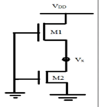
Subthreshold leakage current flowing through a stack of series connected transistors reduces when more than one transistor in the stack is turned off. This effect is known as “stacking effect”. The leakage of a two-transistor stack is about an order of magnitude less than the leakage in a single transistor (Paulo Francisco Butzen and Renato Perez Ribas, 2007). Fig 1 shows the transistor stacking technique.
Fig. 1: Two NMOS Off-Transistor Stack
III.
A
NALYTICAL PROCEDURESConventional Method using Power Gating: A.
During standby mode, turning off the power gating switch reduces the current dissipated through the circuit. In the conventional design, there will be a power gated transistor which is placed at the virtual ground point of the main circuit. The main circ uit being used here is a 28T transistor full adder. The conventional circuit controls the steady-state virtual ground rail potential by modulating the gate voltage of footer device. In sleep mode the footer device is always biased in weak inversion region. The circuit along with the footer transistor is shown in Fig 2
Fig. 2: A 28 T Transistor Full Adder Circuit Design With Power Gating
Conventional Method using Transistor Stacking: B.
Connecting series of transistors serially to the virtual ground point is generally known as transistor stacking.Subthreshold leakage current flowing through a stack of series connected transistors reduces when more than one transistor in the stack is turned off. This effect is known as “stacking effect”. It can be better understood with the following Fig 3.5 of a two transistor stack.
Fig. 4: Full Adder circuit with Transistor Stacking
The above circuit in Fig 4 also utilises the delay network to induce delay on the stacked transistors so that the ground bounce is brought to minimum.
Proposed Method using Self Biasing Circuit: C.
The conventional methods have their own advantages and disadvantages. The sleeper technology produced a better reduced over all delay and total power dissipation whereas it failed to reduce the leakage current as anticipated. The stacked transistors were successful in reducing leakage current as compared to sleeper transistors, but the ground bounce value and over all delay was increased. So tradeoffs exist in both technology as a result there comes in a new method which have minimized the tradeoffs to a whole new level.
A new circuit is being introduced along with the conventional techniques, the circuit is called biasing circuit. The biasing circuit is in Fig.5.
The working of the circuit is as follows: Transistors M1, M2, and M3, all equally sized, form a current mirror, biased by the VGS of M1. The currents in each leg ofthis circuit then should nominally be the same. However, sincetransistors M5 and M6 as well as transistors M7 and M8 formstacked paths, and since transistors M4–M7 are all equally sizedwhile M8 is larger, the currents through each leg of the currentmirror are different.
The output of the circuit is taken across device M7. Transistor M8 can be sized appropriately dependingon the necessary bias output needed. As noted previously, transistorsM1 through M3 are equally sized and transistors M4through M7 are equally sized, though different than the pmos devices. Transistor M8 is used to generate an appropriate Vbias
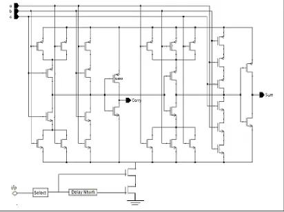
The circuit is mainly designed to reduce the overall delay. The biasing circuit combined with the conventional stacking transistors will produce the results with minimum tradeoffs. Fig.6 shows the proposed design.
Fig. 6: Proposed Circuit With Conventional And Self Biasing Technique
The conventional method used here is transistor stacking because as the number of stacked transistors is increased the rate at which the leakage current reduced will be more. The RLC circuit used here is for measuring the ground bounce voltage causing extra spikes in the output.
IV.
R
ESULTS AND DISCUSSIONIn order to understand the effectiveness of the proposed design, the performance of the proposed design is evaluated against the conventional design. The compared designs include full adder with power gating technique and full adder with stacking technique. The Pyxis schematic of Mentor Graphics is used in order to create the schematics of the circuit. The performances of both conventional and proposed designs are evaluated through pre-layout simulations using eldo simulator. The output waveforms are viewed using E-Z wave viewer. The target technology is the TSMC 180-nm CMOS process.The operating condition used in simulations is 500 MHz/1.8V. In order to analyze the power consumption data pattern with 100% transition probability is given at a temperature of 27oC.
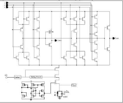
Proposed Circuit with Conventional and Self Biasing Circuit: A.
Fig. 7: Proposed Circuit with Conventional and Self Biasing Circuit
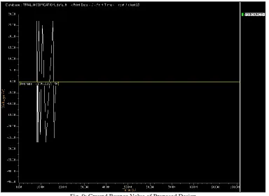
Fig. 9: Ground Bounce Value of Proposed Design
The leakage current was estimated for all circuits. First for the 28 transistor full adder with power gated transistor then for the full adder with the stacked transistors and finally for the proposed design with self biasing circuit. The inputs for all the circuit was A=1 B=0 and Cin=1. During this input transition, the OFF state transistors was noted and its leakage current was calculated The total power dissipation was obtained from the log sheet of the simulator. The delay was calculated by measuring the difference between Cin ¬and Cout. The wave forms were plotted using E-Z wave viewer.
All the results are incorporated in Table 5.1. From the table its very much clear that the proposed design outperforms both conventional designs. Total power dissipation has dropped from nano watts to pico watts. There is a 47% reduction in overall delay. A 2.5% reduction in leakage current.
Table -1
Performance Comparison between Conventional and Proposed Designs Parameters
Circuit Design
Conventional design with Power Gated technique
Conventional design with stacked transistors
Proposed Design Total Power
Dissipation 308.9752 nW 127.7316 mW 119.55869 pW
Overall Delay 90.858 ps 168.69 ps 43.193 ps
Leakage current 1.6 nA .08 nA .04 nA
Ground Bounce 89.3515 nV 17.625 mV 106.2395 nV
V.
C
ONCLUSIONInvention of MOSFET was great revolution in technology. From its discovery until this time it has been subjected to scaling. Small transistors have always its advantages but along with it came the problem of leakage current. This problem happened to be dominant in every small transistor design. So there came the importance of leakage reduction and its corresponding techniques. Selecting appropriate technique for your design is very important. There are number of techniques which can be used to reduce the leakage current. Some of the techniques include usage of power gated transistor, stacked transistors and so on.
The results show that the proposed design can be used to in circuit designs were power dissipation, leakage current and delay are major concerns.
R
EFERENCES[1] Abdollahi, F. Fallah, and M. Pedram, “An effective power mode transition technique in MTCMOS circuits,” in Proc. ACM/IEEE Des. Autom. Conf., 2005, pp. 37–42.
[2] AGARWAL, A. et al. Leakage Power Analysis and Reduction: Models, Estimation and Tools, Proc. IEE, v.152, n.3, p 353-368, May 2005 [3] AGARWAL, A. et al. Leakage Power Analysis and Reduction for Nanoscale Circuits, IEEE Micro, Los Alamitos, v.26, n.2, p 68-80, Mar. 2006 [4] K. Bernstein et al., “Design and CAD challenges in sub-90 nm CMOS technologies,” in Proc. Int. Conf. Comput.-Aided Des., 2003, pp. 129–136
[5] R. Bhanuprakash, Manisha Pattanaik and S.S.Rajput “Reduction Of Leakage Current And Ground Bounce Noise Using High Performance Stacking Power Gating Logic Circuits,” proceedings of IEEE Singapore,pp 1-6,2009.
[6] S.Borkar,“Designchallengesoftechnologyscaling,”IEEEMicro,vol. 19, no. 4, pp. 23–29, Jul./Aug. 1999.
[7] BUTZEN, P. F. et al. Leakage reduction technique for CMOS complex gates. In: SOUTH SYMPOSIUM ON MICROELECTRONICS, 21., 2006, Porto Alegre. Proceedings… Porto Alegre: Instituto de Informática, UFRGS, 2006, p.111-114
[8] CAO, K.M. et al. BSIM4 Gate Leakage Model Including Source-Drain Partition.In: INT. ELECTRON DEVICES MEETING, 2000. Digest of Technical Papers, Dec. 2000, p. 815818.
[9] CHEN, Z. et al. Estimation of Standby Leakage Power in CMOS Circuits Considering Accurate Modeling of Transistor Stacks. In: INT. SYMP. LOW POWER ELECTRONICS AND DESING, ISLPED, 1998. Proceedings…, New York: ACM SIGDA, 1998, p.239244.
[10] GUINDI, R. S.; NAJM, F. N. Design techniques for gate-leakage reduction in CMOS circuits. In: INT. SYMP. QUALITY ELECTRONIC DESIGN, 2003. Proceedings…, IEEE, 2003, p.61-65
[11] Harmander Singh, Member, IEEE, Kanak Agarwal, Member, IEEE, Dennis Sylvester, Senior Member, IEEE, and Kevin J. Nowka, Senior Member, IEEE [12] ITRS, “International technology roadmap for semiconductors,” 2005. [Online]. Available: http://public.itrs.net
[13] S. Kim, S. Kosonocky, D. Knebel, and K. Stawiasz, “Experimental measurement of a novel power gating structure with intermediate power saving mode,” in Proc. Int. Symp. Low Power Electron. Des., 2004, pp. 20–25
[14] MUKHOPADHYAY, S. et. al. Gate Leakage Reduction for Scaled Device Using Transistor Stacking. IEEE Trans. on VLSI Systems, New York, v.11, n.4, p. 716-730, Aug 2003.
[15] MUKHOPADHYAY, S. et al. Accurate Estimation of Total Leakage in Nanometer-Scale Bulk CMOS Circuits Based on Device Geometry and Doping Profile. IEEE Trans. on CAD of IC and Systems, New York, v.24, n.3, p. 363-381, Mar. 2005
[16] NARENDRA, S. G.; CHANDRAKASAN, A. Leakage in Nanometer CMOS Technologies. New York: Springer, 2006. 307 p.
[17] S. Narendra, S. Borkar, V. De, D. Antoniadis, and A. Chandrakasan, “Scaling of stack effect and its application for leakage reduction,” in Proc. Int. Symp. Low Power Electron. Des., 2001, pp. 195–200
[18] PARK, J. C.; MOONEY III, V. J. Sleepy Stack Leakage Reduction. IEEE Transactions on VLSI Systems, New York, v.14, n.11, p.1250-1262, November 2006
[19] Paulo Francisco Butzen and Renato Perez Ribas Leakage Current in Sub-Micrometer CMOS Gates, 2007
[20] RAO, R. M. et al. Efficient techniques for gate leakage estimation. In: INT. SYMP. LOW POWER ELECTRONICS AND DESING, 2003. Proceedings…, New York: ACM, 2003, p.100-103
[21] ROY, K. et al. Leakage Current Mechanisms and Leakage Reduction Techniques in DeepSubmicrometer CMOS Circuits. Proceedings of IEEE, New York, v.91, n.2, p. 305-327, Feb 2003
[22] ROY, K.; PRASAD, S. C. Low-Power CMOS VLSI Circuit Design. New York: Wiley Interscience, 2000. 359 p.