IMPLEMENTATION AND
COMPARATIVE STUDY OF A HIGH
SPEED MULTIMODE DIGITAL
MODULATOR FOR POWER
CONSTRAINED DIGITAL
COMMUNICATION
SUMAN HALDARDepartment Of Electronics & Communication Engineering
Neotia Institute of Technology Management &Science, Sarisha, West Bengal-743368,India Email: [email protected]
cell:09830378118
SOUMITA HALDAR CHAKRABORTY Department Of Electronics & Communication Engineering
Neotia Institute TechnologyManagement&Science, Sarisha, West Bengal-743368,India Email: [email protected]
cell: 08145917560 PRADIPTAMAITI
Department Of Electronics & Communication Engineering Aryabhattya Institute of Engineering and Management Durgapur, India
Email:[email protected] PRATIK KUMAR SINHA
Department Of Computer Science Engineering
Neotia Institute of Technology Management &Science,Sarisha, West Bengal-743368, India Email: [email protected]
PIJUSH BISWAS Department Of Computer Science NSHM Knowledge Campus, Kolkata, India
Email: [email protected] Dr. AMITAVA SINHA
Department Of Electronics & CommunicationEngineering
Neotia Institute TechnologyManagement&Science, Sarisha, West Bengal-743368, India
Abstract:
In this paper, the architecture and implementation of a multimode digital modulator has been presented. The digital modulator can perform any one of Amplitude Shift Keying, Frequency Shift Keying, Phase Shift keying or Quadrature Phase Shift Keying modulation, de- pending on the value of the select inputs. The key feature of the work is reduced power and simple circuitry, without compromising throughput. Prototypes based on the proposed architecture have been developed. Analysis of the simulation reports validate correct functionality while synthesis and power reports show that the prototypes have very low power requirement while maintaining high throughput. Appropriate comparisons with other existing implementations, as reported in the literature, have also been included.
Keywords: Digital Communication, Multimode Modulator, High Speed Modulator, ASK, FSK, PSK, QPSK, FPGA.
1. Introduction
Universal digital modulators capable of operating in multiple modulation schemes have been the area of research for the past few years. Such universal modulators [1] become handy in applications where the underlying modulation scheme needs to be changed on the fly. As for example the baseband processing algorithms of an adaptive wireless communication may vary in accordance with change in environmental parameters, change in wireless communication standards and to provide better quality of service.
1.1 Brief review of previous work
The design of multimode modulators (the term universal modulator has been preferred by some group of researchers) has been explored mainly in two courses
Some researchers first identified the basic building blocks required for the different target modulation schemes and combined those building blocks to synthesize the multimode modulator with or without hardware optimization. Architecture of such a modulator for software defined radio have been reported in [2]. The architecture was reconfigurable and was realized using Field Programmable Gate Array (FPGA), but the problem of such architecture was that it was still too demanding for power and area constrained communication applications.
The second style of design that is implementation of universal modulators based on CORDIC algorithm and/or Direct Digital Frequency Synthesis (DDFS) has been discussed in [3], [4], [5], [6], [7], [8]. However the CORDIC based architectures are complex and with limited computation speed whereas the DDFS implementations suffer from limited operating range and limited spectral purity. In this context the current work focuses on the issue of design and implementation of a multimode digital modulator with less silicon area and reduced power consumption, suitable for area and power constrained digital communication while at the same time without compromising with the speed of operation.
In this paper the architecture of the proposed modulator has been detailed in section2. The architecture has been validated using Xilinx ISE V.14.2 on a Spartan 3E family FPGA board as well as using the Tanner EDA Tool. Such implementation issues are discussed in section 3. Results from the synthesis along with their analysis and comparison with other reported works have been included in section 4 and section 5 of the paper deals with concluding notes and future scope of the work.
2. Architecture of the proposed modulator
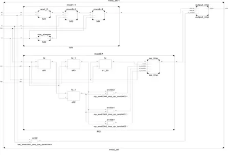
The block diagram of the proposed modulator has been presented in Fig. 1. It is a multimode modulator in the sense that it can operate in any one of the ASK, FSK, PSK and QPSK modulation mode depending on the value of the control signals S0 and S1. The modulator is made up of simple digital subcomponents like 2:1 multiplexers, binary inverters, AND gates, NAND gates, D flip flops and appropriate carrier and clock signals. Apart from the select and data inputs, the modulator requires two carrier signals (C1 and C2) and two clock signals (CLK0 and CLK1) as inputs. The total architecture is divided into two blocks. The upper block performs ASK, FSK and PSK modulation schemes whereas the lower block is for QPSK modulation. The principle of operation of the proposed modulator in various modulation modes and the corresponding values control signals has been discussed in the following subsections.
2.1 Operation of the proposed modulator in a ASK mode
The architecture works in ASK mode when the select inputs are set to 0 and 0 for S0 and S1 respectively. When S1 is 0, the output of AND1 is 0, which is connected to I0 of MUX1. As S0 is 0, regardless of the value of the input I1, the output of MUX1 will always be 0 which is connected to the input I0 of MUX2.
Fig.1 Block diagram of the proposed modulator
The input I1 of MUX2 is connected with the carrier signal C1 and the data input is connected to the select line. Depending on the value of binary data, either 0 or C1 will be propagated to the output of MUX2 and fed to the input I1 of MUX4. The select line of MUX4 is driven by the output of NAND1, which will be 1 when S1 and S0 are both 0. Thus, the final output will be the ASK modulated signal.
2.2 Operation of the proposed modulator in a FSK mode
When the control signals are set to 0 and 1 for S0 and S1 respectively, the carrier signal C2 is prorogated to the input I0 of MUX1 through AND1. The carrier signal C1 is connected to the input I1 of MUX2. Depending upon the binary data input, either carrier signal C1 or C2 will be selected as the output of MUX2 and will be propagated to the input I2 of MUX4. This value itself will be the final output of the circuit as the select input of MUX4, driven by NAND1, is 1.
2.3 Operation of the proposed modulator in a PSK mode
2.4 Operation of the proposed modulator in a QPSK mode
When the values of both control signals S0 and S1 are 1, the output of NAND1 is 0. In this case, the final output from MUX4 is driven by the input I0, which is the output of MUX3, from the lower block. QPSK modulation scheme requires four phase shifted carrier frequencies. In order to obtain these, the carrier C1 is passed through INV4, producing a 180 phase shifted version of C1. The original C1 is also connected to a D flip flop (DFF4) to obtain the 90 phase shifted carrier, which is again passed through INV5 to get the 270 phase shifted carrier. The four carriers thus obtained are connected to inputs I0, I2, I1 and I3 of MUX3 respectively. It must be noted that for the 90 and 270 phase shifting circuit to work as intended, the frequency of CLK0 must be exactly double the frequency of the carrier C1. The input binary data is passed through a serial to parallel converter to separate out the di-bits. The serial to parallel converter consists of DFF1, driven by CLK1, and DFF2 and DFF3, driven by the inverse of CLK1. The clock CLK1 must be synchronous to the input data. The separated di-bits are connected to the select inputs S0 and S1 of MUX3. Thus, depending on the value of the di-bits, one the four phase shifted carrier frequencies is selected as output of MUX3 which is also the final output obtained from MUX4.
2.5 Power saving feature of the proposed modulator
The proposed architecture has been made power efficient in two steps. First, as is commonly done, the number of components required and the interconnect circuitry has been kept minimal and simple. It can be deduced from the block diagram that the circuit requires five inverters, four one bit D flip flops, three 2x1 multiplexers, one 4x1 multiplexer, one two input logical AND and one two input logical NAND, which is a total of only 15 basic components. The interconnections amongst these components is also simple with minimal fan-out. Thus, power requirement and dissipation will be very low.
Second, the architecture has been such designed that during operation only the components necessary for the selected modulation scheme are supplied power and switched on. Specifically, when the logical NAND (NAND1) of the selects inputs S0 and S1 is high (as for ASK,PSK and FSK), the upper block is turned on while the lower block remains turned off and consumes negligible power. The reverse happens when the output of NAND1 is low (for QPSK) and the corresponding output of INV2 is high, which supplies voltage to the lower block. This turns on the lower block and the upper block remains unpowered.
3. Hardware Implementation
3.1 FPGA implementation of the proposed modulator
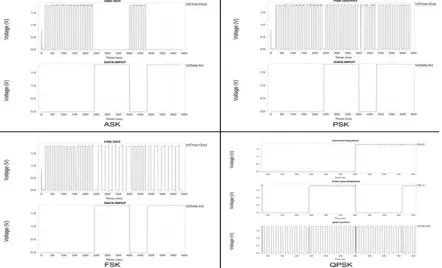
A prototype of the proposed architecture was developed for implementation on FPGAs. The Xilinx Virtex-5 and Spartan 3E FPGAs were selected as targets for the prototype. The architecture was described in VHDL and the code was synthesized using Xilinx Synthesis Tool (XST). The RTL schematic obtained after synthesis is shown in Fig. 2. A test bench was created to validate the functionality of the prototype and behavioral as well as post place and route level simulation was accomplished. The simulation was performed using Xilinx ISim Simulator. A portion of the waveforms obtained from I Sim during simulation is shown in Fig. 3 from where it can be seen that the prototype works as expected.
3.2 Implementation of the proposed modulator using Tanner EDA Tool
The prototype for the proposed architecture was designed using Tanner EDA Tool. The bottom up approach was used to develop the prototype. The basic gates were first implemented at the CMOS level and the other components were created using these basic gates. The design at the CMOS level ensured that all gates consist of minimal number of CMOS units. It was also ensured that the NAND and INV gates are capable of driving power to other components through their outputs. The final circuit of the prototype is shown in Fig. 4. The functionality of the prototype was tested by simulation and a portion of the obtained waveforms is provided in Fig. 5. The prototype was tested with 1.8V and 2.5V supply voltages and was found to be valid.
Fig. 2. FPGA schematic diagram of the proposed modulator
Fig. 4. Schematic diagram of the proposed modulator using Tanner EDA tool
Fig. 5. Simulated waveforms from the Tanner EDA tool implementation
4. Experimental Results and Analysis
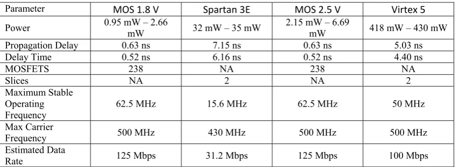
The two prototypes, one targeting FPGAs and the other with CMOS units were tested for their performance and power consumption and dissipation. The results obtained have been summarized in Table 1.
Table 1. Performance and Power Consumption Summary
Parameter MOS 1.8 V Spartan 3E MOS 2.5 V Virtex 5
Power 0.95 mW – 2.66 mW 32 mW – 35 mW 2.15 mW – 6.69 mW 418 mW – 430 mW
Propagation Delay 0.63 ns 7.15 ns 0.63 ns 5.03 ns
Delay Time 0.52 ns 6.16 ns 0.52 ns 4.40 ns
MOSFETS 238 NA 238 NA
Slices NA 2 NA 2
Maximum Stable Operating
Frequency 62.5 MHz 15.6 MHz 62.5 MHz 50 MHz
Max Carrier
Frequency 500 MHz 430 MHz 500 MHz 500 MHz
Estimated Data
Rate 125 Mbps 31.2 Mbps 125 Mbps 100 Mbps
The FPGA based prototypes were found to have a considerably larger power requirement. However, this is not a flaw of the design but is a drawback inher- ently associated with FPGAs. The explanation is twofold. Firstly, FPGAs have large static power requirements, which varies from one FPGA model to another, but in any case remains much higher than dedicated VLSI circuitry. Even if only a small portion of the FPGA is to be utilized, the whole reconfigurable area has to be powered up. There are some technologies used by FPGA vendors to con- trol this power dissipation. However, even those technologies cannot surpass the superiority of low power consumption of VLSI circuits. Secondly, the proposed architecture features a simple, but dynamic, power management circuitry which controls whether power is to be supplied to a component or not. However, since it is not possible to control the power supply to individual slices of FPGAs (from standard vendors), the FPGA based prototype lacks this feature. It must be noted that FPGA based prototype utilizes only two slices in both Virtex-5 and Spartan 3E implementations. This allows the modulator to be integrated with other designs (such as interleavers, encryption blocks etc.) with minimal impact on the overall design size.
The prototype designed at the CMOS level is capable of performing dynamic power management, hence consumes very less power. The added advantage of dedicated circuitry is low propagation and time to output delays.
The performance and power requirements of the proposed architecture was compared with the results reported in related literature [2], [3], [4], [5], [6], [7], [8]. Although a direct comparison could not be made, largely due to difference in the set of modulation schemes implemented in the existing work, it could be generally observed that the performance proposed architecture is at par or superior to them. Also, the power consumption reported in the existing work was found to be higher in all cases considered.
5.Conclusion
A multi-mode digital modulator was proposed and prototyped in this paper, with the target of achieving high throughput and very low power requirement. Two prototypes, one based on FPGAs and the other using CMOS units, were developed. The FPGA based design met the throughput expectations but had high power requirements. On the other hand, the CMOS based implementation met all expectations, including very low power requirement. This work can be further taken in two directions. One, other sets of related and relevant modulation schemes may be used with the same key targets. Two, the inherent problem of power management in FPGAs may be looked into. The scope of this work encompasses all digital communication requiring high speed and low power multimode modulators.
References:
[1] Meyer-Baese, U.: Digital Signal Processing with Field Programmable Gate Arrays. 4th edn. Springer Science & Business Media
(2014)
[2] Karmakar, A., Saha, A., Sinha, A.: On the Design of a Reconfigurable Radio Processor Using FPGA. Vol. 6. No. 2. International
Journal of Computer Theory and Engineering (2014)
[3] Kumar, S. A., Brahmaiah, V.P., Teja, L. D.: Universal Modulator using CORDIC Algorithm for Communication Application. Vol. 6.
Issue 6. International Journal of Advances in Engineering & Technology (2014) 2480-2488
[4] HariKumar, G., MadhuBabu, M.: FPGA implementation of universal modulator using CORDIC algorithm for communication
application. Vol. 6. Issue 11. Interna- tional Journal of Engineering Research and Development (2013) 08-14
[5] Sharma, N. S. M., Thrimurthulu, V.,Murthy, S. V. S. N., Rao, B. N., Anasuya, R.: Field Programmable Gate Array (FPGA)
[6] Kalra, P., Vemishetty, N., Venkatramani, B.: CORDIC based Universal Modula- tor. Proceedings of 2014 RAECS UIET Panjab University Chandigarh India. IEEE Xplore DOI: 978–1–4799–2291–8/14(2014)
[7] Nagaraju, P., Babulu, K., Sailaja, V.: VLSI Implementation and Performance Evaluation of Universal Modulator using CORDIC
Algorithm for Digital Communication Applications. Vol. 02. Issue 05/06. Progress In Science and Engineering Research Journal (2014) 39-47
[8] Kumar, M. S., Reddy, S. N.: FPGA implementation of universal modulator using CORDIC algorithm for communication
applications. Vol. 4. Issue 6. International Journal of Modern Engineering Research (2014) 63-71