ESD WARNING:Standard CMOS handling precautions should be observed to avoid static discharge.
Description
The 3.3 V HCMS-39xx family is similar to the 5.0 V HCMS-29xx family, except it operates at a lower operating voltage. Package dimensions and pin outs are exactly the same for both families. The product has been thoroughly characterized and stringent reliability tested to ensure that the product is of high quality.
Similar to the 5.0 V platform, this family product is a high performance, easy to use dot matrix display driven by on-board CMOS IC. Each display can be directly interfaced with a microprocessor, thus eliminating the need for cumbersome interface components. The serial IC interface allows higher character count information displays with a minimum of data lines. The easy to read 5x7 pixel format allows the display of upper case, lower case, Katakana, and custom user-defined characters. These displays are stackable in the x- and y-directions, making them ideal for high character count displays.
Features
• Easy to use• Interfaces directly with microprocessors
• 0.15” character height in 4 and 8 character package
• 0.20” character height in 4 and 8 character package
• Rugged X- and Y-stackable package
• Serial input
• Convenient brightness controls
• Wave solderable
• Low power CMOS technology
• TTL compatible
• 3.3 V operating voltage
Applications
• Telecommunications equipment
• Portable data entry devices
• Computer peripherals • Medical equipment • Test equipment • Business machines • Avionics • Industrial controls
HCMS-39x6 and HCMS-39x7
3.3 V High Performance CMOS
5x7 AlphaNumeric Displays
Data Sheet
HCMS-3906, HCMS-3966, HCMS-3916, HCMS-3976, HCMS-3907, HCMS-3967, HCMS-3917, HCMS-3977
Package Dimensions
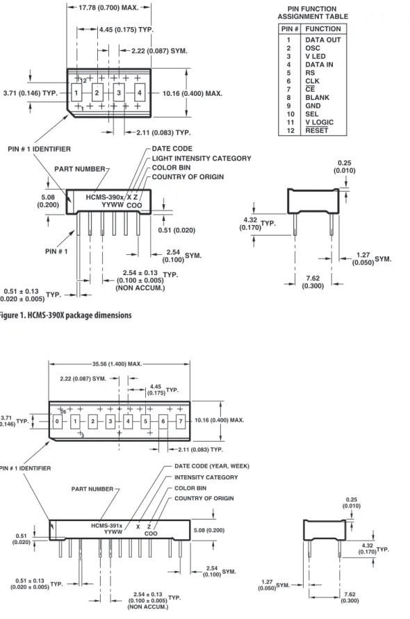
Figure 1. HCMS-390X package dimensions
X Z COO 2.11 (0.083) TYP. 0.25 (0.010) 7.62 (0.300) PIN # 1 IDENTIFIER 4 3 2 1 17.78 (0.700) MAX. 3.71 (0.146) TYP. 4.45 (0.175) TYP. 2.22 (0.087) SYM. 10.16 (0.400) MAX. PIN # 1
LIGHT INTENSITY CATEGORY DATE CODE COLOR BIN COUNTRY OF ORIGIN PART NUMBER 5.08 (0.200) 2.54 (0.100)SYM. TYP. 0.51 ± 0.13 (0.020 ± 0.005) 2.54 ± 0.13 (0.100 ± 0.005) (NON ACCUM.) TYP. 4.32 (0.170)TYP. 1.27 (0.050)SYM. 1 12 0.51 (0.020) DATA OUT OSC V LED DATA IN RS CLK CE BLANK GND SEL V LOGIC RESET PIN FUNCTION ASSIGNMENT TABLE 1 2 3 4 5 6 7 8 9 10 11 12 PIN # FUNCTION HCMS-390x YYWW 2.54 ± 0.13 (0.100 ± 0.005) (NON ACCUM.) TYP. 35.56 (1.400) MAX. 7 6 5 4 3 2 1 0 0.25 (0.010) 7.62 (0.300) PIN # 1 IDENTIFIER X Z COO INTENSITY CATEGORY DATE CODE (YEAR, WEEK)
COLOR BIN COUNTRY OF ORIGIN PART NUMBER 5.08 (0.200) 2.54 (0.100) SYM. 0.51 (0.020) TYP. 0.51 ± 0.13 (0.020 ± 0.005) 2.22 (0.087) SYM. 10.16 (0.400) MAX. 2.11 (0.083) TYP. 4.32 (0.170)TYP. 1.27 (0.050)SYM. 4.45 (0.175)TYP. 3.71 (0.146) TYP. NO PIN NO PIN V LED NO PIN NO PIN NO PIN GND LED NO PIN NO PIN V LED NO PIN NO PIN NO PIN DATA IN RS NO PIN CLOCK CE BLANK GND LOGIC SEL V LOGIC NO PIN RESET OSC DATA OUT PIN FUNCTION ASSIGNMENT TABLE 1 2 3 4 5 6 7 8 9 10 11 12 13 14 15 16 17 18 19 20 21 22 23 24 25 26 PIN # FUNCTION 3 26 HCMS-391x YYWW
Figure 2. HCMS-391X Package dimensions
Notes:
1. Dimensions are in mm (inches).
2. Unless otherwise specified, tolerance on dimensions is ± 0.38 mm (0.015 Inch). 3. Lead material: solder plated copper alloy.
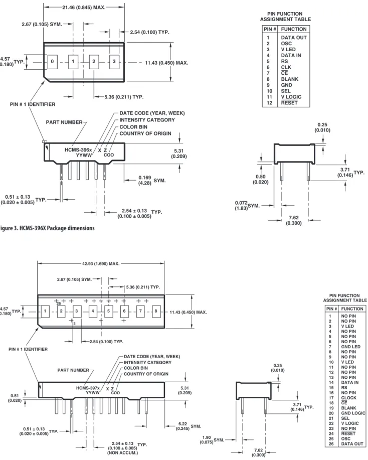
Figure 3. HCMS-396X Package dimensions
Package Dimensions,
continued3 2 1 0 PIN # 1 IDENTIFIER PART NUMBER 5.31 (0.209) 0.169 (4.28) SYM. TYP. 0.51 ± 0.13 (0.020 ± 0.005) 2.54 ± 0.13 (0.100 ± 0.005)TYP. 2.67 (0.105) SYM. 2.54 (0.100) TYP. 11.43 (0.450) MAX. 5.36 (0.211) TYP. 0.25 (0.010) 7.62 (0.300) 3.71 (0.146)TYP. 0.072 (1.83)SYM. 4.57 (0.180)TYP. X Z COO INTENSITY CATEGORY DATE CODE (YEAR, WEEK) COLOR BIN COUNTRY OF ORIGIN 21.46 (0.845) MAX. 0.50 (0.020) DATA OUT OSC V LED DATA IN RS CLK CE BLANK GND SEL V LOGIC RESET 1 2 3 4 5 6 7 8 9 10 11 12 PIN FUNCTION ASSIGNMENT TABLE PIN # FUNCTION HCMS-396x YYWW
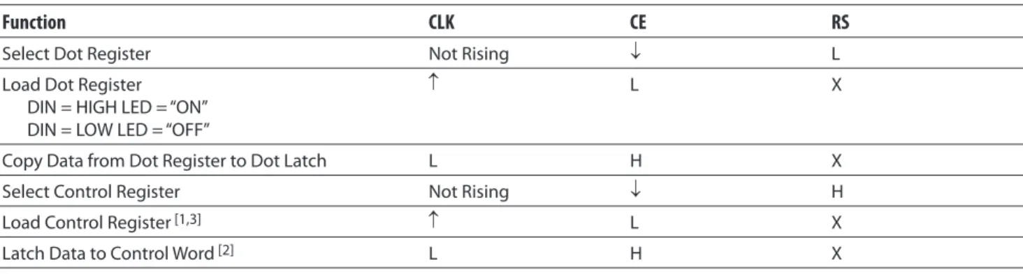
Figure 4. HCMS-397X Package dimensions
PIN FUNCTION ASSIGNMENT TABLE 8 7 6 5 4 3 2 1 X Z COO PIN # 1 IDENTIFIER INTENSITY CATEGORY DATE CODE (YEAR, WEEK)
COLOR BIN COUNTRY OF ORIGIN PART NUMBER 5.31 (0.209) 6.22 (0.245) SYM. 0.51 (0.020) TYP. 0.51 ± 0.13 (0.020 ± 0.005) 2.54 ± 0.13 (0.100 ± 0.005) (NON ACCUM.) TYP. 42.93 (1.690) MAX. 2.67 (0.105) SYM. 5.36 (0.211) TYP. 11.43 (0.450) MAX. 2.54 (0.100) TYP. 0.25 (0.010) 7.62 (0.300) 3.71 (0.146)TYP. 1.90 (0.075)SYM. NO PIN NO PIN V LED NO PIN NO PIN NO PIN GND LED NO PIN NO PIN V LED NO PIN NO PIN NO PIN DATA IN RS NO PIN CLOCK CE BLANK GND LOGIC SEL V LOGIC NO PIN RESET OSC DATA OUT 1 2 3 4 5 6 7 8 9 10 11 12 13 14 15 16 17 18 19 20 21 22 23 24 25 26 PIN # FUNCTION 4.57 (0.180)TYP. 3 26 HCMS-397x YYWW Notes:
1. Dimensions are in mm (inches).
2. Unless otherwise specified, tolerance on dimensions is ± 0.38 mm (0.015 Inch). 3. Lead material: solder plated copper alloy.
Device Selection Guide
Description Red Green
1 x 4 0.15” Character HCMS-3906 HCMS-3907
1 x 8 0.15” Character HCMS-3916 HCMS-3917
1 x 4 0.20” Character HCMS-3966 HCMS-3967
1 x 8 0.20” Character HCMS-3976 HCMS-3977
Absolute Maximum Ratings
Logic Supply Voltage, VLOGIC to GNDLOGIC ... -0.3 V to 7.0 V LED Supply Voltage, VLED to GNDLED ... -0.3 V to 5.5 V Input Voltage, Any Pin to GND ... -0.3 V to VLOGIC +0.3 V Free Air Operating Temperature Range TA[1] ... -40° C to +85° C Relative Humidity (non-condensing) ... 85%
Storage Temperature, TS ... -55° C to 100° C Soldering Temperature (1.59 mm (0.063 in.) below body)
Solder Dipping ... 260° C for 5 secs Wave Soldering ... 250° C for 3 secs ESD Protection @ 1.5 kΩ, 100 pF (each pin) ... Class 1, 0-1999 V TOTAL Package Power Dissipation at TA = 25° C[1]
4 character ... 0.766 W 8 character ... 1.532 W 16 character . ... 3.064 W
Note:
1. For operation in high ambient temperatures, see Appendix A, Thermal Considerations.
Recommended Operating Conditions over Temperature Range (-40° C to +85° C)
Parameter Symbol Min. Max. Units
Logic Supply Voltage[1] VLOGIC 3.1 5.5 V
LED Supply Voltage[1] V LED 3.1 5.5 V
GNDLED to GNDLOGIC[1] – -0.3 +0.3 V
Note:
Electrical Characteristics over Operating Temperature Range (-40° C to +85° C) Parameter Symbol TA = 25° C VLOGIC = 3.3 V -40° C < TA < 85° C 3.0 V < VLOGIC < 5.5 V
Units Test Conditions Typ. Max. Min. Max.
Input Leakage Current HCMS-390X/396X (4 char) HCMS-391X/397X (8 char) II +7.5 +15 -2.5-5.0 +50+100 µA VIN = 0 V to VLOGIC ILOGIC OPERATING HCMS-390X/396X (4 char) HCMS-391X/397X (8 char) ILOGIC (OPT) 0.4 0.8 2.55 510 mA VIN = VLOGIC ILOGIC SLEEP[1] HCMS-390X/396X (4 char) HCMS-391X/397X (8 char) ILOGIC (SLP) 5 10 1530 2550 µA VIN = VLOGIC ILED BLANK HCMS-390X/396X (4 char) HCMS-391X/397X (8 char) ILED (BL) 2.0 4.0 4.08.0 8.48.0 mA BL = 0 V ILED SLEEP[1] HCMS-390X/396X (4 char) HCMS-391X/397X (8 char) ILED (SLP) 7.5 15 2040 50100 µA
Peak Pixel Current[2] IPIXEL 14.0 15.9 17.1 mA VLED = 5.5 V.
All pixels ON, average value per pixel
HIGH level input voltage VIH 2.4 V 3.0 V < VLOGIC < 5.5 V
LOW level input voltage VIL 0.4 V 3.0 V < VLOGIC < 5.5 V
HIGH level output voltage VOH 2.4 V 3.0 V < VLOGIC < 5.5 V
LOW level output voltage VOL 0.4 V 3.0 V < VLOGIC < 5.5 V
Thermal Resistance RθJ-P 70 oC/W
Notes:
1. In SLEEP mode, the internal oscillator and reference current for LED drivers are off.
2. Average peak pixel current is measured at the maximum drive current set by Control Register 0. Individual pixels may exceed this value.
Optical Characteristics at 25° C ±1° C [1]
VLED = 3.3 V, 100% Peak Current, 100% Pulse Width
Display Color
Luminous Intensity per LED [2]
Character Average (µcd) Peak WavelengthλPeak (nm)
Dominant Wavelength
λd [3] (nm)
Min. Typ. Typ. Typ.
Red 520 2300 635 624
Green 520 1000 574 572
Notes:
1. Refers to the initial case temperature of the device immediately prior to measurement. 2. Measured with all LEDs illuminated in a digit.
3. Dominant wavelength, λd , is derived from the CIE chromaticity diagram and represents the single wavelength which defines the perceived LED
Electrical Description
Pin Function Description
RESET (RST) Sets Control Register bits to logic low. The Dot Register contents are unaffected by the Reset pin. (logic low = reset; logic high = normal operation).
DATA IN (DIN) Serial Data input for Dot or Control Register data. Data is entered on the rising edge of the Clock input. DATA OUT (DOUT) Serial Data output for Dot or Control Register data. This pin is used for cascading multiple displays. CLOCK (CLK) Clock input for writing Dot or Control Register data. When Chip Enable is logic low, data is entered on the
rising Clock edge.
REGISTER SELECT (RS) Selects Dot Register (RS = logic low) or Control Register (RS = logic high) as the destination for serial data entry. The logic level of RS is latched on the falling edge of the Chip Enable input.
CHIP ENABLE (CE) This input must be a logic low to write data to the display. When CE returns to logic high and CLK is logic low, data is latched to either the LED output drivers or a Control Register.
OSCILLATOR SELECT Selects either an internal or external display oscillator source. (SEL) (logic low = External Display Oscillator; logic high = Internal Display Oscillator).
OSCILLATOR (OSC) Output for the Internal Display Oscillator (SEL = logic high) or input for an External Display Oscillator (SEL = logic low).
BLANK (BL) Blanks the display when logic high. May be modulated for brightness control.
GNDLED Ground for LED drivers.
GNDLOGIC Ground for logic.
VLED Positive supply for LED drivers.
VLOGIC Positive supply for logic.
AC Timing Characteristics over Temperature Range (-40 to +85° C)
Timing Diagram
Ref. Number Description Symbol
4.5 V<VLOGIC
< 5.5 V VLOGIC = 3 V
Units Min. Max. Min. Max.
1 Register Select Setup Time to Chip Enable trss 10 10 ns
2 Register Select Hold Time to Chip Enable trsh 10 10 ns
3 Rising Clock Edge to Falling Chip Enable Edge tclkce 20 20 ns
4 Chip Enable Setup Time to Rising Clock Edge tces 35 55 ns
5 Chip Enable Hold Time to Rising Clock Edge tceh 20 20 ns
6 Data Setup Time to Rising Clock Edge tds 10 10 ns
7 Data Hold Time after Rising Clock Edge tdh 10 10 ns
8 Rising Clock Edge to DOUT[1] tdout 10 40 10 65 ns
9 Propagation Delay DIN to DOUT
Simultaneous Mode for one IC[1,2] tdoutp 18 30 ns
10 CE Falling Edge to DOUT Valid tcedo 25 45 ns
11 Clock High Time tclkh 80 100 ns
12 Clock Low Time tclkl 80 100 ns
Reset Low Time trstl 50 50 ns
Clock Frequency Fcyc 5 4 MHz
Internal Display Oscillator Frequency Finosc 80 210 80 210 KHz
Internal Refresh Frequency Frf 150 410 150 410 Hz
External Display Oscillator Frequency Prescaler = 1 Prescaler = 8 Fexosc 51.2 410 10008000 51.2410 10008000 KHzKHz Notes:
1. Timing specifications increase 0.3 ns per pf of capacitive loading above 15 pF. 2. This parameter is valid for Simultaneous Mode data entry of the Control Register.
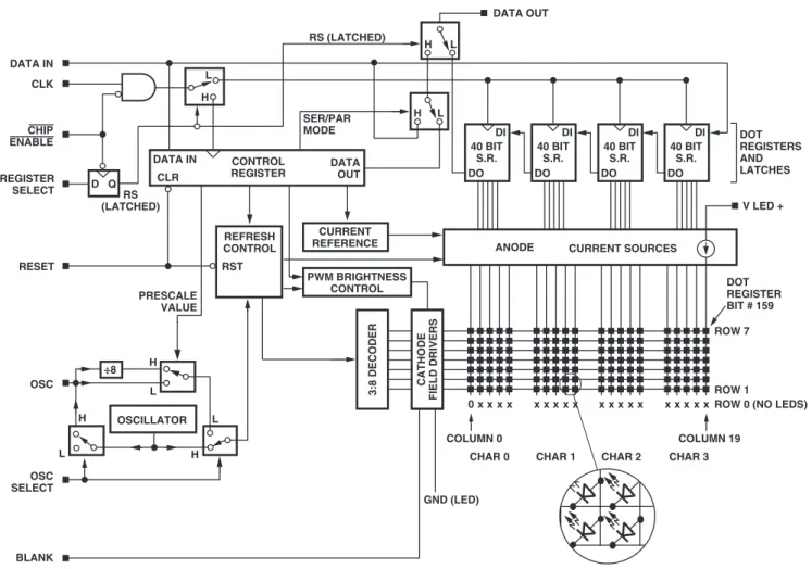
Display Overview
The HCMS-39XX series is a family of LED displays driven by on-board CMOS ICs. The LEDs are configured as 5x7 font characters and are driven in groups of 4 characters per IC. Each IC consists of a 160-bit shift register (the Dot Register), two 7-bit Control Words, and refresh circuitry. The Dot Register contents are mapped on a one-to-one basis to the display. Thus, an individual Dot Register bit uniquely controls a single LED.
Eight-character displays have two ICs that are cascaded. The Data Out line of the first IC is internally connected to the Data In line of the second IC forming a 320-bit Dot Register. The display’s other control and power lines are connected directly to both ICs.
Reset
Reset initializes the Control Registers (sets all Control Register bits to logic low) and places the display in the sleep mode. The Reset pin should be connected to the system power on reset circuit. The Dot Registers are not cleared upon power-on or by Reset. After power-on, the Dot Register contents are random; however, Reset will put the display in sleep mode, thereby blanking the LEDs. The Control Register and the Control Words are cleared to all zeros by Reset.
To operate the display after being Reset, load the Dot Register with logic lows. Then load Control Word 0 with the desired brightness level and set the sleep mode bit to
logic high.
Dot Register
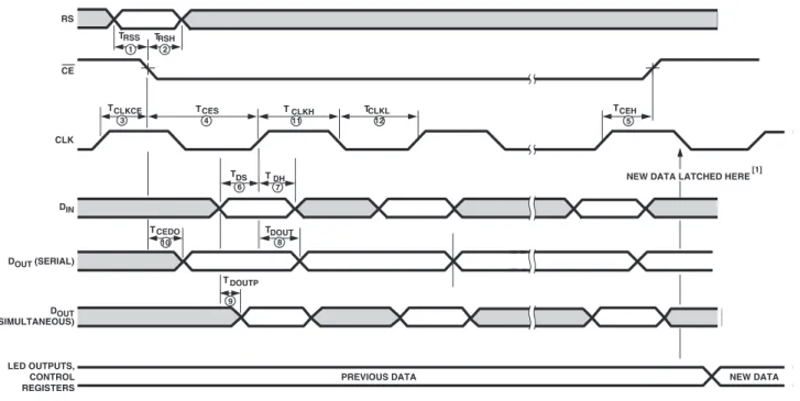
The Dot Register holds the pattern to be displayed by the LEDs. Data is loaded into the Dot Register according to the procedure shown in Table 1 and Figure 5.
First RS is brought low, then CE is brought low. Next, each successive rising CLK edge will shift in the data at the DIN pin. Loading a logic high will turn the corresponding LED on; a logic low turns the LED off. When all 160 bits have been loaded (or 320 bits in an 8-digit display), CE is brought to logic high.
When CLK is next brought to logic low, new data is latched into the display dot drivers. Loading data into the Dot Register takes place while the previous data is displayed and eliminates the need to blank the display while loading data.
Table 1. Register Truth Table
Function CLK CE RS
Select Dot Register Not Rising ↓ L
Load Dot Register DIN = HIGH LED = “ON” DIN = LOW LED = “OFF”
↑ L X
Copy Data from Dot Register to Dot Latch L H X
Select Control Register Not Rising ↓ H
Load Control Register [1,3] ↑ L X
Latch Data to Control Word [2] L H X
Notes:
1. BIT D0 of Control Word 1 must have been previously set to Low for serial mode or High for simultaneous mode.
2. Selection of Control Word 1 or Control Word 0 is set by D7 of the Control Shift Register. The unselected control word retains its previous value. 3. Control Word data is loaded Most Significant Bit (D7) first.
Figure 5. HCMS-39XX write cycle timing diagram.
Pixel Map
In a 4-character display, the 160- bits are arranged as 20 columns by 8 rows. This array can be conceptualized as four 5 x 8 dot matrix character locations, but only 7 of the 8 rows have LEDs (see Figures 6 & 7). The bottom row (row 0) is not used. Thus, latch location 0 is never displayed. Column 0 controls the left-most column. Data from Dot Latch locations 0-7 determine whether or not pixels in Column 0 are turned-on or turned-off. Therefore, the
NOTE:
1. DATA IS COPIED TO THE CONTROL REGISTER OR THE DOT LATCH AND LED OUTPUTS WHEN CE IS HIGH AND CLK IS LOW. TRSS TRSH
TCLKCE TCES TCLKH TCLKL TCEH
DS T TDH CEDO T TDOUT DOUTP T
PREVIOUS DATA NEW DATA
NEW DATA LATCHED HERE[1] CE RS CLK DIN LED OUTPUTS, CONTROL REGISTERS DOUT (SIMULTANEOUS) DOUT (SERIAL) 3 4 1 2 5 12 11 6 7 10 8 9
lower left pixel is turned-on when a logic high is stored in Dot Latch location 1. Characters are loaded in serially, with the left-most character being loaded first and the rightmost character being loaded last. By loading one character at a time and latching the data before loading the next character, the figures will appear to scroll from right to left.
Figure 6. Block diagram for HCMS-39xx. 40 BIT S.R. DO DI DATA IN OSCILLATOR ÷8 CLK CHIP ENABLE REGISTER SELECT RESET OSC OSC SELECT BLANK DATA IN CLR DATA OUT CONTROL REGISTER REFRESH CONTROL RST PRESCALE VALUE H L H L L H D Q RS (LATCHED) L H CURRENT REFERENCE PWM BRIGHTNESS CONTROL L H L H RS (LATCHED) SER/PAR MODE 3:8 DECODER 40 BIT S.R. DO DI 40 BIT S.R. DO DI 40 BIT S.R. DO DI
ANODE CURRENT SOURCES
V LED +
GND (LED) 0
CHAR 0
COLUMN 0 COLUMN 19
CHAR 1 CHAR 2 CHAR 3 ROW 7
DOT REGISTER BIT # 159
ROW 1
ROW 0 (NO LEDS) DOT REGISTERS AND LATCHES DATA OUT CATHODE FIELD DRIVERS x x x x x x x x x x x x x x x x x x x
Figure 7. Pixel map
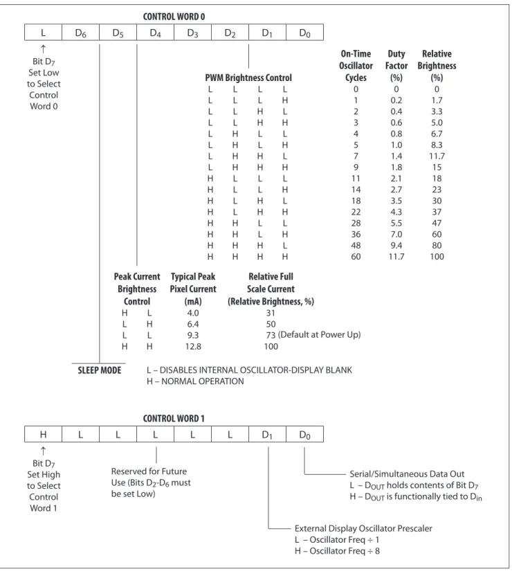
Control Register
The Control Register allows software modification of the IC’s operation and consists of two independent 7-bit control words. Bit D7 in the shift register selects one of the two 7-bit control words. Control Word 0 performs pulse width modulation Figure 7. Pixel map. brightness control, peak pixel current brightness control, and sleep mode. Control Word 1 sets serial/simultaneous data out mode, and external oscillator prescaler. Each function is indepen-dent of the others.
Control Register Data Loading
Data is loaded into the Control Register, MSB first, according to the procedure shown in Table 1 and Figure 5. First, RS is brought to logic high and then CE is brought to logic low. Next, each successive rising CLK edge will shift in the data on the DIN pin. Finally, when 8 bits have been loaded, the CE line is brought to logic high. When CLK goes to logic low, new data is copied into the selected control word. Loading data into the Control Register takes place while the previous control word configures the display.
Control Word 0
Loading the Control Register with D7 = Logic low selects
Control Word 0 (see Table 2). Bits D0-D3 adjust the
display brightness by pulse width modulating the LED on time, while Bits D4-D5 adjusts the display brightness
by changing the peak pixel current. Bit D6 selects normal
operation or sleep mode.
Sleep mode (Control Word 0, bit D6 = Low) turns off the
Internal Display Oscillator and the LED pixel drivers. This mode is used when the IC needs to be powered up, but does not need to be active. Current draw in sleep mode is nearly zero. Data in the Dot Register and Control Words are retained during sleep mode.
Control Word 1
Loading the Control Register with D7 = logic high selects
Control Word 1. This Control Word performs two functions: serial/ simultaneous data out mode and external oscillator prescale select (see Table 2).
ROW 0 (NOT USED) DATA TO NEXT CHARACTER PIXEL DATA FROM PREVIOUS CHARACTER ROW 7 ROW 6 ROW 5 ROW 4 ROW 3 ROW 2 ROW 1
Table 2. Control Shift Register. CONTROL WORD 0 L D6 D5 D4 D3 D2 D1 D0 ↑ Bit D7 Set Low to Select Control Word 0
On-Time Duty Relative Oscillator Factor Brightness
Cycles (%) (%) 0 0 0 1 0.2 1.7 2 0.4 3.3 3 0.6 5.0 4 0.8 6.7 5 1.0 8.3 7 1.4 11.7 9 1.8 15 11 2.1 18 14 2.7 23 18 3.5 30 22 4.3 37 28 5.5 47 36 7.0 60 48 9.4 80 60 11.7 100 PWM Brightness Control L L L L L L L H L L H L L L H H L H L L L H L H L H H L L H H H H L L L H L L H H L H L H L H H H H L L H H L H H H H L H H H H SLEEP MODE Peak Current Brightness Control Typical Peak Pixel Current (mA) Relative Full Scale Current (Relative Brightness, %) H L 4.0 31 L H 6.4 50 L L 9.3 73 H H 12.8 100
L – DISABLES INTERNAL OSCILLATOR-DISPLAY BLANK H – NORMAL OPERATION
(Default at Power Up)
Reserved for Future Use (Bits D2-D6 must be set Low)
Serial/Simultaneous Data Out L – DOUT holds contents of Bit D7 H – DOUT is functionally tied to Din External Display Oscillator Prescaler
L – Oscillator Freq ÷ 1 H – Oscillator Freq ÷ 8 CONTROL WORD 1 H L L L L L D1 D0 ↑ Bit D7 Set High to Select Control Word 1
Serial/Simultaneous Data Output D0
Bit D0 of control word 1 is used to switch the mode of
DOUT between serial and simultaneous data entry during
Control Register writes. The default mode (logic low) is the serial DOUT mode. In serial mode, DOUT is connected to the
last bit (D7) of the Control Shift Register.
Storing logic high to bit D0 changes DOUT to simultaneous
mode, which affects the Control Register only. In simul-taneous mode, DOUT is logically connected to DIN. This
arrangement allows multiple ICs to have their Control Registers written to simultaneously. For example, for n ICs in the serial mode, n * 8 clock pulses are needed to load the same data in all Control Registers. In the simultaneous mode, n ICs only need 8 clock pulses to load the same data in all Control Registers. The propagation delay from the first IC to the last is n * tDOUTP.
External Oscillator Prescaler Bit D1
Bit D1 of Control Word 1 is used to scale the frequency of
an external Display Oscillator. When this bit is logic low, the external Display Oscillator directly sets the internal display clock rate. When this bit is logic high, the external oscillator is divided by 8. This scaled frequency then sets the internal display clock rate. It takes 512 cycles of the display clock (or 8 x 512 = 4096 cycles of an external clock with the divide by 8 prescaler) to completely refresh the display once. Using the prescaler bit allows the designer to use a higher external oscillator frequency without extra circuitry.
This bit has no affect on the internal Display Oscillator Frequency.
Bits D2-D6
These bits must always be programmed to logic low.
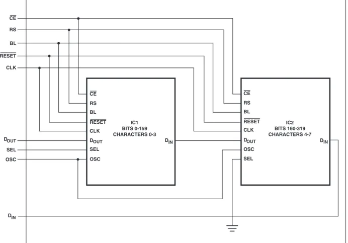
Cascaded ICs
Figure 8 shows how two ICs are connected within an HCMS-39XX display. The first IC controls the four left-most characters and the second IC controls the four rightmost characters. The Dot Registers are connected in series to form a 320-bit dot shift register. The location of pixel 0 has not changed. However, Dot Shift Register bit 0 of IC2 becomes bit 160 of the 320-bit dot shift register.
The Control Registers of the two ICs are independent of each other. This means that to adjust the display bright-ness the same control word must be entered into both ICs, unless the Control Registers are set to simultaneous mode.
Longer character string systems can be built by cascading multiple displays together. This is accomplished by creating a fiveline bus. This bus consists of CE, RS, BL, Reset, and CLK. The display pins are connected to the cor-responding bus line. Thus, all CE pins are connected to the CE bus line. Similarly, bus lines for RS, BL, Reset, and CLK are created. Then DIN is connected to the right-most
display. DOUT from this display is connected to the next
display. The left-most display receives its DIN from the
DOUT of the display to its right. DOUT from the left-most
display is not used.
Each display may be set to use its internal oscillator, or the displays may be synchronized by setting up one display as the master and the others as slaves. The slaves are set to receive their oscillator input from the master’s oscillator output.
Figure 8. Cascaded ICs. CE IC2 BITS 160-319 CHARACTERS 4-7 RS BL SEL OSC CLK DOUT DIN IC1 BITS 0-159 CHARACTERS 0-3 DIN RS BL SEL OSC CLK DOUT CE RESET RESET RS BL SEL OSC CLK DOUT CE RESET DIN
Figure 9. Maximum power dissipation per IC versus ambient temperature.
Appendix A. Thermal Considerations
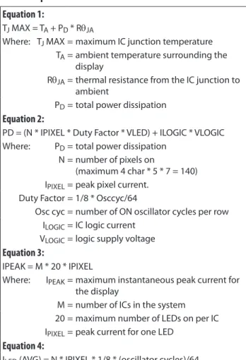
The display IC has a maximum junction temperature of 150° C. The IC junction temperature can be calculated with Equation 1 in Table 3.
A typical value for RθJA is 100°C/ W. This value is typical for
a display mounted in a socket and covered with a plastic filter. The socket is soldered to a 0.062 inch thick PCB with 0.020-inch wide, Figure 9. Maximum power dissipation per IC versus ambient temperature. one ounce copper traces. PD can be calculated as Equation 2 in Table 3.
Figure 9 shows how to derate the power of one IC versus ambient temperature. Operation at high ambient tem-peratures may require the power per IC to be reduced. The power consumption can be reduced by changing the N, IPIXEL, Osc cyc or VLED. Changing VLOGIC has very little
impact on the power consumption.
0 25 0.7 0.6 0.5 0.4 0.3 0.2 0.1 60 55 50 45 40 35 30 0.8 0.9 1.0 1.1 1.2 85 80 75 70 65 90 1.3 PD MAX – MAXIMUM POWER DISSIPATION PER IC – W
TA – AMBIENT TEMPERATURE – °C
Appendix B. Electrical Considerations
Current Calculations
The peak and average display current requirements have a significant impact on power supply selection. The maximum peak current is calculated with Equation 3 in Table 3.
The average current required by the display can be calcu-lated with Equation 4 in Table 3.
The power supply has to be able to supply IPEAK transients
and supply ILED (AVG) continuously. The range on VLED
allows noise on this supply without signifi cantly changing the display brightness.
V
LOGICand V
LEDConsiderations
The display uses two independent electrical systems. One system is used to power the display’s logic and the other to power the display’s LEDs. These two systems keep the logic supply clean.
Separate electrical systems allow the voltage applied to VLED and VLOGIC to be varied in dependently. Thus, VLED
can vary from 0 to 5.5 V without affecting either the Dot or the Control Registers. VLED can be varied between 3.1 to
5.5 V without much noticeable variation in light output to the human eyes. There is also no pixel mismatch observed. The intensity of the light output takes a plunge if operated less than 3.1 V. There is also no pixel mismatch observed at voltage as low as 2.6 V. However, operating below 3.1 V is not recommended. Dimming the display by pulse width modulating VLED is also not recommended.
VLOGIC can vary from 3.0 to 5.5 V without affecting either
the displayed message or the display intensity. However, operating below 3 V may change the timing and logic levels and may cause Dot and Control Registers to be altered. Thus, operation of the display below 3.0 V is not recommended.
The logic ground is internally connected to the LED ground by a substrate diode. This diode becomes forward biased and conducts when the logic ground is 0.4 V greater than the LED ground. The LED ground and the logic ground should be connected to a common ground, which can withstand the current introduced by the switching LED drivers. When separate ground connections are used, the LED ground can vary from -0.3 V to +0.3 V with respect to the logic ground. Voltages below -0.3 V can cause all the dots to be ON. Voltage above +0.3 V can cause dimming and dot mismatch.
Using a decoupling capacitor between the power supply and ground will help prevent any supply noise in the frequency range greater than that of the functioning display from interfering with the display’s internal circuitry. The value of the capacitor depends on the series resistance from the ground back to the power supply and the range of frequencies that need to be suppressed. It is also advan-tageous to use the largest ground plane possible.
Electrostatic Discharge
The inputs to the ICs are protected against static discharge and input current latch up. However, for best results, standard CMOS handling precautions should be used. Before use, the HCMS-39XX should be stored in antistatic tubes or in conductive material. During assembly, a grounded conductive work area should be used and assembly personnel should wear conduc-tive wrist straps. Lab coats made of synthetic material should be avoided since they are prone to static buildup. Input current latch up is caused when the CMOS inputs are subjected to either a voltage below ground (VIN < ground) or to a voltage higher than
VLOGIC (VIN > VLOGIC) and when a high current is forced
into the input. To prevent input current latch up and ESD damage, unused inputs should be connected to either ground or VLOGIC. Voltages should not be applied to the
inputs until VLOGIC has been applied to the display.
Table 3. Equations.
Equation 1:
TJ MAX = TA + PD * RθJA
Where: TJ MAX = maximum IC junction temperature TA= ambient temperature surrounding the
display
RθJA= thermal resistance from the IC junction to ambient
PD= total power dissipation
Equation 2:
PD = (N * IPIXEL * Duty Factor * VLED) + ILOGIC * VLOGIC
Where: PD= total power dissipation
N = number of pixels on
(maximum 4 char * 5 * 7 = 140) IPIXEL= peak pixel current.
Duty Factor = 1/8 * Osccyc/64
Osc cyc = number of ON oscillator cycles per row ILOGIC= IC logic current
VLOGIC= logic supply voltage
Equation 3:
IPEAK = M * 20 * IPIXEL
Where: IPEAK= maximum instantaneous peak current for the display
M = number of ICs in the system 20 = maximum number of LEDs on per IC IPIXEL= peak current for one LED
Equation 4:
ILED (AVG) = N * IPIXEL * 1/8 * (oscillator cycles)/64 (See Variable Definitions above)
For product information and a complete list of distributors, please go to our web site: www.avagotech.com
Avago, Avago Technologies, and the A logo are trademarks of Avago Technologies in the United States and other countries. Data subject to change. Copyright © 2005-2012 Avago Technologies. All rights reserved. Obsoletes 5988-7528EN AV02-3679EN - June 25, 2012
Appendix C. Oscillator
The oscillator provides the internal refresh circuitry with a signal that is used to synchronize the columns and rows. This ensures that the right data is in the dot drivers for that row. This signal can be supplied from either an external source or the internal source.
A display refresh rate of 100 Hz or faster ensures flicker- free operation. Thus, for an external oscillator the frequency should be greater than or equal to 512 x 100 Hz = 51.2 kHz. Operation above 1 MHz without the prescaler or 8 MHz with the prescaler may cause noticeable pixel-to-pixel mismatch.
Appendix D. Refresh Circuitry
This display driver consists of 20 one-of-eight column decoders and 20 constant current sources, 1 one-of-eight row decoder and eight row sinks, a pulse width modu-lation control block, a peak current control block, and the circuit to refresh the LEDs. The refresh counters and oscillator are used to synchronize the columns and rows. The 160 bits are organized as 20 columns by 8 rows. The IC illuminates the display by sequentially turning ON each of the 8 row-drivers. To refresh the display once takes 512 oscillator cycles. Because there are eight row drivers, each row driver is selected for 64 (512/8) oscillator cycles. Four cycles are used to briefly blank the display before the following row is switched on. Thus, each row is ON for 60 oscillator cycles out of a possible 64. This corresponds to the maximum LED on time.
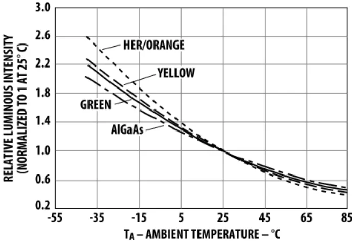
The temperature of the display will also affect the LED brightness as shown in Figure 10.
Appendix E. Display Brightness
Two ways have been shown to control the brightness of this LED display: setting the peak current and setting the duty factor. Both values are set in Control Word 0. To compute the resulting display brightness when both PWM and peak current control are used, simply multiply the two relative brightness factors. For example, if Control Register 0 holds the word 1001101, the peak current is 73% of full scale (BIT D5 = L, BIT D4 = L) and the PWM is
set to 60% duty factor (BIT D3 = H, BIT D2 = H, BIT D1 = L,
BIT D0 = H). The resulting brightness is 44% (0.73 x 0.60 =
0.44) of full scale.
The temperature of the display will also affect the LED brightness as shown in Figure 10.
Appendix F. Reference Material
Application Note 1027: Soldering LED Components Application Note 1015: Contrast Enhancement Techniques for LED Displays
Figure 10. Relative luminous Intensity versus ambient temperature.
YELLOW HER/ORANGE GREEN AlGaAs -55 -35 -15 5 25 45 65 85 0.2 3.0 2.6 2.2 1.8 1.4 1.0 0.6 TA – AMBIENT TEMPERATURE – °C RELATIVE LUMINOUS INTENSITY (NORMALIZED TO 1 AT 25° C)