International Journal of Emerging Technology and Advanced Engineering
Website: www.ijetae.com (ISSN 2250-2459, ISO 9001:2008 Certified Journal, Volume 7, Issue 11, November 2017)
324
Crosstalk and Delay Analysis of a CMOS-Gate Driven Coupled
Interconnects in Sub-threshold Conduction
Bhattu. Hari Prasad Naik
1, Chandra Sekhar Paidimarry
21,2Dept. Of ECE, University College of Engineering, Osmania University, Hyderabad, India.
Abstract—Advancements in technology have resulted in high speed and complex VLSI interconnects. Accurate analysis of these high frequency interconnects in time/frequency domain is very essential along with crosstalk noise estimation. The demand for ultra low power circuit designs in deep sub-micron is increasing so as to achieve low power efficient designs. This work employs Sub-threshold conduction method for estimation of crosstalk noise. Here, analysis of propagation delays and crosstalk noise in a coupled RLC interconnects is performed in Sub-threshold conduction is proposed. In Sub-threshold regime i.e. VGS<Vth
and Vdd<Vth circuit design consume low power for the active
operations and simultaneously dissipate low leakages than their alternatives i.e. strong inversion but with increased delays. Coupling between interconnects can causes serious effects on the performances such as high propagation delays, power dissipations and can induce over/under shoot in to the signal. So, it is essential to predict interconnects coupling noise as it may create logical errors. Interconnects are driven by CMOS buffer and the buffer operates in Sub-threshold regime. The crosstalk analysis simulation is performed in strong inversion as well as in Sub-threshold with 180nm, 130nm and 50nm technology nodes. The simulation results have validated that crosstalk noise voltage obtained in Sub-threshold is stable and lower than its counterpart. But the propagation delays have increased.
Keywords—Delays, Sub-threshold, Crosstalk, Weak Inversion, Signal Integrity, Interconnects, Far End Crosstalk.
I. INTRODUCTION
With the technology advancements in the deep-submicron (DSM) regime, feature size of the MOS transistor and interconnects are scaled down at significant rate. These large IC chips have necessitated to use very long interconnects [1]. These interconnects connects various components on a chip and distribute power, ground, high speed clocks, data and control signals. Interconnect parasitic capacitance also presents loading effect to CMOS circuits, thereby increasing the propagation delays and excess power dissipation. High supply voltage or near threshold voltage leads to high power dissipation. Reduction in power consumption makes the designs lighter, reduces cooling subsystems and extends the life of energy source as well.
Hence, it is necessary to minimize power dissipation without large leakage currents and delay penalties in the designs. In deep-submicron region (<0.18um), weak inversion or Sub-threshold conduction of the device greatly exhibit the potential of satisfying the demands of ultra low power [20] systems. These applications require very low operating clock frequency (eg. Hearing aids). Sub-threshold conduction uses supply voltage less than that of threshold voltage (VGS<Vth) of the transistor. So, driving a CMOS circuits with Sub-threshold or weak current (I0) can reduce the overall power dissipation than the dissipation of power in the strong inversion region. Therefore, Sub-threshold logics can emerge as an approach in designing the power efficient circuits that consumes low power and dissipates low leakages. Sub-threshold current (I0) is lower in magnitude (uW) than the drain saturation (IDS) current magnitude (mW) in strong inversion region i.e. IDS>>I0. The driving Sub-threshold current may limit the performances but the power usage is greatly minimized which extends the life of a source. Interconnects on a IC chip plays a vital role in determining the propagation of signal, signal integrity[11], [19] and power consumption in the design. With technology, device scaling has greatly reduced the spacing between interconnects. This spacing in-turn has increased the coupling between interconnects. Coupling is the main source of coupling noise and is commonly referred as Crosstalk. In-terms of design performance metrics, crosstalk [13] is an unwanted and must be kept as low (≈50mV) as possible. Crosstalk can cause serious effects such as high propagation delays, excess power dissipation and can induce over and undershoot in to the signal and generates false switching in the circuit.
International Journal of Emerging Technology and Advanced Engineering
Website: www.ijetae.com (ISSN 2250-2459, ISO 9001:2008 Certified Journal, Volume 7, Issue 11, November 2017)
325 In this approach, RLC coupled interconnects are driven by a non-linear CMOS driver operating in strong inversion region with VGS>Vth and Vdd>Vth condition. Objective of this work is to analyze the crosstalk noise between the coupled RLC interconnects driven by a CMOS buffer operating in Sub-threshold conduction and estimate the propagation delays [9], [16]. Objective of this work is to analyze the crosstalk noise voltage between the coupled RLC interconnects. Interconnects are driven by a CMOS buffer operating in strong inversion and Sub-threshold conduction. Simultaneously, obtain the propagation delays as well.
II. SUB-THRESHOLD CONDUCTION MODEL
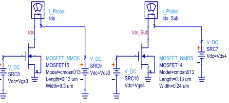
[image:2.612.326.564.300.411.2]The circuit designs which are operating in Sub-threshold regime can provide minimum energy with strong energy constraints. When VGS=Vth, current flowing through the MOS device does not drop abruptly. The device is partially conducting because of the diffusion current referred as threshold or weak current. Figure.1 illustrates the Sub-threshold conduction analysis of a NMOS transistor. For analysis, assume VGS<Vth and Vdd<Vth to ensure the Sub-threshold current along the device. In Sub-Sub-threshold regime channel of the NMOS transistor is not inverted but the current flows only by diffusion.
Fig. 1. Sub-threshold conduction current of NMOS transistor.
When VGS<Vth, Sub-threshold current (I0) is a leakage current due to diffusion and decays exponentially. The leakage current in the Sub-threshold region is approximated as in equation (1).
T DS T DS th GS Sub D V V V V V V I
I 0*exp 1 exp (1)
T th GS Sub DV
V
V
I
I
exp
*
0 (2)
Sub-threshold slope factor
ox d C C 1 ,
Thermal Voltage
q KT
VT ,
T DS V V exp 1
roll-off current ID when VDS Vth
[image:2.612.54.289.441.547.2]In Sub-threshold conduction, it is assumed that total drain current (ID) equals Sub-threshold current (I0). From (2), ID varies exponentially with VGS. Threshold voltage point (Vth) of a transistor is defined as point where current (ID) starts rising exponentially w.r.t VGS and is shown in Figure.2.
Fig. 2. Threshold Voltage point (Vth) of NMOS w.r.t VGS.
Typically, when VGS<Vth current drops as fast as possible. The rate at which current (I0) declines when VGS<Vth is a measure of quality of the device known as Sub-threshold slope (S) and is given by equation (3) as:
) 10 ln( q KT S (3)
The slope factor predicts by how much value VGS needs to be reduced for reduction in drain current magnitude (mV/decade). The value of S gives the inverse of the slope of current ID Vs VGS in mill volts/decade. The ideal value of S at room temperature is S=60mV/decade which occurs at the n=1. Substituting (3) in (1) gives the Sub-threshold drain ID-Sub.
T DS DS th GS Sub D V V S V V V I
I 1 exp
) 10 ln( / exp * 0 T DS V V V Sub D V V I
I *10 GS th DS 1 exp 0
International Journal of Emerging Technology and Advanced Engineering
Website: www.ijetae.com (ISSN 2250-2459, ISO 9001:2008 Certified Journal, Volume 7, Issue 11, November 2017)
[image:3.612.49.288.122.277.2]326 Fig. 3. NMOS Characteristic of ID vs VDS in 130nm.
Figure.3 shows the characteristics plot between ID and VDS for different values of VGS in 130nm. NMOS transistor operated in strong inversion region with VGS>Vth the drain current is in uA. Similarly, when the NMOS is operated in sub-threshold/weak inversion VGS<Vth and Vdd<Vth sub-threshold current is in nA.
III. CMOS GATE IN SUB-THRESHOLD REGION
[image:3.612.323.569.141.297.2]The previous works of [3], the interconnect driver is modeled with a linear resistor. But, in many practical cases a non-linear [4] and [5] buffers are used as drivers operating in strong inversion region. Figure.4 shows the comparison of CMOS gate model operating in strong inversion (VGS>Vth) and Sub-threshold conduction (VGS<Vth and Vdd<Vth) region.
Fig. 4. CMOS Driver Model Characteristics.
The VTC characteristics of the CMOS driver in 180nm, 130nm and 50nm scaled technology is shown in Figure.5. The characteristics show that driver can also be operated in Sub-threshold [18] conduction region so as to achieve low power.
Fig. 5. VT-Characteristics of CMOS Driver in 180nm, 130nm, 50nm.
IV. FUNCTIONAL CROSSTALK ANALYSIS IN COUPLED RLC INTERCONNECTS
In any circuit design, crosstalk is an unwanted metric and can causes serious effects on the performances such as high propagation delays, power dissipations and can induce over/under shoot in to the signal. So, it is necessary to predict interconnects crosstalk noise voltage. Here, propagation delay and analysis of crosstalk in strong inversion and sub-threshold is performed.
A. Crosstalk with CMOS- Gate in Strong Inversion
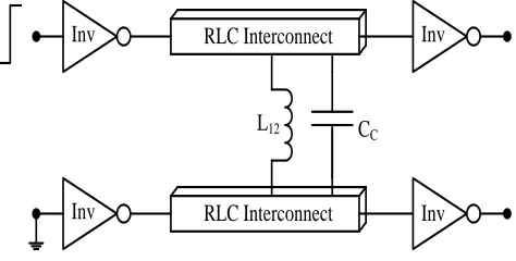
Often, interconnects on a chip are treated as transmission lines [11]. These are driven by a CMOS buffer [4], [6] and [7] as shown in Figure.6. The two interconnects are coupled through inductive and capacitive coupling which is the major source of crosstalk noise voltage.
RLC Interconnect
RLC Interconnect
L
12C
CInv
Inv
[image:3.612.50.289.462.615.2]Inv
Inv
[image:3.612.326.563.519.639.2]International Journal of Emerging Technology and Advanced Engineering
Website: www.ijetae.com (ISSN 2250-2459, ISO 9001:2008 Certified Journal, Volume 7, Issue 11, November 2017)
327 Here the CMOS inverter is operated in cut-off, linear or ohmic and saturation regions known as ―Strong Inversion operation‖. When VGS>Vth, VDS>VGS-Vth the transistor turns-ON and the drain current (IDS) is given by equation (20):
Linear
Saturation V
V L W C
V V V V L W C
off Cut I
th GS ox
DS DS th GS ox
DS
2 0
2
0
2
2 0
[image:4.612.48.287.197.659.2]
(20)
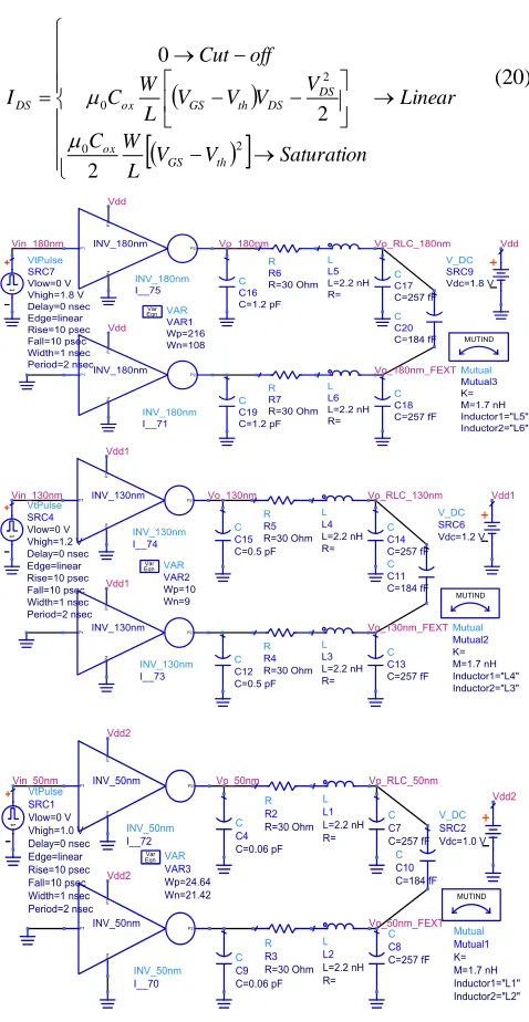
Fig. 7. Crosstalk Analysis of Coupled RLC with CMOS Driver Operating in Strong Inversion region.
[image:4.612.338.559.211.377.2]Figure.7 shows the model of coupled RLC [12], [16] interconnects that are driven by a CMOS drivers operating in the strong inversion region. The crosstalk noise [6], [9] analysis is performed for different CMOS scaled technologies i.e. 180nm, 130nm and 50nm respectively.
Fig. 8. Crosstalk Voltage (FEXT) of Coupled Interconnects.
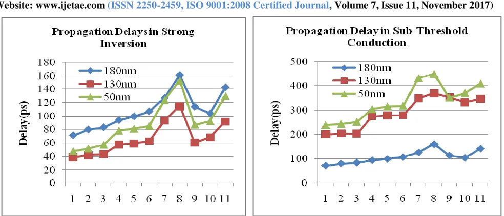
The crosstalk noise voltage in coupled RLC interconnect is measured with different CMOS driver strengths and is tabulated in Table-1. The crosstalk noise response is shown in Figure.8. It shows that crosstalk noise decreases with respect to technology scaling and is low in 50nm. Propagation delay through the interconnect increases.
B. Crosstalk with Gate in Sub-threshold Conduction
International Journal of Emerging Technology and Advanced Engineering
Website: www.ijetae.com (ISSN 2250-2459, ISO 9001:2008 Certified Journal, Volume 7, Issue 11, November 2017)
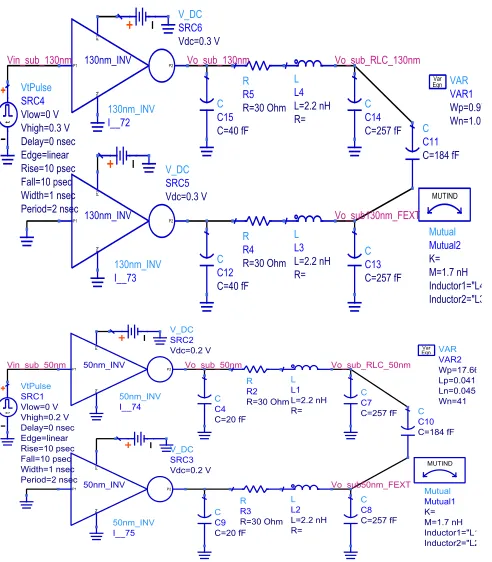
[image:5.612.50.296.137.418.2]328 Fig. 9. Crosstalk Analysis of Coupled Interconnect with CMOS Gate
in Sub-threshold Conduction.
The crosstalk voltage response of coupled RLC interconnects in Sub-threshold conduction is shown in Figure.10.
[image:5.612.324.562.217.338.2]Crosstalk voltage magnitude is in the range of ≈35mV (50nm) and ≈70mV (130nm) respectively. Transient analysis is performed for a period of 5ns with pulse as input and signal rise/fall time tr=tf=10ps and pulse width of 2ns. Crosstalk noise voltages and propagation delays are tabulated in Table I.
Fig. 10.Transient Analysis of Coupled RLC Interconnect.
International Journal of Emerging Technology and Advanced Engineering
Website: www.ijetae.com (ISSN 2250-2459, ISO 9001:2008 Certified Journal, Volume 7, Issue 11, November 2017)
329 TABLE 1
COMPARISON OF PROPAGATION DELAYS AND CROSSTALK NOISE IN STRONG INVERSION AND SUB-THRESHOLD REGION.
Coupled RLC Interconnect Parameters
Propagation Delays and Crosstalk Noise in Strong Inversion region
Delays and Crosstalk Noise in Sub-threshold/Weak Inversion
R (Ω)
L (nH)
C (fF)
Cc (fF)
M (nH)
tpd (ps)
Crosstalk 180nm [2],[7]
tpd (ps)
Crosstalk 130nm
tpd (ps)
Crosstalk 50nm
tpd (ps)
Crosstalk 130nm
tpd (ps)
Crosstalk 50nm 30 2.2 257 184 1.7 71.3 0.386 38.5 0.283 47.5 0.151 200 0.069 239 0.030
60 2.2 257 184 1.7 79.9 0.300 41.6 0.213 51.6 0.146 204 0.070 244 0.034
90 2.2 257 184 1.7 83.2 0.281 43.1 0.196 57.2 0.131 203 0.070 252 0.036
30 3.8 416 320 3.0 93.9 0.515 57.5 0.369 78.4 0.294 275 0.068 305 0.036
60 3.8 416 320 3.0 99.5 0.403 59.2 0.276 81.3 0.254 278 0.067 316 0.038
90 3.8 416 320 3.0 107 0.361 62.4 0.303 85.2 0.234 279 0.068 319 0.040
58 4.1 884 633 3.2 127 0.397 93.3 0.264 124 0.294 349 0.049 432 0.035
72 5.1 1100 788 4.0 161 0.385 115 0.257 153 0.296 370 0.041 449 0.035
82 3.3 520 372 2.6 114 0.347 60.4 0.238 87.0 0.231 354 0.062 352 0.037
56 3.2 590 422 2.5 104 0.381 68.3 0.260 92.7 0.251 332 0.060 371 0.035
109 4.4 700 501 3.5 143 0.347 91.9 0.235 130 0.246 347 0.057 409 0.037
International Journal of Emerging Technology and Advanced Engineering
Website: www.ijetae.com (ISSN 2250-2459, ISO 9001:2008 Certified Journal, Volume 7, Issue 11, November 2017)
[image:7.612.68.560.124.335.2]330
Fig. 11.Transient Analysis of Coupled RLC Interconnect.
V. CONCLUSION
In this paper, an approach for crosstalk noise voltage estimation of a coupled RLC interconnects is proposed. Strong Inversion and Sub-threshold conduction logics are used in the crosstalk analysis. Sub-threshold conduction uses low VGS, Vdd to achieve low power dissipation. In Sub-threshold region, current is a weak current of low in magnitude (nA). Crosstalk analysis of coupled RLC interconnects driven by a non-linear CMOS buffer operating in strong and weak inversion is evaluated. The simulation results have validated that the crosstalk noise is low and stable in sub-threshold than its counterpart i.e. strong inversion. Simulation is performed with different scaled technology nodes 180nm, 130nm and 50nm respectively. Crosstalk noise is minimized to great extent but propagation delays have increased because of scaling. Hence, Sub-threshold logic designs can be used as an alternative to strong inversion to achieve low power efficient circuits.
REFERENCES
[1] Semiconductor Industry Association, International Technology Roadmap for Semiconductors (ITRS), 2011.
[2] P.Chandra Sekhar, B.Pradeep Kumar, K.Srinivas, ―A Novel Approach to Crosstalk Noise Analysis in CMOS Inverter Driven Coupled RLC Interconnects,‖IEEE Conf. INDICON, 2013. [3] K. Agarwal, D. Sylvester, and D. Blaauw, ―Modeling and analysis of
crosstalk noise in coupled RLC interconnects,‖ IEEE Trans. Comput.Aided Design Integr. Circuits Syst., vol. 25, no. 5, pp. 892– 901, May 2006.
[4] B. K.KaushikandS.Sarkar,―CrosstalkanalysisforaCMOS-gate-driven coupled interconnects,‖ IEEE Trans. Comput.-Aided Design Integr. Circuits Syst., vol. 27, no. 6, pp. 1150–1154, Jun. 2008.
[5] B. K. Kaushik, S. Sarkar, R. P. Agarwal, and R. C. Joshi, ―An analytical approach to dynamic crosstalk in coupled
[6] interconnects,‖ Microelectron. J., vol. 41, pp. 85–92, Feb. 2010. [7] V. Ramesh Kumar, B. K. Kaushik, and A. Patnaik, ―Dynamic
crosstalk analysis of CMOS driven RLC interconnects using FDTD method,‖ in Proc. IEEE Conf. AP-S /USNC-URSI, Jul. 7–13, 2013, p. 80.
[8] V. Ramesh Kumar, B. K. Kaushik, and A. Patnaik, ―An Accurate FDTD Model for Crosstalk Analysis of CMOS-Gate Driven Coupled RLC Interconnects,‖ in Proc. IEEE Trans., Oct. 7–13, 2014 [9] Md. Maniruzzaman, Shakil Ahmed, Galib Md. Fattah, Rafia Nishat
Toma, ―Estimation of crosstalk noise for RLC interconnects in deep submicron VLSI circuit,‖May. 2015.
[10]Sourajeet Roy, Anestis Dounavis, ―Efficient Delay and Crosstalk Modeling of RLC Interconnects Using Delay Algebraic Equations‖. IEEE Trans.on Very Large Scale Integration Systems Vol.19, no.2, pp. 342-346, Feb.2011.
[11]Vikas Maheshwari, Abhishek Sharma, R.Kar, ―Transient and Delay Analysis for On-Chip High Speed VLSI RLCG Global Interconnect for Unit Impulse Input,‖ IEEE Conf. Malaysia, Dec. 2011.
[12]Do-Won Kim , Chao Li & Patrick Lo Guo Qiang, ―Signal integrity and crosstalk analysis of the transmission lines on SOI substrate for high-speed up to 50 GHz,‖ IEEE 18th Electronics Packaging Technology Conference (EPTC), Singapore, Dec. 2016 .
[13]A.B.Khang, S.Muddu, ―An Analytical Delay Model for RLC Interconnects,‖ IEEE Trans. on Computer Aided Design of Integrated Circuits Systems, pp.1507-1514, 1997.
International Journal of Emerging Technology and Advanced Engineering
Website: www.ijetae.com (ISSN 2250-2459, ISO 9001:2008 Certified Journal, Volume 7, Issue 11, November 2017)
331 [15]Rajib Kar, V. Maheshwari, Md. Maqbool, A. K. Mal, A. K.
Bhattacharjee, ―A Closed Form Modelling of Cross-talk for Distributed RLCG On-Chip Interconnects using Difference Model Approach‖. International Journal on Communication Technology.India, vol. 1, no. 1, .pp. 17-22, 2010.
[16]V.Maheshwari, Amar Baboo, Brajesh Kumar, Rajib Kar, D.Mandal & A. K. Bhattacharjee, ―Delay Model for VLSI RLCG Global Interconnects,‖ Asia Pacific Conference on Postgraduate Research in Microelectronics and Electronics (PrimeAsia). Hyderabad, India, Dec. 2012.
[17]Muhammad Sanaullah, Masud H. Chowdhury, ―Analysis of RLC Interconnect Delay Model using Second Order Approximation‖, IEEE Symposium Circuits and Systems (ISCAS), Melbourne VIC, Australia, Jun. 2014.
[18]Sunil Jadav, Rajeevan Chandel, Munish Vashishath, ―A Superior Delay Estimation Model for VLSI Interconnect in Current Mode Signaling‖, World Academy of Science Engineering and Technology, vol.9, no.2, 2015.
[19]Clayton R.Paul, ―Time Domain Analysis of Two Conductor Lines‖, pp.49-120, Wiley-IEEE Press, 2010.
[20]Eric Bogatin, ―Signal and Power Integrity Simplified‖, Prentice Hall, 2ndEdition, 2010.
[21]Stephan H.Hall, Garrett W. Hall, James A. McCall, ―High Speed Digital System Design: A Hand Book of Interconnect Theory and Design Practices‖, Wiley and Sons, 2000.
[22]Mike. Peng. Li, ―Jitter, Noise, and Signal Integrity at High-Speed‖, Westford, MAPrentice-Hall, 2008.
ABOUT AUTHORS:
Bhattu.HariPrasad Naik received B.Tech from Anurag Engineering College, JNTUH, and M.E degree in Digital System Engineering from University College of Engineering, Osmania University, Hyderabad, India in 2008. Currently, he is a Senior Research Fellow in Dept. of ECE, UCE, Osmania University, Hyderabad, Telangana. His areas of interests are crosstalk analysis, Electro-magnetics, signal integrity and power integrity in VLSI.
Email: [email protected]
Chandra Sekhar Paidimarry received B.E degree from Nagpur University, M.Tech degree from JNTU, Hyderabad and Ph.D from Osmania University in 1991, 1999 and 2009 respectively. He has been awarded with Post Doctoral Fellowship by Shizuoka University, Japan. He has been working in the Department of Electronics and Communication Engineering, University College of Engineering, Osmania University, Hyderabad from 2001.He has been elevated as Professor of ECE in 2015. His research interests include Computational Electro-magnetics, signal processing algorithms and VLSI Design Automation.