International Journal of Emerging Technology and Advanced Engineering
Website: www.ijetae.com (ISSN 2250-2459,ISO 9001:2008 Certified Journal, Volume 3, Issue 11, November 2013)
691
Novel Subthreshold and Gate Leakage Reduction Techniques
for 6T-SRAM Cell
V. S. V. Prabhakar
1, K. Lal Kishore
2 1Professsor, Deparment of ECE, GVP College of Engineering for Women, Vishakapatnam, India.
2Vice-Chancellor, JNTUA, Anantapur, India.
Abstract— Power has been an important issue for the present day microelectronic circuits of Soc designs. In the entire phase of design controlling power and dealing with power dissipation is very important. There are six leakage components in a MOS transistor. About 50 % of the total power consumption is through leakage components alone. Out of this 40 % power dissipation is through transistors.Out of them subthreshold leakage and gate leakage are of important concern for sub 100 nm devices. In this work we presented the main leakages in a 6T- SRAM cell. Later we presented an existing variable body biasing method and its performance. We proposed two novel methodologies HSVR, GSVE to reduce the subthreshold and gate leakage components. These methods are toplogy based leakage reduction methods applied for leakage reduction in the circuit level.We observed considerable reduction of both the components through the proposed methods.
Keywords—SRAM, Leakage, Gate Leakage,
subthresholdleakage
I. INTRODUCTION
Static RAM is a volatile type of semiconductor memory used to store data as long as power is on. SRAM (Fig 1) is widely used in latest designs to increase the speed of operations in Microprocessor and other computing areas. In the case of DRAM as the charge leaks and data is lost over a period of time, a refresh operation is required for every few milli seconds. But for SRAM, no such operation is required which is primary advantage of it.Embedded RAM’s with supply voltage of 0.6 V is reported in [1] through research and development of 16 MB DRAM have become prominent in present SoC technologies. In development of RAM’s we need to face challenges from four directions [2-4] to minimize the leakage current in the RAM cell.
a) Maintaining appropriate Signal voltage and Signal charge in the RAM cell.
b) Minimize the RAM cell area.
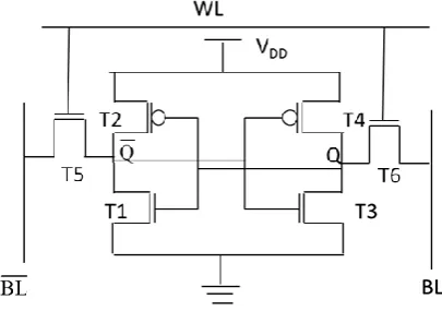
[image:1.595.332.535.238.386.2]c) Minimizing the fluctuations of speed caused by change of threshold voltage of the MOS device in RAM cell due to CMOS scaling effect. Among the above challenges reduction of leakage current is important issue in the design of RAM cell.
Fig 1 Schematic of 6T-SRAM cell
When the SRAM cell is selected the value is latched into the cross coupled inverters. The SRAM cells are arranged in a Matrix and each cell can be addressed individually. There are three operations possible for SRAM cell, Read, Write and Hold. In holding the value the access transistors are off and bit and word line are asserted low. Using the bit line and its inverse increases the noise margin and good data integrity. The small voltage swings are detected by passing the values of bit line and its complement to a comparator [12].
II. LEAKAGE MECHANISM IN SRAM CELL
International Journal of Emerging Technology and Advanced Engineering
Website: www.ijetae.com (ISSN 2250-2459,ISO 9001:2008 Certified Journal, Volume 3, Issue 11, November 2013)
A.Sub-threshold leakage current in 6T-SRAM cell
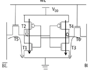
Sub-threshold leakage current is observed in SRAM cell in two locations [5] as shown in Figure 2.a)Leakage current that flows between Transistors T2 and T1 (also between T4 and T3) between the power supply rails.b)Leakage current between the bit lines (via T5 and T6) and the Ground as shown in the figure. Though there are two bit lines in the SRAM cell the leakage through them varies according to the logic value stored in the SRAM cell. When SRAM cell writes logic 1, i.e. the gate voltage and drain voltage of T6 is same (VDD) hence potentially zero current flows through it.Similarly T3 is turned off for logic 1 stored in the SRAM cell hence both the transistors are in stack thus reducing the leakage current. Hence bit line leakage is reduced. But large leakage current flows through T5 and T1.Similarly when writing logic 0 the bit line leakage is reduced through the other path i.e T5 and T1. Subthreshold leakage occurs in the transistor in the weak inversion region i.e when VGS <
Vth. Vth reduction takes place due to many factors. When
the supply voltage is to be reduced along with the technologies, the threshold voltage should be scaled proportionately. Similarly due to secondary effects of the short channel MOS transistor also the threshold voltage reduces.
The subthreshold leakage current increases exponentially with reduction in the Vth.In literature to
reduce the sub-threshold leakage the Vth of all or certain
transistors is increased. The limitation to this solution is the delay of read and write operations increase. For example if the Vth of T6 is increased either during
fabrication process(additional doping in the channel area) or by body Biasing (by changing the reverse bias voltage of the body) the wake up time or response time of the transistor increased which effects the red and write cycles. The proposed method also increases the process complexity through additional masking steps. The write delay increases when the Vth of PMOS devices is
increased while effect on read delay is negligible. The read delay increases when Vth of NMOS devices is
increased while effect on write delay is negligible. Whereas increase of Vth of T5 and T6 affects both read
[image:2.595.341.512.145.286.2]and write delay. Reducing the threshold voltage is more beneficial when write delay is less than read delay caused by additional circuitry.
Fig 2. Leakage components in SRAM cell.
B.Gate Leakage in 6T- SRAM cell
The second leakage current observed in RAM cells is gate leakage current due to tunneling effect. Due to smaller technology dimensions of sub 100nm the thickness of the oxide should be scaled down to maintain good aspect ratio. This increases the electric field across the oxide so that the charge carriers (electrons and holes tunnel towards the gate terminal). In an NMOS transistor the electrons tunnel from the body/substrate towards positively biased gate terminal. This leakage component is observed both when the device is OFF and ON conditions. Hence reducing the effect of this component saves significant amount of power. For SRAM’s used in modern computing SoC devices the number of read and write operations are more per unit time hence reducing gate leakage is very important area of research.
This tunneling current comprises of three components: a) Tunneling current due to gate overlap region in
source and drain regions. b) Gate to Channel component. c) Gate to Bulk Component.
International Journal of Emerging Technology and Advanced Engineering
Website: www.ijetae.com (ISSN 2250-2459,ISO 9001:2008 Certified Journal, Volume 3, Issue 11, November 2013)
693 To reduce the gate leakage one solution proposed is to use High-K dielectric materials or increase the thickness of the oxide. When SiO2 is used as insulating material
gate leakage is slightly is PMOS transistors [8]. Hence the leakage savings obtained through increasing the thickness is very small for PMOS transistors.In summary the subthreshold leakage component is dominant in T6, T4, T1 transistors while gate leakage is dominant in T3, T5, and T2. It doesn’t mean the component doesn’t exist in other transistors but negligible.
III.EXISTING METHOD-VARIABLE BODY BIASING METHOD
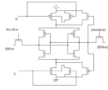
The architecture of the body biasing techniques is shown below in Fig 3 below. In this method two additional sleep transistors are added in both pull-up and pull-down network.to introduce body biasing effect the source of one PMOS device is connected to the body of the other PMOS device. Similarly the source of one NMOS device is connected to body of another NMOS device. The leakage reduction occurs both by sleep transistor effect and by body biasing effect. The PMOS transistors cannot conduct good VSS value while NMOS
transistors are not good at passing perfect VDD value. To
[image:3.595.67.249.449.601.2]restore the logic in the sleep state PMOS is used in parallel in PDN while NMOS is used in parallel in PMOS network.
Fig 3. Schematic of Variable Body Biasing
The width of the PMOS transistors is made wider than NMOS transistors for equal rise and fall times. Due to minimum aspect ratio used in sleep transistors the leakage current reduces. In the active condition Sleep=1 and Sleep bar=0. Both the sleep transistors are ON and normal read and write operations can be performed on the SRAM cell.
During the sleep mode sleep=0 and sleep bar =1 and both the sleep transistors are turned off. But due to the source of transistors tied to the body of the similar transistor the threshold voltage of the sleep transistor increases [11].As we know the increase in threshold voltage reduces the subthreshold leakage current of the transistor. Due to this the standby leakage current reduces through this approach. The purpose of additional transistors in the architecture is to retain the state in the sleep mode. To store logic one during sleep mode all the sleep transistors are off but the NMOS transistor connected parallel is the only source of power supply to the PDN.Similarly to restore logic zero the NMOS connected in parallel is the only source to Ground for PDN.the sub-threshold current is proportional to the width of the transistor, Gate voltage and threshold voltage and sub threshold swing. The circuit engineers propose leakage reduction methods by properly controlling the above parameters. In this approach the threshold voltage can be changed accordingly by changing the node voltages of the transistor. This approach is widely used in reduction of sub-threshold leakage currents in the literature. The area of the SRAM cell increases tremendously as four additional transistors are added in this approach which is a severe limitation. For an array of SRAM cells this poses a big area penalty problem. We compared the performance of variable body bias method with our proposed methods.
IV. HIGH SUPPLY VOLTAGE REDUCTION METHOD (HSVR)
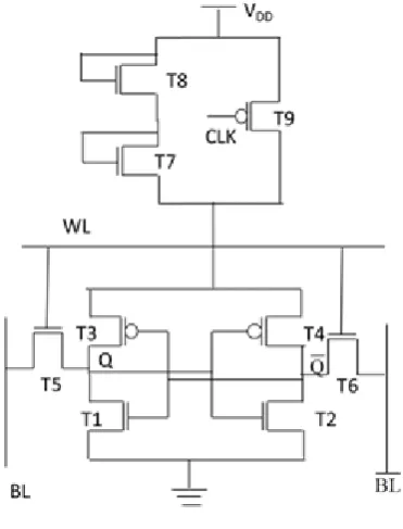
To reduce the impact of sub-threshold and gate leakage currents we added a small additional circuitry between the original power supply and the latch of the SRAM cell (Fig 4). When the SRAM cell is in active mode (during Read and Write operations) a full swing VDD is applied to
the cell. The additional transistors provide a reduced voltage drop during the standby mode across T7, T8 and T9 network.T9 is operated through clock. During the ON condition we provide alternative path between VDD and
International Journal of Emerging Technology and Advanced Engineering
[image:4.595.71.257.140.384.2]Website: www.ijetae.com (ISSN 2250-2459,ISO 9001:2008 Certified Journal, Volume 3, Issue 11, November 2013)
Fig 3. Schematic of HSVR method
Let us consider when logic 0 is stored in the cell, The gate leakage component in transistors T2,T5,T6 and T1 are considered because the component in T3 and T4 can be neglected because of PMOS nature. The gate leakage component is due to Edge Tunneling mechanism at source and drain edges (EDT). The Gate leakage is high in T1 is significant due to EDT.The subthreshold Leakage component is observed in OFF transistors of the SRAM cell i.e., T2 ,T3 and Access transistors T5 and T6.As the VDS value of the T6 is zero the subthreshold leakage component is less and can be neglected but it is maximum in the remaining Transistors (T2,T3,T5). Any Leakage reduction method should address the reduction in all these transistors.
A.Effect of HSVR on Sub-Threshold leakage reduction
In the inactive state a less voltage Vd<< VDD is applied to the source of T4 transistor hence the drain voltage of T4 and T2 reduces compared to the value when VDD is applied.
As the Access transistor T5 is OFF in inactive state, the sub-threshold leakage current remains unchanged.
Initially there is no sub-threshold leakage component in T6. But as logic value 0 is stored in the cell, an additional subthreshold leakage
B.Effect of HSVR on gate leakage reduction
As T4 is conducting and the source voltage is reduced both the gate tunneling EDT components are reduced.
When T4 is ON and the voltage at drain of T4 and T2 reduced, the gate voltage of T1 reduced. This reduces the EDT component of T1.As the VDS value of T2 Reduces
the gate leakage current reduces. The decrease in source voltage of T6 decreases one EDT component while leaving the other unchanged. (It is to be recalled that there are two EDT components of T6).Gate tunneling leakage across T5 remains unchanged as there is no voltage change on the bit bar line. As T3 is a PMOS transistor the leakage reduction is negligible. An additional gate leakage component is observed across T9 in the SRAM circuit.
V. GROUND SUPPLY VOLTAGE ELEVATION METHOD
(GSVE)
In contrast to the previous proposed method in which we reduced the higher supply voltage in this approach we raise the ground potential to reduce the sub-threshold leakage in the SRAM cell. As the ground potential is raised the voltage swing is reduced which in turn reduces the leakage current. As we know each transistor has different leakage components in standby mode the same analysis should be carried out as in the previous section. Three additional transistors are added between the ground potential and NMOS transistors of the SRAM cell. Transistor T9 acts like a control switch driven by the clock signal. Clock is enabled during the read and write operations so that full voltage swing is achieved. But during standby mode an alternative path is established between the ground and SRAM cell to raise the potential. This method is similar to diode footed cache design in which a high Vth transistor is used to raise the ground
potential.
A.Effect of GSVE on Gate leakage reduction
As we increased the Ground Potential form 0V to Vs volts, For Transistor T1 there is increase in VGS and VGD
values. This reduces the gate tunneling leakage current. For Transistor T2 the VGD potential is increased thus
International Journal of Emerging Technology and Advanced Engineering
Website: www.ijetae.com (ISSN 2250-2459,ISO 9001:2008 Certified Journal, Volume 3, Issue 11, November 2013)
[image:5.595.60.539.160.354.2]695
Table 1.
Leakage current in individual transistors of proposed methods and Variable body bias.
B.Effect of GSVE on Sub-Threshold leakage reduction
[image:5.595.332.528.523.680.2]Due to the effect of additional sub-threshold leakage component in the SRAM cell the output performance degrades when the temperature in the circuit increase. It is to be remembered that there is exponential dependency of sub-threshold leakage component with temperature. The only way left to the circuit engineers to reduce this leakage component is by changing the gate, source and drain voltages.Due to increase in source voltage of T2, the sub-threshold leakage component has reduced as it is dependent on VGS value of the MOS transistor.The subthreshold leakage components in T3 and T5 are also reduced because of variation of node voltages in the circuits due to rise in the ground potential of the circuit.
Fig 4 Schematic of GSVE method
VI. SIMULATION AND RESULTS
In the present work we compared the performance of our proposed methods against the existing Variable body Biasing.For understand the leakage reduction through our proposed methods 70nm BPTM model files are simulated in Cadence Spectre.To measure the runtime leakage current we simulated the SRAM cell for 10 Read and Write cycles. During the standby mode the clock is not applied to the control switch of the cell thus reducing the VDD value in HSVR method and increasing the ground potential in GSVE method. The schematic of the conventional SRAM cell and HSVR and GSVE methods are shown in figures 5, 6, and 7
Fig 5. Schematic of conventional SRAM cell.
Transistor Leakage
component (nA)
Conventional SRAM (nA)
HSVR-SRAM(nA) GSVE-SRAM(nA)
T1
IG 37.1 2.38 2.35
Isub 29.3 28.9 29.1
T2
IG 13.9 1.14 1.08
Isub 16.8 2.38 1.79
T3
IG 12.47 11.43 10.83
Isub 0.86 0.58 0.17
T4
IG 23.31 2.49 3.46
Isub 0.56 0.56 0.29
T5
IG 9.84 9.84 8.34
Isub 0.62 0.62 0.31
T6
IG 19.5 18.43 19.21
[image:5.595.99.225.540.698.2]International Journal of Emerging Technology and Advanced Engineering
[image:6.595.292.542.158.480.2]Website: www.ijetae.com (ISSN 2250-2459,ISO 9001:2008 Certified Journal, Volume 3, Issue 11, November 2013)
Table 2.
Leakage power comparison between Variable body Bias and HVSR, GSVE.
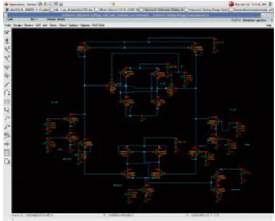
Fig 6. Schematic of HSVR method.
[image:6.595.47.540.165.493.2]The subthreshold leakage components and gate tunneling leakage components in each of the transistors with comparison between our proposed methods and conventional SRAM is given in Table 1.The following conclusions can be drawn from the measured leakage current of different transistors comparing conventional SRAM and HSVR-SRAM. In T1 transistor the gate and subthreshold leakage components reduced to 6.5 % of the value in the conventional SRAM cell while subthreshold leakage component remains unchanged. In T2 transistor the gate leakage component is reduced to 8.2 % of the initial value while subthreshold leakage component reduced by 86 %.In T3 not much gate leakage current and subthreshold leakage current savings are observed. As it is a PMOS device the gate leakage can be neglected. In T4 transistor the gate leakage component reduced by 89% while subthreshold leakage reduction is not observed. In T5 transistor there is no reduction in gate
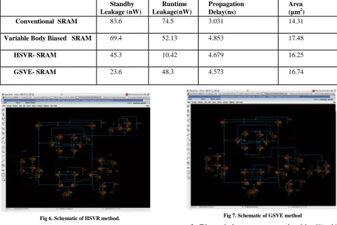
Fig 7. Schematic of GSVE method
In T6 gate leakage component reduced by 4% while subthreshold leakage component increased by 40%. The following conclusions can be drawn from the measured leakage current of different transistors comparing conventional SRAM and GSVE-SRAM.In T1 the gate leakage component reduced to 7 % of its initial value in conventional SRAM cell but there is no change in the sub-threshold leakage component. In T2 gate leakage component reduced to 7.7 % of its value in conventional SRAM cell while subthreshold leakage component reduced by 89 % which is a significant value. In T3 subthreshold leakage current reduced by 80 % while gate leakage current reduced only by only 14%.In T4 the gate leakage current is reduced by 85 % while subthreshold leakage component reduced by 50 %.In T5 the gate leakage reduced by 15 % while subthreshold leakage current reduced by 50%.In T6 there is no reduction in gate leakage while subthreshold leakage reduced by 5% which
Standby
Leakage (nW)
Runtime Leakage(nW)
Propagation Delay(ns)
Area (µm2)
Conventional SRAM 83.6 74.5 3.031 14.31
Variable Body Biased SRAM 69.4 52.13 4.853 17.48
HSVR- SRAM 45.3 10.42 4.679 16.25
International Journal of Emerging Technology and Advanced Engineering
Website: www.ijetae.com (ISSN 2250-2459,ISO 9001:2008 Certified Journal, Volume 3, Issue 11, November 2013)
697 In addition to the above reduction in the leakage components an additional EDT gate leakage current is observed in T9 for HSVR method. Though we measured the leakage reduction for each individual transistor, the Resultant leakage value is calculated by the simulator and is given in Table 2. It is observed that HSVR method is best suited for reduction of gate leakage current while GSVE is suitable for reduction of sub-threshold leakage reduction. The standby leakage and active leakage, Area are compared with Variable Body Biasing methods versus the proposed methods are shown in table 2. From the above measured values the propagation delay of HSVR and GSVE is slightly higher than Conventional SRAM, less than variable body bias method which has four additional transistors added to the SRAM cell. Due to additional transistors there is slight increase in area for the proposed SRAM cells. In HSVR the runtime leakage current reduced by 86 % compared to conventional SRAM cell as gate leakage current reduced in most off
the transistors when the cell is in the operating mode. In GSVE method the standby leakage current reduced by 72 %.
VII. CONCLUSION
The present work analyzes the latest developments in low-power circuit techniques and methods with an emphasis on SRAMs. Many of reviewed techniques are applicable to other applications such as ASICs, DSPs, etc. Battery and solar-cell operation requires an operating voltage environment in low voltage area. These conditions demand new design approaches and more sophisticated concepts to retain high device reliability.
The proposed techniques (HSVR and GSVE) are topology based and hence easier to implement. The substantial reduction in leakage currents obtained proves them to be as effective as any fabrication level technique would be.
REFERENCES
[1] K. Hardee et al., "A 0.6V 205MHz 19.5ns IRC 16Mb Embedded
DRAM," 2004 ISSCC Dig. Tech. Papers, pp. 494-495, Feb2004.
[2] K. Itoh, VLSI Memory Chip Design, Springer-Verlag, NY,2001.
[3] Y. Nakagome et al., "Review and prospects of low-voltage RAM
circuits," IBM J. R & D, vol. 47, no. 5/6, pp. 525-552, Sep. /Nov. 2003.
[4] K. Itoh et al., "Reviews and Prospects of Low-voltage Embedded
RAMs," CICC2004 Dig. Tech. Papers, pp. 339-344, Oct. 2004.
[5] KIM, C. and ROY, K., “Dynamic Vt SRAM: a Leakage Tolerant
Cache Memory for Low Voltage Microprocessors,” Proceedings of the International Symposium on Low Power Electronics and Design, pp. 251–254, August 2002.
[6] A. Agarwal, C. Kim, S. Mukhopadhyay, and K. Roy, “Leakage in
nano-scale technologies: mechanisms, impact and design considerations,“ in Proc. of Design Automation Conf.,2004 [7] K. Itoh and K. Sasaki, Trends in low power circuit design, Proc.
IEEE, Vol. 83, pp 524-543, 1993.
[8] K. Itoh “Trends in Low-Power RAM Circuit Technologies",
Proceedings of the IEEE, April 1995.
[9] G. Razavipour, A. Afzali-Kusha “Design and Analysis of Two
Low-Power SRAM Cell Structures” IEEE Transaction on very large scale integration systems, VOL. 17, NO. 10, Oct. 2009.
[10] Tajrian Izma,Parag Barua,Md.RekaurRahamn,Priyanka Sen Gupta
.” Novel approaches to Low leakage and Area Efficient VLSI design, ICEVIS 2012, May pp 316-324.
[11] http://www.edaboard.com/thread108793.html
[12] Zhang Zheng-xuan, Zhang En-xia “Practical considerations in the