Pulsed Latch Based Area - Low - Delay Effective
Shift Register
Sai Kumar1, Radhika Reddy2
1
P G student, M. Tech, 2Associate Professor JITS, Karimnagar
Abstract: With so many events happening in the world at a very fast pace the human race is in search for new technological advancements. There is a high demand for minutely packed power devices that have higher efficiency of area which has lead the industry of VLSI to venture into the unknown. As technology moves into these levels the power management requirement of the devices rise. This paper proposes allow power and area-efficient shift register using pulsed latches. The area and power consumption are made to reduce by substituting flip-flops with pulsed latches. The timing difficulty in the pulsed latches that originate out of the use of conventional single pulsed clock signal is taken care of by the use of multiple nonoverlap delayed pulsed clock signals. The shift register uses a small number of the pulsed clock signals by grouping the latches to several sub shifter registers and using additional temporary storage latches.
I. INTRODUCTION
Technology has invaded into the life of human beings to such deep extent that today everyone has a wish for smaller faster fancier gadgets. This wish has been granted to them by the technological developments in the field of VLSI technology. A SHIFT register is the basic building block in a VLSI circuit. Shift registers find them to be use full commonly in many applications, such as digital filters, communication receivers, and image processing ICs. Now a days, as there is high demand of images with utmost clarity the size of the image data continues to increase, the word length of the shifter register increases to process large image data in image processing ICs. An image-extraction and vector generation VLSI chip uses a 4K-bit shift register. A 10-bit 208 channel output LCD column driver IC uses a 2K-bit shift register. A 16-megapixel CMOS image sensor uses a 45K-bit shift register. As the word length of the shifter register increases, the area and power consumption of the shift register become important design considerations.
II. BASIC CONCEPT
The designing of a shift register is quite simple. An n bit shift register is composed of series connected N data flip-flops.The speed of the flip flops is of no major constraint here as there are no connections between the shift registers and flip flops. The smallest flip flop is enough to drive the requirement of the shift register and for this same reason the pulsed latches have replaced the flip flops as they are much smaller in size Vis a Vis the flip flops there by reducing power consumption. Although there are some drawbacks like that of the timing problem, which is easy to overcome by the use of multiple clocked pulses instead of a simple single pulsed clock. The shift register uses a small number of the pulsed clock signals by grouping the latches to several sub shifter registers and using additional temporary storage latches.
A. Review flip-flops and latches
In electronics, a flip-flop or latch is a circuit that has two stable states and can be used to store state information. A flip-flop is a bi stable multi vibrator. The circuit can be made to change state by signals applied to one or more control inputs and will have one or two outputs. It is the basic storage element in sequential logic. Flip-flops and latches are fundamental building blocks of digital electronics systems used in computers, communications, and many other types of systems. Flip-flops and latches are used as data storage elements. A flip-flop stores a single bit (binary digit) of data; one of its two states represents a "one" and the other represents a "zero". Such data storage can be used for storage of state, and such a circuit is described as sequential logic. When used in a finite-state machine, the output and next finite-state depend not only on its current input, but also on its current finite-state (and hence, previous inputs). It can also be used for counting of pulses, and for synchronizing variably-timed input signals to some reference timing signal.
III. PROPOSED SHIFT REGISTER
power consumption. The Pulsed latch schematic is shown in fig. 1For the pulsed clock signal all the pulsed latches share the pulse generation circuit. Due to this sharing of the pulse generation circuit the area and power consumption of the circuits reduces to almost half of the master slave flip flop. It has a drawback that the pulsed clock generator can’t be used directly on this circuit due to its timing problems. To overcome this various steps can be implemented such as – • to add delay circuits between latches • use multiple non-overlap delayed pulsed clock signals All though both the above mentioned methods solve the timing problem the delay circuits present challenge in the area and power consumption domain ,so it is best in the interest of low power and area designing to make use of the non over lapping multiple delayed pulse clock signals.
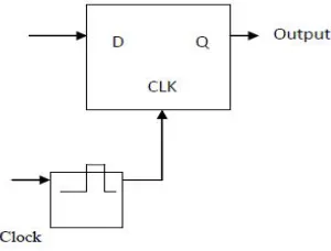
Fig.1. Pulsed Latch
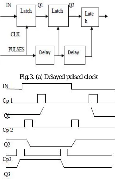
The Shift Register consists of several latches as shown in fig.
2. (a) The output signal of the first Latch (Q1) changes because the input signal (IN) is constant during the clock pulse width (TPULSE). The second Latch has an output signal (Q2) which depends on the output of (Q1). The output waveform is shown in fig. 2. (b).
Fig. 2 (a) Shift Register with Latches.
Fig. 2 (b) Waveform of Shift Register
[image:3.612.211.385.399.683.2] [image:3.612.214.390.403.529.2]Fig.3. (a) Delayed pulsed clock
Fig.3 (b) waveform of Delay circuit
B. Clock Pulse Circuit
Each pulsed clock signal arrives at the sub Shift Registers at different time due to the pulse skew in the wire. The pulse skew increases proportional to the wire distance from the delayed pulsed clock generator. All pulsed clock signals have almost the same pulse skews when they arrive at the sub Shift
Register. Therefore in the sub Shift Register, the pulse skew differences between the pulsed clock signals are very small. The clock pulse intervals larger than the pulse skew
Differences cancel out the effects of the pulse skew Differences.
Another solution is to insert the clock buffers and
[image:4.612.212.397.92.378.2]clock trees to send the short clock pulse with a small wire delay. But, this increases the area and power overhead. Moreover, the multiple clock pulses make the more overhead for multiple clock buffers and clock trees. The schematic of clock pulse circuit is shown in Fig.4
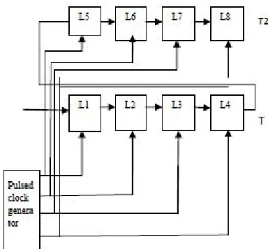
[image:4.612.207.397.571.702.2]A Shift Register is a sequential circuit in which the binary bits shift either towards left or right on each clock transition. The pulse skew increases proportional to the wire distance from the delayed pulsed clock generator. All pulsed clock signals have the same pulse skews when they arrive at the sub Shift Registers. Therefore, in the sub Shift Registers, the pulse skew differences are very small. The clock pulse intervals, larger than the pulse skew differences cancel out the effects of the pulse skew differences. Also, the pulse skew differences between the different sub Shift Registers do not cause any timing problem. The proposed Shift Register and its waveform are shown in fig. 5(a) and fig. 5(b). The Latches are denoted as L1, L2, L3, L4, L5, L6, L7 and L8. CP1, CP2, CP3, CP4 are the clock pulses.
Fig. 5 Shift Register with pulsed clock generator
D. SSASPL-Latch
T 1 A latch can capture data only when the clock is enabled. If the pulse clock triggers a latch, then latch is synchronized similar to the edge triggered flip flop. The pulsed generators generate the pulsed clock waveforms with a source clock. SSASPL– latch is Static differential Sense Amplifier Shared Pulse Latch. This latch is the smallest latch. This latch has 9 transistors. In the proposed Shift Register this latch has been modified with transistors by removing an inverter in the circuit. The schematic of the SSASPL-latch can be referred. This SSASPL-latch updates the data and holds the data.
IV. SIMULATION RESULTS
[image:5.612.177.437.516.704.2]Fig: Pulsed Clock schematic
Fig: SSASPL schematic
[1] Byung - Do Yang, “Low-power and Area-efficient Shift Register using Pulsed latches,” IEEE Transactions on circuits and systems-I: Regular papers, Vol. 62, NO. 6, JUNE 2015.
[2] P. Reves, P. Reviriego, J.A. Maestro, and O. Ruano, “New protection techniques against SEUs for moving average filters in a radiation environment,” IEEE Trans. Nucl. Sci.,vol. 54, no. 4, pp. 957 - 964, Aug.2007.
[3] M. Hatamian et al., “Design considerations for gigabitEthernet 1000 base-T twisted pair transceivers,” Proc. IEEE Custom Int. Circuits Conf., pp. 335 - 342, 1998.
[4] H. Yamasaki and T. Shibata,” A Real-time image feature extraction and vector-generation VLSI employing arrayed shift register architecture,” IEEE J. Solid-State Circuits, vol. 42, no. 9, pp.2046-2053, sep. 2007.
[5] H-S. Kim, J .- H. Yang, S. –H. Park, S. – T. Ryu, and G. – H. Cho, “A 10 bit column driver IC with parasitic insensitive iterative charge sharing based capacitor string interpolation for mobile active matrix LCDs.
[6] S. Heo, R. Krashinsky, and K. Asanovic, “Activity sensitive flip flop and latch selection for reduced energy, ” IEEE Trans. Very Large Scale Integer. (VLSI) Syst., vol. 15, no. 9, pp. 1060-1064. Sep. 2007.
[7] S. Naffziger and G. Hammond, “ The implementation of the next generation 64 bit Itanium microprocessor,” in IEEE Int. Solid state circuits Conf. (ISSCC) Dig. Tech. Papers, pp. 138 – 139, Feb. 2002, pp. 276 – 504.
[8] H. Partovi et al.,” Flow through latch and edge triggered flip flop hybrid elements,” IEEE Int. Solid state Circuits Conf. (ISSCC) Dig. Tech. Papers, pp. 138 – 139, Feb. 1996.
[9] E. Consoli, M. Alioto, G. Palumbo, and J. Rabaey, “Conditional push pull pulsed latch with 726 flops Energy delay product in 65nm CMOS,” in IEEE Int. Solid State Circuits Conf. (ISSCC) Dig. Tech. Papers, Feb. 2012, pp. 482 – 483.