Technology (IJRASET)
Comparative Study of Various Binary Floating
Point Multiplier Techniques Using VHDL
Rupali Umekar#1, Dr.Vasif Ahmed*2
Department Of EXTC, B.N.C.O.E Pusad, India
Abstract-In computing, floating point describes a method of representing an approximation of a real number in a way that can support a wide range of values. Low power consumption and smaller area are some of the most important criteria for the fabrication of DSP systems and high performance systems. Optimizing the speed and area of the multiplier is a major design issue. However, area and speed are usually conflicting constraints so that improving speed results mostly in larger area in implementation of the system. This project presents study of various binary floating point multiplier techniques using various Algorithms of an IEEE 754 single precision floating point multiplier targeted for Altera. Now a days there is a scope of advance technology in which the design of more efficient multiplier is dominant part of digital system. This objective of this study is to find algorithm which offers higher speed and low power consumption. Subsequently, tradeoffs between area and delay parameters for each multiplier design are also analyzed for the different schemes. This approach is well-suited for several complex and portable VLSI circuits. In this work, the comparative study of Booth multiplier, Dadda multiplier, Wallace Tree multiplier are carried out by analyzing area, power and delay characteristics with particular importance on low power consumption.
KEYWORDS:- WALLACE ALGORITHM,BOOTH ALGORITHM,DADDA ALGORITHM,FLOATING POINT MULTIPLIER.
I. INTRODUCTION
Floating point numbers are one possible way of representing real numbers in binary format; the IEEE 754 standard presents two different floating point formats, Binary interchange format and Decimal interchange format. Multiplying floating point numbers is a critical requirement for DSP applications involving large dynamic range. FPGAs are increasingly being used in the high performance and scientific computing community to implement floating-point based hardware accelerators. FPGAs are generally slower than their application specific integrated circuit (ASIC) counterparts, as they can't handle as complex a design, and draw more power. However, they have several advantages such as a shorter time to market, ability to re-program in the field to fix bugs, and lower nonrecurring engineering cost. Vendors can sell cheaper, less flexible versions of their FPGAs which cannot be modified after the design is committed. The development of these designs is made on regular FPGAs and then migrated into a fixed version that more resembles an ASIC.
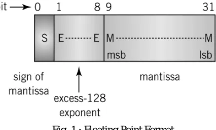
[image:2.612.195.408.568.696.2]The floating point is a method of representing anapproximation of a real number in a such way that can support a tradeoffbetween range and precision. A number is, in general, represented approximately to a fixed number of significand digits. The term floating point numbers is derived from the fact that there is no fixed number of digits before and after the decimal point, that is, the decimal point can float.
Fig. 1 : Floating Point Format
Technology (IJRASET)
of the significand then the number is said to be a normalized number.
II. PROPOSED WORK
Most of the DSP applications need floating point numbers multiplication. In binary format, floating point numbers are represents two floating point formats, Binary interchange format and Decimal interchange format. The binary formats are called ‘Single precision’ and ‘Double precision respectively.
The single-precision (32-bit) floating-point multiplier performs multiplication of two inputs which are floating-point numbers. At the beginning, both inputs must be converted from decimal number into floating point representation based from IEEE 754 standard before doing the multiplication. Once the floating point multiplication is complete, the output which is in IEEE 754 floating point representation will convert back to decimal number.
A multiplication of two floating-point numbers is done in the following 5 steps: Step 1: Multiplication of mantissas
Step 2: Normalization
Step 3: Addition of the exponents
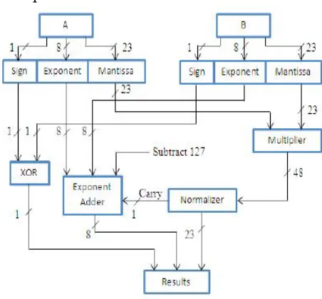
[image:3.612.189.415.271.481.2]Step 4: Calculation of the signStep 5: Composition of all results
Fig. 2. 32-bit floating point multiplier data flow
Fig. 2 describes the 32-bit floating point multiplier data process flow. Each input is split into three modules (sign, exponent, and mantissa) so that can be easily to route into corresponding components. Signs from input A and B are connected directly to XOR gate to generate the final sign result, ‘0’indicates positive sign and ‘1’ indicates the negative sign. Meanwhile, exponents and mantissas from input A and B are connected to exponent adder and multiplier respectively. The 48- bit output from multiplier must pass through to the normalizer to perform rounding to nearest 23-bit of mantissa. In exponent adder, both exponents from A and B are added before subtract to bias value which is 127. The carry signal from normalizer is also connected to exponent adder to adjust the exponent value, which will be the final 8-bit exponent result. All the output from signer (1-bit), exponent adder (8-bit), and normalize (23-bit) are then combined to form 32-bit floating point multiplication product as the final results. The last 23 bits of mantissa in 32-bit floating point number is given by two operands for multiplication. The explicit ‘1’ added as the leading bit of both mantissas to fit into 24-bit multiplier unit.
III. COMPARATIVE STUDY OF VARIOUS MULTIPLIER TECHNIQUES
A comparatively study of various multiplier techniques depending on the area, power consumption and speed of multiplication is carried out which is discussed below:
A. Wallace Multiplier
Technology (IJRASET)
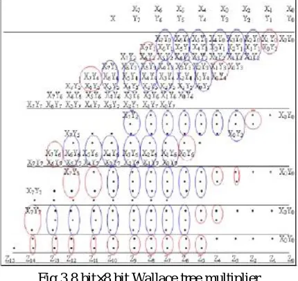
[image:4.612.199.414.94.297.2]the addition of partial products.
Fig 3 8 bit×8 bit Wallace tree multiplier
Step 1: Generation of Partial products
The first step is similar to normal binary multiplication that we use. This step generates Partial products (PPs). The elements a0b1 to a3b3 are called partial products (pp). Each PP has its place weight in powers of 2. Weight of a partial product aibj is given by 2x where x=i+j.
Step 2: Reduction Stages:
Now the generated partial products are added using ‘Half adders’ and ‘Full adders’. Following guide lines are followed in the addition process.
1) If the column has only one partial product it can be directly propagated to the output in the same column (sum output of same
weight). No reduction is necessary.
2) If the column has two partial products only, a half adder is to be used to generate sum output of same weight and carry output of next weight.
3) If the column has 3 or more PPs, we have to use at least one full adder. As many full adders are used as possible because, a full adder will reduce 3 PPs at a time into sum and carry.
4) Addition of any two PPs results in two outputs:
i) The sum bit
ii) The carry bit
5) Sum bit is of weight 2x and carry bit is of weight 2x+1 where ‘x’ is the weight of partial products of that addition operation.
6) After addition, the sum bit remains in same column for next stage reduction and carry bit propagates to next left column for next stage reduction.
7) When only two rows of PPs are left over, for the final reduction stage, we use a parallel adder to give the final output
B. Dadda Multiplier
Dadda proposed a sequence of matrix heights that are predetermined to give the minimum number of reduction stages. To reduce the N by N partial product matrix, dada multiplier develops a sequence of matrix heights that are found by working back from the final two-row matrix. In order to realize the minimum number of reduction stages, the height of each intermediate matrix is limited to the least integer that is no more than 1.5 times the height of its successor. The process of reduction for a dadda multiplier is developed using the following recursive algorithm
1) Let d1=2 and dj+1 = [1.5*dj], where dj is the matrix height for the jth stage from the end. Find the smallest j such that at least one column of the original partial product matrix has more than dj bits.
2) In the jth stage from the end, employ (3, 2) and (2, 2) counter to obtain a reduced matrix with no more than dj bits in any column.
Technology (IJRASET)
[image:5.612.190.422.153.379.2]utilizes the minimum number of (3, 2) counters. {Therefore, the number of intermediate stages is set in terms of lower bounds: 2, 3, 4, 6, 9 . . .For Dadda multipliers there are N2 bits in the original partial product matrix and 4.N-3 bits in the final two row matrix. Since each (3, 2) counter takes three inputs and produces two outputs, the number of bits in the matrix is reduced by one with each applied (3, 2) counter therefore}, the total number of (3,2) counters is #(3, 2) = N2 – 4.N+3 the length of the carry propagation adder is CPA length = 2.N–2.
Fig. 4 Dot diagram for 8 by 8 Dadda Multiplier
The number of (2, 2) counters used in Dadda’s reduction method equals N-1.The calculation diagram for an 8X8 Dadda multiplier shown in fig. 4. Dot diagrams are useful tool for predicting the placement of (3, 2) and (2, 2) counter in parallel multipliers. Each IR bit is represented by a dot. The output of each (3, 2) and (2, 2) counter are represented as two dots connected by a plain diagonal line. The outputs of each (2, 2) counter are represented as two dots connected by a crossed diagonal line. The 8 by 8 multiplier takes 4 reduction stages, with matrix height 6, 4, 3 and 2. The reduction uses 35 (3, 2) counters, 7 (2, 2) counters, reduction uses 35 (3, 2) counters, 7 (2, 2) counters, and a 14-bit carry propagate adder. The total delay for the generation of the final product is the sum of one AND gate delay, one (3, 2) counter delay for each of the four reduction stages, and the delay through the final 14-bit carry propagate adder arrive later, which effectively reduces the worst case delay of carry propagate adder. The decimal point is between bits 45 and 46 in the significand IR. The critical path starts at the AND gate of the first partial products passes through the full adder of the each stage, then passes through all the vector merging adders.
C. Booth Multiplication Algorithm for Radix-4
The Booth multiplication algorithm was developed by a British electrical engineer, physicist and computer scientist Andrew Booth in 1950 [6]. One of the solutions of realizing high speed multipliers is helps to decrease the number of subsequent calculation stages. The original version of the Booth algorithm (Radix-2) had two drawbacks. They are
1) The number of add subtract operations and the number of shift operations become variable and become inconvenient in designing parallel multipliers.
2) The algorithm becomes inefficient when there are isolated 1’s. These problems are overcome by using modified Radix-4 Booth
multiplication algorithm.
This algorithm scans strings of three bits as follows:
1) Extend the sign bit 1 position if necessary to ensure that n is even.
2) Append a 0 to the right of the LSB of the multiplier.
Technology (IJRASET)
The state diagram of the Radix-4 Booth multiplier is shown below. It consists of eight different types of states and during these states we can obtain the outcomes, which are multiplication of multiplicand with 0,-1 and -2 consecutively. The pictorial view of the state diagram presents various logics to perform the Radix-4 Booth multiplication in different states as per the adopting encoding technique.
The state diagram of the Radix-4 Booth multiplier is shown below. It consists of eight different types of states and during these states we can obtain the outcomes, which are multiplication of multiplicand with 0,-1 and -2 consecutively. The pictorial view of the state diagram presents various logics to perform the Radix-4 Booth multiplication in different states as per the adopting encoding technique.
[image:6.612.204.407.89.183.2]
Fig. 5 Booth Radix-4 FSM State Diagram
The design has five input ports ("clk", “n_reset”, “start”, “mcand”, and "mplier”) and two output ports (“done” and “product”). The multiplier requires a start pulse to initialize the FSM with values from the “mcand” and “mplier” inputs and put the FSM in the “BUSY” state. Math steps can be sequenced by using the “start” and “done” signals between instantiations.
IV. SIMULATION RESULT
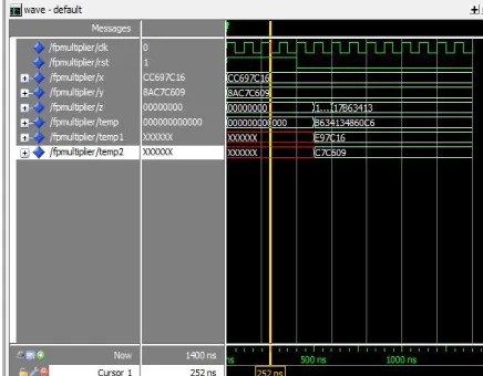
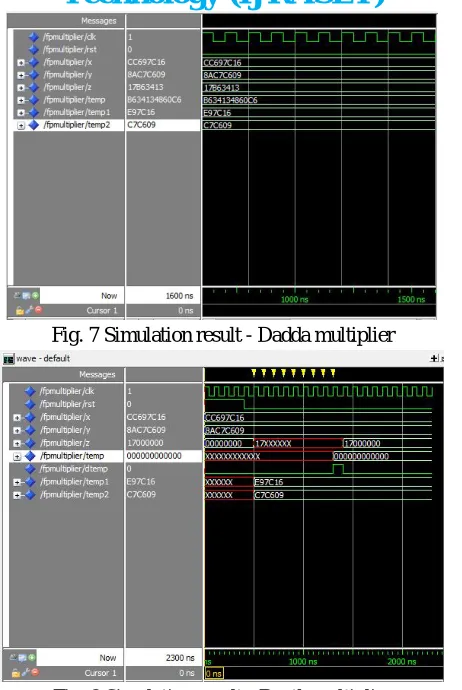
The simulation results for corresponding inputs are shown in Fig. The design has been simulated by using ModelSim. Consider inputs to the floating point multiplier are:
A = CC697C16 B = 8AC7C609
The output of the multiplier is 17B63413
Fig. 6, 7 and 8 show the snapshots taken from ModelSim after the timing simulation of the floating point multiplier for Wallace multiplier, Dadda multiplier and Booth multiplier
[image:6.612.196.414.540.710.2]Technology (IJRASET)
[image:7.612.195.426.71.416.2]Fig. 7 Simulation result - Dadda multiplier
[image:7.612.169.435.441.692.2]Fig. 8 Simulation result - Booth multiplier
Table 2- Comparison table for various floating point Multipliers
Algorithm Area Power(mW) Delay(ns)
Wallace 1172 78.05 8.40
Dadda 1233 78.09 9.18
Booth 430 78.08 9.6
0 200 400 600 800 1000 1200 1400
Wallace Dadda Booth
Area 3-D Column 2 3-D Column 3
Technology (IJRASET)
V. CONCLUSION
Here we have studied different multipliers and concluded that booth multiplication gives good performance in terms of area. Wallace multiplication is one of the suitable algorithm to be used to design the high speed multiplier because it has less gate delay and able to perform such complex multiplication faster .
REFERENCES
[1] “A High Speed Wallace Tree Multiplier Using Modified Booth Algorithm for Fast Arithmetic Circuits” Jagadeshwar Rao M1, Sanjay Dubey2ISSN: 2278-2834, ISBN No: 2278-8735 Volume 3, Issue 1 (Sep-Oct 2012), PP 07-11
[2] Addanki Puma Rameshl, A. V. N. Tilak2, A.M.Prasad3 “An FPGA Based High Speed IEEE754 Double Precision Floating Point Multiplier Using Verilog.” 978-1-4673-5301-4/13/$31.00 ©2013 IEEE
[3] “Efficient Hybrid Method for Binary Floating Point Multiplication” S. Praveenkumar Reddy et al Int. Journal of Engineering Research and Applications www.ijera.com ISSN : 2248-9622, Vol. 4, Issue 4 ( Version 3), April 2014, pp.37-42
[4] “A High Speed Binary Floating Point Multiplier Using Dadda Algorithm” Dr C.V.krishna Reddy, Dr K. Sivani, 978-1-4673-5090-7/13/$31.00 ©2013 IEEE [5] “Comparative Study and Analysis of Fast Multipliers”. Deepika Purohit, Himanshu Joshi International Journal of Engineering and Technical Research (IJETR) ISSN: 2321-0869, Volume-2, Issue-7, July 2014
[6] A. Booth, A Signed Binary MultiplicationbTechnique, Journal of Mechanics and Applied Mathematics, Vol. 4, 1951, pp. 236-240.