N A N O E X P R E S S
Open Access
On the Current Drive Capability of Low
Dimensional Semiconductors: 1D versus 2D
Y. Zhu
*and J. Appenzeller
Abstract
Low-dimensional electronic systems are at the heart of many scaling approaches currently pursuit for electronic applications. Here, we present a comparative study between an array of one-dimensional (1D) channels and its two-dimensional (2D) counterpart in terms of current drive capability. Our findings from analytical expressions derived in this article reveal that under certain conditions an array of 1D channels can outperform a 2D field-effect transistor because of the added degree of freedom to adjust the threshold voltage in an array of 1D devices.
Keywords:Low-dimension semiconductor, Electron transport, Current drive capability
Background
The trend of scaling CMOS technology toward ever smaller dimensions has resulted in device structures that resemble nanowires in terms of their cross-sectional dimensions, i.e., FinFETs and TriGates [1–6] are approaching heights and widths of few tens of nanometers. Depending on the nature of the channel material, and in particular if materials other than sili-con are sili-considered, size quantization effects can be relevant [7, 8] in these types of structures. Envisioning that the current trend of miniaturization prevails, one-dimensional modes will ultimately carry the current from source to drain. In other words, in order to con-tinue channel length scaling, low-dimensional channel structures are introduced at the expense of lower current drive capabilities per wire. To compensate for the loss of material that is introduced by separating the individual wire structures, arrays of the same have to be built. The obvious question arising in this con-text is“Under which circumstances does this approach make sense and when does it fail or–as we will show below–under which conditions is it desirable to oper-ate in the one-dimensional transport mode regime even without requiring the additional benefit of chan-nel length scaling”[9–13].
To shine some light on these questions, we have stud-ied a model system that consists of a two-dimensional
gated channel with ideal source/drain contacts operating in the ballistic regime. This system is then “patterned” into individual one-dimensional channels of various dimensions and spacing between them. Note that the structures under consideration remain planar and do not provide the added advantage of effectively increasing the device width in the vertical direction (as in the case of FinFETs and TriGates). A comparison between both the on- and off-state performance of the various systems when operating in the quantum capacitance limit, i.e., the conduction and valence bands of the structure are under ideal gate control, reveals the desired operation window for low-dimensional nanowire arrays which goes beyond the arguments that typically motivate the intro-duction of FinFETs and TriGates.
Methods
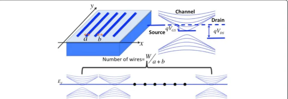
Let us consider an array of 1D nanowires with widtha that is separated by a gap of dimensionb, as shown in Fig. 1. The total width of the array is assumed to be W=n⋅(a+b), where n is the number of wires.
Manipulating aandb and comparing the conductivity
of the array with a 2D film of width W allow gaining insights into the impact of size quantization and, as will be shown, indicate a window of operation for which an array of 1D wires can outperform a 2D film despite the material loss associated with introducing “cuts”of widthb.
To perform a quantitative analysis, we first consider gra-phene and then extend our calculation to a semiconductor * Correspondence:[email protected]
Birck Nanotechnology Center, Purdue University, West Lafayette, IN 47907, USA
© 2015 Zhu and Appenzeller.Open AccessThis article is distributed under the terms of the Creative Commons Attribution 4.0 International License (http://creativecommons.org/licenses/by/4.0/), which permits unrestricted use, distribution, and reproduction in any medium, provided you give appropriate credit to the original author(s) and the source, provide a link to the Creative Commons license, and indicate if changes were made.
Zhu and AppenzellerNanoscale Research Letters (2015) 10:425
with parabolic E(k) relation. Starting from the two-dimensional linear energy dispersion of graphene around the Dirac point, size quantization results in a set of one-dimensional modes as depicted in Fig. 1. The actual energy spacing between the individual 1D
modes becomes larger (including the band gap) if a
becomes smaller. At the same time, the number of
modes M1D(E) becomes discrete in 1D. The band
lineup under zero gate and drain bias conditions for each 1D wire is defined as the minimum of the lowest conduction band edgeEC0in the channel aligning with the source and drain Fermi levels in the contacts. All wires are assumed to respond in the same manner to the gate and drain field (see bottom part of Fig. 1). In case of the 2D graphene film, the threshold voltage is defined as the Dirac point. Through this approach of setting the threshold voltage to zero for both 1D wires and 2D films at the conduction band edge, a compari-son of the device on-state needs to be concerned only
with the gate voltage VGS rather than the overdrive
voltageVGS−Vth.
Under the conditions discussed above, the current through the device can be calculated using Landauer formalism. For ease of handling the analytical expres-sions, zero temperature conditions and ballistic trans-port in the quantum capacitance limit (QCL) are assumed. In the appendix, our calculations are ex-tended toward 300 K (Additional file 1: Figure S1) showing that the analytical results obtained forT= 0 K as discussed in the following capture all relevant aspects and allow to understand the critical trends even quantitatively.
Within this model the electron current density (which is the only component considered) can be writ-ten as
I2D¼W
q h
Z
EC
M2DðfS−fDÞdE ð1Þ
Here, q is the electron charge, M2D is the number of propagating modes per unit width in the 2D device,
M2D¼h2D2DÄnveff, D2D is the full density of states (in-cluding +k and −k-states),veff is the average electron velocity in transport direction, and fS and fD are the source and drain Fermi distributions, respectively.
If a positive gate bias is applied, the bottom of the conduction band is pulled down by exactly the amount
of qVGS because of the assumed operation in the
quantum capacitance limit (QCL) [14, 15] and a positive drain voltage moves the drain Fermi level down byqVDS. Note that the assumption of operation in the QCL is justified for materials with low density of states when aggressively scaled gate oxides are considered. Further-more, it should be noted that operation in the QCL is harder to achieve in the 2D case than for 1D due to the larger density of states in 2D. Thus, assuming that both 1D and 2D follow a one-to-one band movement with the gate voltage will potentially underestimate (but not overestimate) the amount of current by which the 1D current can surpass its 2D counterpart.
To calculate the current through the graphene transis-tor we note that (i) the current in a uniform 2D system is proportional to the device width W, (ii) the energy dispersion E(k) of graphene close to the Dirac point can be approximated by E=vfℏk, and (iii) the density of states (DOS) isD2D¼g⋅2πE=h2v2f, wheregis the
degen-eracy factor, which is 4 for graphene—accounting for spin and valley degeneracy. To simplify the following calculations, we setgto 1. Furthermore, (iv) the average
Fig. 1Model system (top left), impact of VDSand VGSon the 1D mode system (top right), and visualization of parallel conduction in an array of 1D
[image:2.595.60.539.90.255.2]velocity in two dimensions isveff= 2vf/π. Under these as-sumptions, we find
I2D¼
W q3
h2vf
V2GS VGS<VDS
I2D¼
W q3
h2vf
2VDSVGS−V2DS
VGS>VDS
8 > > > > < > > > > :
ð2Þ
On the other hand, the current in a one-dimensional system is carried by 1D modes with discrete k-vector values in the quantization direction. For simplicity, we assume here hard wall potentials at the edges of the wires with width a, resulting in an energetic spacing between modes ofΔE=hvf/2a. This is a simple yet valid assumption if comparing our findings with results from first-principle calculation [16, 17]. Only modes in the energy interval between the source and the drain Fermi level contribute to the current. Moreover,D1D⋅v1D= 2/h for g= 1, independent of the actual energy dispersion. Assuming again zero temperature conditions and ballis-tic transport in the quantum capacitance limit as in the 2D case and noting that veff=vf in the 1D case, the 1D current can be expressed as
I1D¼n
q h
Z
M1Dð ÞE ðfS−fDÞdE ð3Þ
Here, n=W/(a+b) is the number of wires,m(E) is the number of modes at each energy,M1D(E) = int[(E+qVGS)/
ΔE] + 1 forE>−qVGS, andm(E) = 0 forE<−qVGS. Only currents due to electron flow in the conduction band are considered. It seems apparent that the current through an array of 1D structures cannot exceed the 2D current for finiteb-values. Interestingly, this statement isonlycorrect for qVGS and qVDS simultaneously being larger than ΔE. In fact, as will be discussed in the following for operation at sufficiently small bias conditions, Eq. 3 reveals higher current levels in 1D compared to the 2D transport case. For small bias conditionsqVGS<ΔE,qVDS<ΔE, only one mode is conducting, and Eq. 3 simplifies to
I1D¼
W q2
aþb
ð ÞhVGS VGS<VDS
I1D¼
W q2
aþb
ð ÞhVDS VGS>VDS
8 > > > > < > > > > : ð4Þ
From Eq. 4, the conductance of each wire is independ-ent of material choiceq2/h. Comparing Eq. 4 with Eq. 2 now reveals a different trend. While the 2D current in Eq. 2 always shows a square-dependence onVGSandVDS at any biased condition, the 1D current in Eq. 4 exhibits a linear dependence onVGSandVDSat small bias values. A crossover between I1D(VGS,VDS) and I2D(VGS,VDS) is expected, with the 1D current being larger than the
2D current below this crossing point. It is worthwhile mentioning at this stage again that Eq. 4 holds true in-dependent of material choice or the details of the E(k) relation as long as only one 1D mode is involved in current transport.
At this point, it is worthwhile reviewing the assump-tion of ballistic transport that has been made to allow obtaining the simple analytical expressions from above. For carbon nanotubes [8] and the cases of graphene and graphene nanoribbons [18–20], operation close to the ballistic limit has been reported, validating our approach. However, even in the case that scattering limits the current carrying capability of the device, Eq. 4 can still provide useful insights into the benefit of 1D transport. If the same scattering mechanisms prevail in the planar and ribbon device, the current in both cases is decreased by the same amount, and thus, the ratio between Eq. 2 and Eq. 4 remains unaltered, thus not impacting our analysis. Only if additional scattering in the ribbon case, e.g., due to the roughness of the edges, reduces the current in Eq. 4 more than in the 2D case, our analysis will be effected. In this case, the voltage range (see discussion below) over which 1D currents can be expected to exceed their 2D counterparts will be reduced by the same scaling factor that impacts the current in Eq. 4 due to scattering.
Results and Discussion ON-State Performance
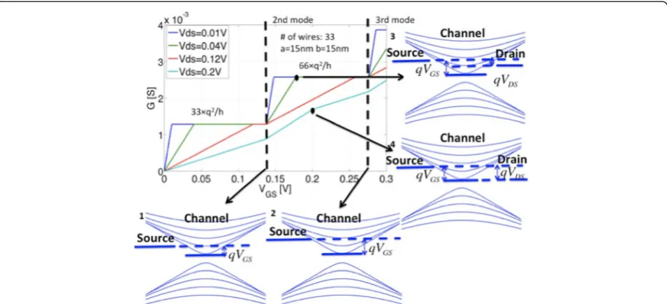
Based on the above analytical framework, I–V character-istics have been calculated for various 1D transport sce-narios. For all simulations, a width of W= 1 μm has been assumed. A set of conductance versus gate voltage curves for different drain voltages is plotted in Fig. 2. For the 1st subband, the conductance saturates at 33⋅ q2/h, where 33 is the total number of wires in the array, with the conductance contribution per wire for one sub-band beingq2/has expected from Eq. 4. The higher the drain voltage, the larger the gate voltage needed to reach the same conductance saturation level.
Fora= 15nm,ΔE=hvf/2a≅0.14 eV, which means that at VGS=m⋅0.14 V the (m + 1)th subband will start to conduct. This situation corresponds to band diagrams 1 and 2 that illustrate the second, third subband at gate voltages of 0.14 and 0.28 V aligned with the source Fermi level. For VDS= 40 mV,VGS= 0.18 V (diagram 3) maximum conductance through two subbands occurs since the minimum of the second subband is exactly by the amount of VDSbelow the source Fermi level. Thus, even a further increase of gate voltage does not change the conductance until the third mode starts to conduct.
Only when VGS=VDS+m⋅0.14 V, the conductance
through the (m + 1)th mode will saturate. Accordingly, for VDS= 200 mV,VGS= 200 mV (diagram 4), only the first mode in each wire has reached its saturation
conductance ofq2/hwhile the second mode has not. For gate voltage values below 200 mV, an increase in gate voltage leads to more conduction in both, the first and second mode. However, for gate voltages above 200 mV, an increase in gate voltage only leads to more conduction
in the second mode. As a result, the slope of conductance versus gate voltage decreases at this point.
[image:4.595.60.538.89.307.2]Next, we compare the current levels in 1D and 2D. In Fig. 3a, both, the 1D current (blue) and the 2D current (red) are plotted as a function of gate voltage. It is clear
Fig. 2Calculated conductance versus gate voltage for different drain voltages. The diagrams indicate the relative position of the 1D subbands for the respective drain and gate voltage conditions. Diagrams 1 and 2 show the band alignment when the second, third mode starts to conduct. Diagram 3 shows the band alignment for current saturation. Diagram 4 shows the band alignment when only the first mode is saturated but not the second mode
Fig. 3aIDversus VGSfor both, the 1D and 2D case.b3D plot of I1D–I2D(z-axis: I1D–I2D,x-axis: VGS,y-axis: VDS), theblack lineindicates where the
1D current and the 2D current are equal.c2D projection ofb. d3D plot for gm1D–gm2D(z-axis: gm1D–gm2D,x-axis: VGS,y-axis: VDS), theblack line
[image:4.595.58.539.447.694.2]that for small gate voltages, the 1D current can exceed the 2D counterpart as mentioned above in the context of Eq. 4. The crossing points are labeled from small drain voltages to large drain voltages as: 1, 2, 3, and 4. The corre-sponding positions are shown in Fig. 3c, and it is obvious that for drain voltages larger thanVDS=ΔE/q= 0.14 V, the position of the crossing point occurs at the same gate volt-age of VGS=ΔE/q= 0.14 V. For drain voltages below 0.14 V, the crossing points depend linearly on gate voltage, andVGSapproachesΔE/2q= 0.07 V when the drain voltage tends to zero. Note that, as stated earlier, the assumption of operation in the QCL for both the 1D and 2D case is a conservative estimate that it will overestimate the band movement in the 2D case resulting in an underestimated gate voltage range for which 1D exhibits a larger current than 2D. In terms of transconductance gm, 1D can also exceed the 2D case for certain bias conditions (shown in Fig. 3d). Interestingly, this statement even holds true for largeVGSvalues as long asVDSis small enough because of the onset of higher 1D modes.
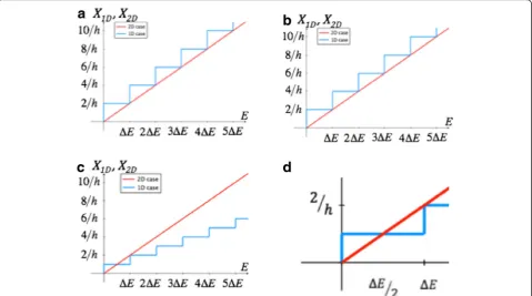
Next, we will illustrate based on the DOS of 1D versus 2D how 1D currents can exceed their 2D counterparts. As discussed before, both 1D and 2D currents can be expressed as an energy integral of the number of conduct-ing modes M1D, 2D(E) and the difference of the source and drain Fermi distributions. If we compare M1Dfor a wire of widthawith its counterpart in 2D:aM2D, one can derive the following expressions:
X2D ¼aM2D¼
2Ea
hvf ð5Þ
X1D ¼M1D¼ int
2Ea
hvf
ð6Þ
Equation 5 was multiplied by the wire width a for a proper comparison of the 2D and 1D number of modes. Obviously, Eq. 6 is just the discrete version of Eq. 5 as shown in Fig. 4. Depending on the choice of threshold voltage (ΔEin case of Fig. 4a and zero in case of Fig. 4b), X1D is smaller or larger than X2D. From Fig. 4b, one might conclude that the 1D case is always providing lar-ger currents, but in reality, the material loss that is cap-tured by the above-introduced parameter b needs to be considered as well. If we choose a=b, the material loss results in a scenario as depicted in Fig. 4c. Under these conditions, X1D is larger than X2D only for VGS<ΔE/q. The exact conditions under which the 1D current can be larger than the 2D counterpart can be calculated by comparing ∫X1DdE and ∫X2DdE. As shown in Fig. 4c, d, X1Dis only larger for the energy region from 0 toΔE/2, and for the integration range (0,ΔE), ∫X1DdE and ∫X2DdE are identical. This means that for VGS larger than ΔE/q= 0.14V, the 2D current will be always larger which confirms the results in Fig. 3c. Equation 7 sum-marizes the conditions under which the 1D current ex-ceeds the 2D one:
Fig. 4aX1DandX2D,respectively, as defined in the text,bsituation as inaafter threshold voltage shift,csituation as inaafter threshold voltage
shift and accounting for material loss, anddzoom ofc
[image:5.595.59.539.434.701.2]qVGS< Δ
EþqVDS
ð Þ
2 qVDS≤ΔE
qVGS<ΔE qVDS >ΔE
8 <
: ð7Þ
Note that Eq. 7 describes exactly the black line in Fig. 3c. If scattering is considered as discussed above, a scaling parameter that captures excess scattering in the ribbon case will have to be introduced in Eq. 7, which will reduce the voltage range over which the 1D currents are larger than the 2D ones.
In the following, we want to focus on the interplay
between a and b. As discussed above, the 1D current
depends on both parameters, and depending on the
in-troduced quantization conditions through a and the
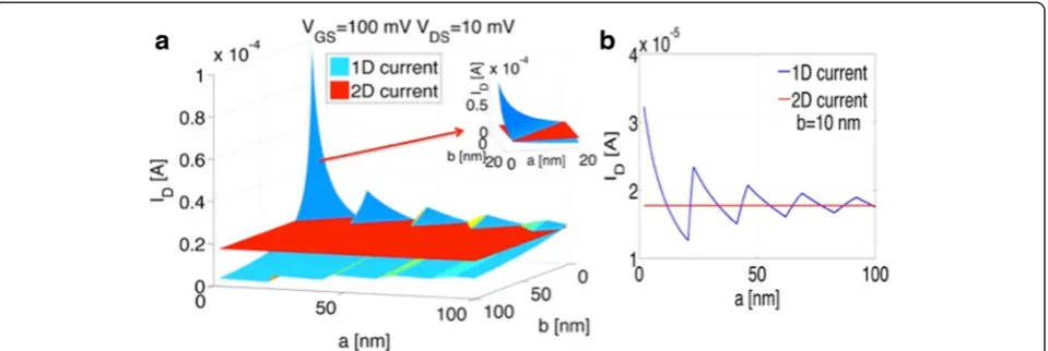
material loss throughb,I1D will exceed (or not)I2D. To illustrate this point, both the 1D and the 2D currents are plotted for different a,b-values in Fig. 5 for a linear and in Fig. 6 for a parabolic energy dispersion.
Since in general, different E(k) dispersion relations impact the above analysis only in so far that the density of states and energy quantization ΔE is changed, both, Figs. 5 and 6 show qualitatively the same dependences. While the energy dispersion impacts the values of the
parametersa, b,VDS, andVGS for which the 1D current can exceed the 2D counterpart, the general trends de-scribed above prevail. In particular, Eqs. 1, 3, and 4 are valid independent of the exact material choice. For the details of how Eq. 2 and the number of 1D modesm(E) are modified under the assumption of a parabolic energy dispersion, see the appendix.
For (a,b) = (0,0),I1Dbecomes infinite since the number of wiresW/(a + b) contributing q2/hto the conductance becomes infinite. Also, as expected, smallb-values are in general desirable to reduce the amount of material loss. Thea-dependence is somewhat more surprising. In fact, we find a non-monotonic dependence of the 1D current with a for constant b as shown in Fig. 5b. Two effects need to be considered when a increases. On one hand, the number of contributing wires decreases with increas-ingafor fixedWandb. This results in aI1D∝1/atrend as depicted in Fig. 5b. On the other hand, increasing a changes the quantization conditions per wire and de-creases the mode spacing ΔE. The sharp increases in current around 21, 42, and 63 nm are a result of this effect. For these a-values, ΔE is 100, 50, and 25 meV, respectively. From the discussion above, the number of
Fig. 51D current and 2D currents are plotted as a function ofaandbfor a linear E(k)-relation
[image:6.595.60.540.89.250.2] [image:6.595.61.540.574.715.2]contributing modes at source Fermi level is simply int(qVGS/ΔE+ 1) which implies that for a= 21, 42, and 63 nm, the second, third, and fourth mode starts
con-ducting for a VGS of 100 mV. The amount of current
change at the onset of the nth mode is proportional to n/(n−1) which implies a current increase by a factor of 2, 1.5, and 1.33 at a= 21, 42, and 63 nm, respectively, consistent with Fig. 5b.
Off-State Performance
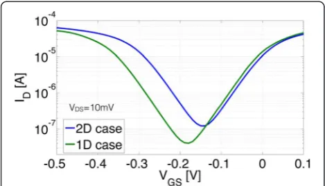
So far, the discussion had only been concerned with the on-state performance of an array of 1D wires in com-parison with their 2D counterpart. In this section, we will discuss that the abovementioned benefits of a higher on-current in 1D for certain parameters do in fact not come at the expense of a deteriorated off-state perform-ance of the device. In order to come to this conclusion, currents through both, the conduction and valence band need to be considered. If a band gap is assumed in a semiconductor with parabolic bands (see also Fig. 6), size quantization increases the energetic spacing between the maximum of the valence band and the minimum of the conduction band for the 1D case. To quantify the impact of this band gap change, the above condition about zero Kelvin operation needs to be revised since, otherwise, an infinitely steep inverse subthreshold slope and, accord-ingly, an infinite on/off-current ratio would make the comparison between the 2D and 1D scenario meaningless. Figure 7 shows transfer characteristics for both, the 1D and the 2D case at 300 K. As apparent from the plot, the quantization conditions in the nanowires result in a larger band gap that leads to a larger on/off-current ratio, i.e., in particular, a substantially lower minimum current level as shown in Fig. 7.
Conclusions
In conclusion, we have presented in this article a simple analysis focusing on both the on-current in arrays of
one-dimensional wires if compared to a two-one-dimensional struc-ture of similar dimensions. Different from general expecta-tions, an array of 1D structures can outperform the current in a 2D system if threshold voltages are properly adjusted, even under room temperature operation. The above discus-sion provides a simple guide to perform similar compari-sons for other material systems and device structures.
Additional file
Additional file 1:On the Current Drive Capability of Low Dimensional Semiconductors -1D versus 2D–. The current calculation for parabolic E-k relation and the disscusion of temperture de-pendence is shown in the addtional file.Figure S1.shows the difference of 1D and 2D currrent under T=0k & T=300K.
Competing Interests
The authors declare that they have no competing interests.
Authors’Contributions
JA led the effort. YZ carried out the calculation. Both author discussed the result and commented on the manuscript. All authors read and approved the final manuscript.
Acknowledgement
Research support for YZ and JA was provided in part by a Field Work Proposal, sponsored by the US Department of Energy, Basic Energy Sciences, and Materials Sciences and Engineering Division located at Brookhaven National Laboratory, which is supported by the US Department of Energy under contract no. DE-AC02-98CH10886.
Received: 15 July 2015 Accepted: 19 October 2015
References
1. Hisamoto D, Lee WC, Kedzierski J, Takeuchi H, Asano K, Kuo C, Anderson E, King TJ, Bokor J, Hu C. (2000) FinFET—a self-aligned double-gate MOSFET scalable to 20 nm. IEEE Trans Electron Devices 47:2320–2325.
2. Huang XJ, Lee WC, Kuo C, Hisamoto D, Chang LL, Kedzierski J, Anderson E, Takeuchi H, Choi YK, Asano K, Subramanian V, King TJ, Bokor J, Hu C. (2001) Sub-50 nm p-channel FinFET. IEEE Trans Electron Devices 48:880–886. 3. Kedzierski J, Ieong M, Nowak E, Kanarsky TS, Zhang Y, Roy R, Boyd D, Fried
D, Wong HSP. (2003) Extension and source/drain design for high-performance FinFET devices. IEEE Trans Electron Devices 50:952–958. 4. Kedzierski J, Nowak E, Kanarsky T, Zhang Y, Boyd D, Carruthers R, Cabral C,
Amos R, Lavoie C, Roy R, Newbury J, Sullivan E, Benedict J, Saunders P, Wong K, Canaperi D, Krishnan M, Lee KL, Rainey BA, Fried D, Cottrell P, Wong HSP, Ieong M, Haensch W. Metal-gate FinFET and fully-depleted SOI devices using total gate silicidation. IEDM. 2002;247–250. doi:10.1109/ IEDM.2002.1175824.
5. Lansbergen GP, Rahman R, Wellard CJ, Woo I, Caro J, Collaert N, Biesemans, Klimeck G, Hollenberg LCL, Rogge S. (2008) Gate-induced quantum-confinement transition of a single dopant atom in a silicon FinFET. Nature Phys 4:656–661.
6. Pei G, Kedzierski J, Oldiges P, Ieong M, Kan ECC (2002) FinFET design considerations based on 3-D simulation and analytical modeling. IEEE Trans Electron Devices 49:1411–1419
7. Giannetta RW, Olheiser TA, Hannan M, Adesida I, Melloch MR (2005) Conductance quantization and zero bias peak in a gated quantum wire. Phys E 27:270–277
8. Javey A, Guo J, Wang Q, Lundstrom M, Dai HJ (2003) Ballistic carbon nanotube field-effect transistors. Nature 424:654–657
9. Franklin AD, Chen Z (2010) Length scaling of carbon nanotube transistors. Nature Nanotech 5:858–862
10. Frank DJ, Dennard RH, Nowak E, Solomon PM, Taur Y, Wong HSP (2001) Device scaling limits of Si MOSFETs and their application dependencies. Proc IEEE 89:259–288
Fig. 7Transfer characteristics for the 1D and 2D case for a parabolic E(k)-relation. As above, a width ofW= 1μm anda= 10 nm,b= 4 nm has been assumed
[image:7.595.56.291.89.223.2]11. Guo J, Datta S, Lundstrom M (2004) A numerical study of scaling issues for Schottky-barrier carbon nanotube transistors. IEEE Trans Electron Devices 51:172–177
12. Shin M, Lee J, Ahn C (2008) Simulation study of the scaling behavior of top-gated carbon nanotube field effect transistors. J Nanosci Nanotech 8:5389–5392 13. Meric I, Dean CR, Young AF, Baklitskaya N, Tremblay NJ, Nuckolls C, Kim P,
Shepard KL. (2001) Channel length scaling in graphene field-effect transistors studied with pulsed current–voltage measurements. Nano Lett 11(3):1093–1097.
14. Chen ZH, Appenzeller J. Mobility extraction and quantum capacitance impact in high performance graphene field-effect transistor devices. IEDM. 2008;509–512. doi:10.1109/IEDM.2008.4796737
15. Luryi S (1988) Quantum capacitance devices. Appl Phys Lett 52:501–503 16. Gunlycke D, White CT (2008) Tight-binding energy dispersion of
armchair-edge graphene nanostrips. Phys Rev B 77:115–116
17. Brey L, Fertig HA (2006) Electronic states of graphene nanoribbons studied with Dirac equation. Physical Rev B 73:235411
18. Baringhaus J, Ruan M, Elder F, Tejeda A, Sicot M, Ibrahimi AT, Li AP, Jiang Z, Conrad EH, Berger C, Tegenkamp C, Heer DWA. (2014) Exceptional ballistic transport in epitaxial graphene nanoribbons. Nat 505:349–356.
19. Fang T, Konar A, Xing HL, Jena D (2008) Mobility in semiconducting graphene nanoribbons: phonon, impurity, and edge roughness scattering. Physical Rev B 78:205403
20. Shin YS, Son YJ, Jo MH, Shin YH, Jang HM (2011) High-mobility graphene nanoribbons prepared using polystyrene dip-pen nanolithography. J Am Chem Soc 133:5623–5625
Submit your manuscript to a
journal and benefi t from:
7Convenient online submission 7Rigorous peer review
7Immediate publication on acceptance 7Open access: articles freely available online 7High visibility within the fi eld
7Retaining the copyright to your article