N A N O E X P R E S S
Open Access
Electromagnetic modeling of waveguide amplifier
based on Nd
3+
Si-rich SiO
2
layers by means of
the ADE-FDTD method
Christian Dufour
*, Julien Cardin, Olivier Debieu, Alexandre Fafin and Fabrice Gourbilleau
Abstract
By means of ADE-FDTD method, this paper investigates the electromagnetic modelling of a rib-loaded waveguide composed of a Nd3+doped Silicon Rich Silicon Oxide active layer sandwiched between a SiO2bottom cladding and a SiO2 rib. The Auxilliary Differential Equations are the rate equations which govern the levels populations. The Finite Difference Time Domain (FDTD) scheme is used to solve the space and time dependent Maxwell equations which describe the electromagnetic field in a copropagating scheme of both pumping (lpump= 488 nm) and signal (lsignal= 1064 nm) waves. Such systems are characterized by extremely different specific times such as the period of electromagnetic field ~ 10-15s and the lifetimes of the electronic levels between ~ 10-10s and ~ 10-4s. The time scaling method is used in addition to specific initial conditions in order to decrease the computational time. We show maps of the Poynting vector along the propagation direction as a function of the silicon nanograin (Si-ng) concentrations. A threshold value of 1024Si-ng m-3is extracted below which the pump wave can
propagate so that a signal amplication is possible.
Keywords:Silicon nanograin, Silica, Neodymium, ADE-FDTD, Waveguide, amplification
Introduction
The feasibility of optical amplifying waveguide has been for almost two decades the purpose of numerous experi-mental works [1]. The devices under study were based on an active layer constituted of a silica film co-doped with silicon nanograins (Si-ng) and rare earth ions RE (Er3+in particular) deposited on a substrate and covered by a cladding layer of pure silica. The differences in the opti-cal indices of the three layers ensure the optiopti-cal guiding. The amplification of a signal is based on an efficient population inversion of the rare earth levels whose energy difference correspond to the signal wavelength. Due to the very low RE signal absorption cross section, a solution has been found using silicon nanoparticles. The physical background lies on two major phenomena: on the one hand, the ability of Si-ng’s to absorb efficiently a pumping light and, on the other hand, the effective energy transfer between Si-ng’s and RE ions. In this way, a RE population inversion could have been achieved in
order to fulfill the amplification function of the device. Despite all these promising features, a net gain is hardly achievable with the former Er3+ions due to their great probability of signal reabsorption from the ground state. This drawback is prevented with the use of Nd3+ions described by a five level scheme since the transition does not involve the ground state. The theoretical studies of the waveguide amplifiers have accounted for both rate population equations and Maxwell equations. In this paper we investigate the ADE-FDTD method applied to a rib-loaded waveguide whose active layer is composed of a silica film co doped with Nd3+ ions and silicon nano-grains. One of the main issues to be addressed in such systems consists in dealing with extremely different time scales: the populations lifetimes (1 ms) and the electro-magnetic field period (10-15s). According to [2,3] we use a time scaling that allows to circumvent this issue. All the lifetimes have been shortened by a factor of 106, and consequently the transfer coefficient K has also been divided by the same coefficient. In this paper, we investi-gate the accuracy of this scaling method through longitu-dinal and trans-verse maps of the Poynting vector for
* Correspondence: [email protected]
CIMAP, CEA/CNRS/ENSICAEN/UCBN, 6 Boulevard Maréchal Juin, 14050 Caen Cedex 4, France
several Si-ng concentrations. The applicability of this method is linked to the space and time calculation steps since a reasonable computing time must not be exceeded.
Computational details
We treat the problem within a calculation box as described in Figure 1. Each axis (x,y and z) is divided into space steps (Δx,ΔyandΔzrespectively).
Four zones appear and will be described hereafter: i) the rib-loaded waveguide composed of the active layer (optical index nact = 1.52) stacked between the SiO2 cladding and rib (optical index nsiO2=1.45), ii) the
plane containing the electromagnetic field source (zsource
= 6 Δz), iii) the diaphragm (between 7Δz and 10Δz) which transforms the source into a realistic electromag-netic Gaussian field impinging on the waveguide andiv) the boundary zone (PML) (4Δzin thickness) character-ized by appropriate values of electrical (r) and magnetic (s) conductivities in order to absorb the electromagnetic field so that the box borders do not influence the field in the zone of interest [4].
Lorentz Model for the dielectric susceptibility
Considering a transition between levelsiandjwe use the Lorentz following relationship which makes the coupling between the polarization densityPi j, the level
popula-tionsNiandNjinm-3and the total electric fieldE:
d2P
ij(t)
dt2 +ωij
dPij(t)
dt +ω
2
ijPij(t) =κNij(t)E(t) (1)
Δωijis the FWHM of the ijtransition deduced from
photoluminescence measurements according to [5],
ωij=
2πc
λij is the oscillator pulsation linked to theij
tran-sition wavelengh lij, κ =
6πε0c3γij
ω2
ij
and gij is the ij
radiative transition rate in s-1 [6,7]. The level popula-tions difference in m-3is given byΔNij=Ni-Nj.
In the same way, we describe the polarisation density Psi linked to the silicon level populationsNSi (ground
level) and NSi∗ (excited level),to the oscillator pulsation ωSi and finally to the transition FWHMΔωSi.
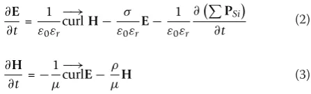
Maxwell equations: FDTD numerical method
We start from the Maxwell equation which links the displacement vectorDto the magnetic excitationH:
∂D ∂t =
−→
curlH−Je
where the current densityJeis related to EbyJe=sE
where s is the electrical conductivity. Accounting for the relationship between D and the total polarisation density,D=ε0E + ∑Pijwe may write:
∂E ∂t =
1
ε0εr
−→
curlH− σ ε0εr
E− 1
ε0εr
∂PSi
∂t (2)
∂H
∂t =−
1
μ −→
curlE− ρ
μH (3)
All the calculations are performed with real variables. Hence, in order to account for absorption processes other than those due to the level transitions, we charac-terize (especially for the diaphragm and PML) a specific electric conductivitysand magnetic conductivityr.
Both equations 2 and 3 are solved using the Yee algo-rithm [8]. The space steps are chosen so that:Δx =Δy = Δz ≪ lmin (the lowest values among all the
wave-lengths) Hereafter: Δx =Δy =Δz = 45 nm. The time
stepΔtmust fulfill the condition:t z
c . Finally the fields inputs (pump and signal) are known as the‘source issue’. Since no perfect source is available, we choose an
xyplane atzsource= 6Δzin which we define a polarized
electric field.Esource= Ex
x,y−→i. This source impinges on the diaphragm so that a Gaussian beam enters the waveguide itself atz=11Δz. The total waveguide length is 15Δz= 0.665μm and the number of time steps is 25000, which amounts to a total simulated time of 0.3 10-12s.
Rate equations
In this section, we detail the ADE part of the method which describes the time population dynamics of Si-ng and Nd3+ levels with the following rate equations. Silicon nanoclusters
We consider both radiative rand non radiativenr tran-sitions. The optical pumping power (in m-3) writes
1
¯
hωp
E(t)dPp(t)
[image:2.595.315.539.304.372.2]RE ions is described by a transfer coefficient K and equal toKN∗Si(t)N0(t)at time t. This leads to the
fol-lowing rate equations:
dNSi∗(t) dt = +
1 ¯ hωp
E(t)dPp(t) dt −
N∗Si(t)
τ∗|r nr
−KN∗Si(t)N0(t), (4)
dNSi(t) dt =−
1 ¯ hωp
E(t)dPp(t) dt +
N∗Si(t) τ∗|r
nr
+KNSi∗(t)N0(t). (5)
Rare earth ions Nd3+
A five level scheme is adopted for the Nd3+ ion in Figure 2 [9,10].
We consider three radiative transitions (4F3/2 ®4I9/2, l20 = 945 nm; 4F3/2 ®4I11/2, l21 = 1064 nm; and 4F3/2® 4I13/2,l24 = 1340 nm) and three non radiative transitions (4F5/2- > 4F3/2 (N3 ↦ N2 ) 4I11/2 - > 4I9/2 (N1 ↦N0) and 4I13/2 - > 4I11/2(N4 ↦N1)).
The terms +¯1 hω21
E(t)dP21(t) dt , +
1
¯
hω20
E(t)dP20(t) dt and
+ 1
¯
hω24
E(t)dP24(t)
dt correspond to the stimulated
transi-tions 2 ® 1, 2 ® 0 and 2 ® 4. The terms−N2(t)
τ21|rnr ,
−N2(t) τ20|rnr
and −N2(t)
τ24|rnr
correspond to the spontaneous
transitions 2® 1, 2®0 and 2®4. The associated rate equations read:
dN3(t)
dt =− N3(t) τ32|nr
+KN∗Si(t)N0(t), (6)
dN2(t) dt =
1 ¯
hω24
E(t)dP24(t) dt +
1 ¯
hω21
E(t)dP21(t) dt
+ 1 ¯
hω20
E(t)dP20(t) dt +
N3(t)
τ32|nr −
N2(t)
τ21|rnr
−N2(t)
τ20|rnr
−N2(t)
τ24|rnr
,
(7)
dN4(t)
dt =− 1
¯
hω24
E(t)dP24(t) dt +
N2(t) τ24|rnr
−N4(t) τ41|nr
, (8)
dN1(t) dt =−
1 ¯
hω21
E(t)dP21(t) dt +
N2(t)
τ21|rnr
−N1(t)
τ10|nr
+N4(t)
τ41|nr
, (9)
dN0(t)
dt =− 1
¯
hω20
E(t)dP20(t) dt +
N2(t) τ20|rnr
+N1(t)
τ10|nr
−KN∗Si(t)N0(t).
(10)
Application to rib-loaded waveguide
In table 1, we collect the simulation parameters taken into account for the transitions. The lifetimes corre-spond to the experimental ones divided by the scaling factor 106.
The transfer coefficient K estimated to ~ 10-20m3s-1 [11] has also been scaled with the same factor 106:K= 10-14 m3.s-1. The amplitudes of the input pumping and signal electric fields have been taken equal to Epump =
107V.m-1andEsignal= 100 V.m-1.
After the time Fourier transform of both Eand H fields, we deduce the zcomponent of the pump (Rpumpz )
and signal (Rsignal
z ) Poynting vectors (in W.m.
-2 )
Three Si-ng concentrations have been investigated (Nsi = 1025, 1024and 1023 m-3 ). In the initial states,
only the ground level is populated. The corresponding (xz) maps (Rpumpz ) are plotted in Figures 3, 4 and 5.
[image:3.595.315.540.86.268.2] [image:3.595.54.296.273.699.2]In these figures, the different calculation box zones may be recognized: i) the Perfectly Matched Layer (PML) which lies in the area from the lefthand side between z = 0 nm and z = 180 nm, and from the
[image:3.595.305.540.595.700.2]Figure 2Five level scheme of Nd3+ions.
Table 1 Simulation parameters of the Si-ng and Nd3+ transitions
Transition lifetime(s) type ωij(s-1) Δωij(s-1)
Si®Si * 4 10-11 R 3.86 1015 4.4 1014
3®2 2.3 10-16 NR
2®0 3 10-10 R 2.07 1015 1.38 1014 2®1 3 10-10 R 1.7 1015 1.39 1014 2®4 3 10-10 R 1.3 1015 1.33 1014 4®1 9.7 10-16 NR
1®0 5.1 10-16 NR
righthand side between z = 890 nm and z = 1000 nm,
ii) the plane containing the electromagnetic field source at z ~ 300 nm, iii) the FDTD zone which is located at about 180 nm from border of plot, the Gaussian beam impinging in the waveguide at z ~ 500 nm and the intensity propagating in waveguide from z ~ 500 nm to z ~ 900 nm.
On the basis of the parameters taken from experi-ments, these plots evidence the fact that for Si-ng con-centrations above 1024m-3, the pumping wave does not reach the end of the waveguide. This concentration threshold corresponds to high experimental values [12], and is above the lower values leading to minimal optical losses [1].
In order to reduce the computing time, in addition to the scaling method, we start the calculations with Si-ng levels already populated at the maximum inversion rate, NSi=N∗Si= 5 10
22
m-3. Hence, for a given total Si-ng concentration of 1023 m-3, this result (Figure 6) can be compared to the preceding one where NSi= 1023 m-3
andN∗Si = 0(Figure 5). The propagation of the pump power within the waveguide seems to be similarly atte-nuated in both cases. The main difference occurs in the
N3 level concentration which is directly populated from the excitedN∗Silevel. In case of maximum inversion rate, the stationary regime is reached and the concentration becomes equal toN3=τ32.K.NSi∗.N0≈1.11018 m-3. In
[image:4.595.303.539.85.283.2]case of NSi = 1023 m-3 and N∗Si= 0 starting Figure 3(yz) maps ofRpumpz in W.m-2for [Si-ng] = 1025m-3,
[image:4.595.56.294.87.280.2]the dashed-dot rectangle represents the waveguide rib.
Figure 4(yz) maps ofRpumpz in W.m-2for [Si-ng] = 1024m-3,
[image:4.595.56.293.509.699.2]the dashed-dot rectangle represents the waveguide rib.
Figure 5(yz) maps ofRpumpz in W.m-2for [Si-ng] = 1023m-3,
the dashed-dot rectangle represents the waveguide rib.
Figure 6(yz) map ofRpumpz in W.m-2N
[image:4.595.303.539.509.701.2]concentration, the N3 concentration does not reach a stationary regime and stays below several 1017m-3.
Conclusion
We have investigated by means of ADE-FDTD method the electromagnetic field propagation in rib-loaded waveguides constituted of an active layer of Nd3+doped silicon rich silica stacked between pure silica bottom cladding and rib. This numerical method treats Nd3+ and Si-ng levels rate equations (ADE) coupled to the Maxwell equations (FDTD). The extremely different spe-cific times involved in the ADE (levels lifetimes≈10μs) and in FDTD (electromagnetic wave periods≈10-15s) have required the use of the scaling time method which allows reasonable computing time: the number of time iterations has been reduced by six orders of magnitude. In addition to this method, we have proposed to start the cal-culations with steady state Si-ng ground and excited popu-lations. The numerical computation has been performed for several Si-ng concentrations. Therefore we can infer that the pumping wave propagation (lpump= 488 nm ) is
possible for [Si-ng]≤1024m-3in agreement with experi-mental loss measurements. The upper Nd3+level reaches its stationary value predicted with the analytical solution of the steady state rate equations.
Acknowledgements
The authors are grateful to the French Agence Nationale de la Recherche, which supported this work through the Nanoscience and Nanotechnology program (DAPHNES project ANR-08-NANO-005).
Authors’contributions
CD and JC conceived the calculation code, AF carried out most of the calculations, OD performed the optical measurements on our samples and FG conceived the whole project. All authors read and approved the final manuscript.
Competing interests
The authors declare that they have no competing interests.
Received: 27 September 2010 Accepted: 4 April 2011 Published: 4 April 2011
References
1. Navarro-Urrios D, Melchiorri M, Daldosso N, Pavesi L, García C, Pellegrino P, Garrido B, Pucker G, Gourbilleau F, Rizk R:Optical losses and gain in silicon-rich Silica waveguides containing Er ions.Journal of Luminescence
2006,121:249-255.
2. Shi S, Prather DW:Lasing dynamics of a silicon photonic crystal microcavity.Opt Express2007,15(16):10294-10302.
3. Redding B, Shi S, Creazzo T, Prather DW:Electromagnetic modeling of active silicon nanocrystal waveguides.Opt Express2008,16:8792-8799. 4. Berenger JP:A perfectly matched layer for the absorption of
electromagnetic waves.J of Computational Physics1994,114(2):185-200. 5. Biallo D, De Sario M, Petruzzelli V, Prudenzano F:Time domain analysis of
optical amplification in Er3+ doped SiO2-TiO2 planar waveguide.Opt Express2005,13(12):4683-4692.
6. Taflove A, Hagness SC,et al:Computational electrodynamics: the finite-difference time-domain method.Artech House Norwood, MA1995. 7. Zhukovsky SV, Chigrin DN:Numerical modelling of lasing in
microstructures.Phys Status Solidi (b)2007,244(10):3515-3527.
8. Yee K:Numerical solution of inital boundary value problems involving Maxwell’s equations in isotropic media IEEE Transactions on antennas and propagation.1966,14(3):302-307.
9. Serqueira EO, Dantas NO, Monte AFG, Bell MJV:Judd Ofelt calculation of quantum efficiencies and branching ratios of Nd3+ doped glasses.J of Non-Crystalline Solids2006,352(32-35):3628-3632.
10. Pecoraro E, Sampaio JA, Nunes LAO, Gama S, Baesso ML:Spectroscopic properties of water free Nd2O3-doped low silica calcium aluminosilicate glasses.J of Non-Crystalline Solids2000,277(2-3):73-81.
11. Pacifici Domenico, Franzò Giorgia, Priolo Francesco, Iacona Fabio, Dal Negro Luca:Modeling and perspectives of the Si nanocrystals-Er interaction for optical amplification.Phys Rev B2003,67(24):245301. 12. Gourbilleau F, Levalois M, Dufour C, Vicens J, Rizk R:Optimized conditions
for an enhanced coupling rate between Er ions and Si nanoclusters for an improved 1.54-μm emission.J Appl Phys2004,95:3717.
doi:10.1186/1556-276X-6-278
Cite this article as:Dufouret al.:Electromagnetic modeling of waveguide amplifier based on Nd3+Si-rich SiO2layers by means of the
ADE-FDTD method.Nanoscale Research Letters20116:278.
Submit your manuscript to a
journal and benefi t from:
7Convenient online submission
7 Rigorous peer review
7Immediate publication on acceptance
7 Open access: articles freely available online
7High visibility within the fi eld
7 Retaining the copyright to your article

![Figure 5 (yz) maps of Rpumpzin W.m-2 for [Si-ng] = 1023 m-3,the dashed-dot rectangle represents the waveguide rib.](https://thumb-us.123doks.com/thumbv2/123dok_us/8848383.933977/4.595.56.293.509.699/figure-maps-rpumpzin-si-dashed-rectangle-represents-waveguide.webp)
